Daanish M. Khan
Digital Voltmeter Using Atmel AVR AT90S CPU
And Maxim 1110 ADC
This is a very simple design for a digital Voltmeter using an Atmel AVR AT90S1200 RISC CPU development board and a MAXIM 1110 ADC.
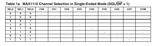
The MAXIM 1110 is a multichannel ADC capable of unipolar or bipolar conversion with an internal reference of +2.048 V. It receives an 8 bit command byte based on which it performs a conversion. The details of the byte are given in Table 1. The conversion can use either an external clock clocked through SCLK or the internal clock.
Table 1. Command Byte Format
|
Bit 7 (MSB) |
Bit 6 |
Bit 5 |
Bit 4 |
Bit 3 |
Bit 2 |
Bit 1 |
Bit 0 (LSB) |
|
Start |
Sel 2 |
Sel 1 |
Sel 0 |
Uni/Bip |
Sgl/Dif |
PD1 |
PD0 |
|
Bit |
Name |
Description |
|
7 |
Start |
The first logic "1" after CS goes low defines the beginning of the control byte |
|
6 5 4 |
Sel 2 Sel 1 Sel 0 |
Select which of the input channels are to be used for conversion (Table 1a) |
|
3 |
Uni/Bip |
1=unipolar, 0=bipolar, selects unipolar or bipolar conversion mode. Select differential operation for bipolar mode |
|
2 |
Sgl/Dif |
1=single ended, 0= differential mode, selects single ended or differential conversions. In single ended, input signal voltages are referred to COM.In differential mode, voltage difference between two channels is measured |
|
1 |
PD1 |
1=fully operational, 0=power down. Selects fully operational or powerdown |
|
0 |
PD0 |
1=external clock, 0=internal clock. Selects between internal clock and external clock mode/ |
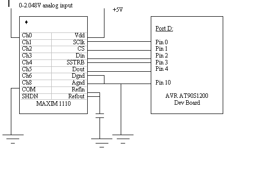
Figure 1 shows the design of the circuit, along with pin connections between the ADC and the development board. Also make sure that PORTB is connected to the LED pins for output.
We start by clearing the CS bit so the select the ADC. The command byte is then clocked in, for a Unipolar single ended conversion on channel 0. While a conversion is being performed, SSTRB is low. Once conversion is complete SSTRB goes to high and we can start reading in the serial output from the ADC. Note here that the first 2 bits of the output are zeros and need to be discarded. The next 8 bits give the value of the input as a fraction of the Reference. These bits are read into a register using the carry flag and rotating it through the register based on whether the input bit is high or low (see code section ADC_RECEIVEDATA).
To interpret the output byte suppose your LED’s give a value of D7 (light on implies a 1 and with the leftmost bit as the MSB) the value of the input is (216(D7)*Vref)/256. (For a detailed description see the datasheet for the ADC pp 17-18 http://www.maxim-ic.com/efp/ADconv.htm ). So in our case a byte D7 would correspond to (216*2.048)/256 shich is 1.728V.
The CPU checks and displays the value continuously until it is turned off or the reset button is pressed.
Figure 1. Schematics of the circuit
;***************************************************************************
 ;* DVM.ASM
 ;*
 ;*Simple program that uses a MAXIM ADC and communicates to it sending commands for
 ;*conversion and receiving a byte of output from the ADC
 ;**************************************************************************
 .DEVICE AT90S1200

 ;* Two useful macros
 .LISTMAC

 ;skip next instruction if carry set
 .MACRO skipcs
     .SET    _skipcs = PC+2
     brcs    _skipcs
 .ENDMACRO

 ;skip next instruction if carry clear
 .MACRO skipcc
     .SET    _skipcc = PC+2
     brcc    _skipcc
 .ENDMACRO

 ;***************************************************************************

 ;include AT90S1200 registers definitions
 .include "1200def.inc"

 .CSEG
     ;temp variables to be used in the program
     .def    Arg1 =  r20

     ;Variables used to store bytes that are to be sent to and received from ADC
     .def    Main1 = r24     ;contains the cammand byte
     .def    Main2 = r25     ;general purpose counter
     .def    Main3 = r26     ;the incoming byte

 ;***************************************************************************
 ;* Port Pin Assignements
 ;***************************************************************************

     ;port D bit definitions, outputs to ADC and input from it
     .equ    ADCSCLK =     0    ;ADC serial clock output
     .equ    ADCCS =       1    ;ADC chip select (active low)
     .equ    ADCDIN =      2    ;ADC serial data
     .equ    ADCDout =     3    ;ADC output
     .equ    ADCSTRB =     4    ;ADC STROBE output to signal end of conversion
     ;* port B is all outputs to the led's

 ;***************************************************************************
 ;*
 ;* MAIN PROGRAM
 ;*
 ;***************************************************************************
 ;* INITAILIZATION
 ;***************************************************************************

 RESET:
     ldi    Arg1, 0b000011100 ;set bits 2,3,4 to outputs and all
     out    ddrd, Arg1        ;others to inputs. Pin 4 reads the
                              ;the ADC output
     clr    Arg1              ;set SCLK, CS and DIN to zeros
     out    portd, Arg1
     ser    Arg1              ;set port B to outputs
     out    ddrb, Arg1
     out    portb, Arg1       ;turn off LEDs

 ;****************************************************************************
 ;*  READADC: reads ADC channel specified by Main1 into Main3-4
 ;*  Range is 0-4096. Uses Main2
 ;****************************************************************************

 .MACRO  ADC_CLOCKPULSE
 ;makes a clock pulse: ADC reads and outputs data on
 ;falling edge of the clock
     sbi     PortD, ADCSCLK              ;SCLK high
     .SET    _nextstep = PC+1            ;wait at least 200 nS
     rjmp    _nextstep
     .SET    _nextstep = PC+1
     rjmp    _nextstep
     cbi     PortD, ADCSCLK              ;SCLK low
 .ENDMACRO

 READADC:

     cbi    portD, ADCSCLK     ;clear the clock line
     cbi    portD, ADCCS       ;chip select the ADC
     ldi    Main1, 0b10001110  ;the ADC command word
                     ;unipolar (channel1) single ended conversion
                     ;with internal clocking
                     ;Change this for different functions of the
                     ;ADC such as bipolar conversion or external
                     ;clocking.

     ldi    Main2,8  ;the bit counter

 ADC_SENDCOMMAND:
     rol    Main1            ;shift out the 8-bit command
     skipcc
     sbi    portD,ADCDin     ;set the bit in Din
     skipcs
     cbi    portD, ADCDin    ;clear the bit in Din
     ADC_CLOCKPULSE          ;clock the value in
     dec     Main2
     brne    ADC_SENDCOMMAND

     ;ldi    Main2,100

 _WAITLOOP:
     sbic    portD, ADCSTRB    ; wait until you receive a signal from strobe
     rjmp    _WAITLOOP
     clr     Main3              ;refresh Main 3
     ldi     Main2, 10          ;shift in 8+2 bit result (2 leading 0's)

 ADC_RECEIVEDATA:
     clc                ;first set the carry
     ADC_CLOCKPULSE     ;clock the ADC for next bit
     sbis    PinD, ADCDOUT  ;if ADC data low is high, set carry
     sec                    ;inverted since low turns led on
     rol     Main3          ;shift carry into data buffer
     dec     Main2
     brne    ADC_RECEIVEDATA;repeat until all bits read
     sbi     PortD, ADCCS   ;release ADC chip select

 END:
     out     portb, Main3        ;output result to LED’s

 EVER:
    rjmp     READADC        ;Go for another conversion