Junpeng Wang, jw2299
Kevin Pu, kp394
For this project, we constructed an oscilloscope using the PIC32. The inspiration for this project came from the oscilloscopes we used in lab throughout the semester. These oscilloscopes allowed people to view and understand the behavior of a circuit. Without oscilloscopes, many of the circuits we built in class would have been extremely difficult to build. Our goal was to create our own oscilloscope that could accurately read voltages and display the voltage waveforms on a closed circuit TV.
We designed a cheap, portable, yet powerful oscilloscope that is useful in signal verification within embedded systems development. The oscilloscope has 10-bit-resolution accurate reading of analog voltage for voltage signal below 100 KHz frequency. It is able to change its display setting under user command to adapt to signals of different frequency (from 0 up to 100kHz) and amplitude (from 0 up to 3.3V). It also have configurable ground level and trigger level. It uses NTSC TV as video output at 30 frames per second.
While doing design project on embedded systems, we found out that usually we are tied to the laboratory simply because we need some basic functions from an oscilloscope. Therefore, we intend to design a cheap, portable, yet powerful oscilloscope that is useful in signal verification within embedded systems development. The oscilloscope should have accurate reading of analog voltage for high-frequency voltage signal.The oscilloscope should be able to change its display setting under user command to adapt to signals of different frequency and amplitude.
Voltage Signal input goes into the internal ADC of PIC32. Stimulated by the internal Timer of PIC32, the ADC samples 256 samples of the voltage signal at a frequency specified by user, and send the array to data RAM via Direct Memory Access.
The array is then mapped to a screen buffer, which represent the bitmap of the television screen. The bitmap is also masked with grids for measurements, arrows to show ground and trigger level, and a title string showing the current user configuration on the top. The screen buffer is sent to the television in NTSC protocol simulated by the SPI bus and Output Comparators internal to PIC32.
There are four devices for user inputs. Two potentiometers that allows change in ground level position on screen and trigger level. Two rotary encoders that allows change in time-per-division and voltage-per-division representations of the grids shown on screen.
The video output signal follows NTSC standard and is compatible with any NTSC TV. Since most TV in the United States are NTSC-compatible, our oscilloscope can used most TV found in the United State as output in an 256X200 pixel area. There is no patents, copyrights, or trademark considerations relevant to this project.
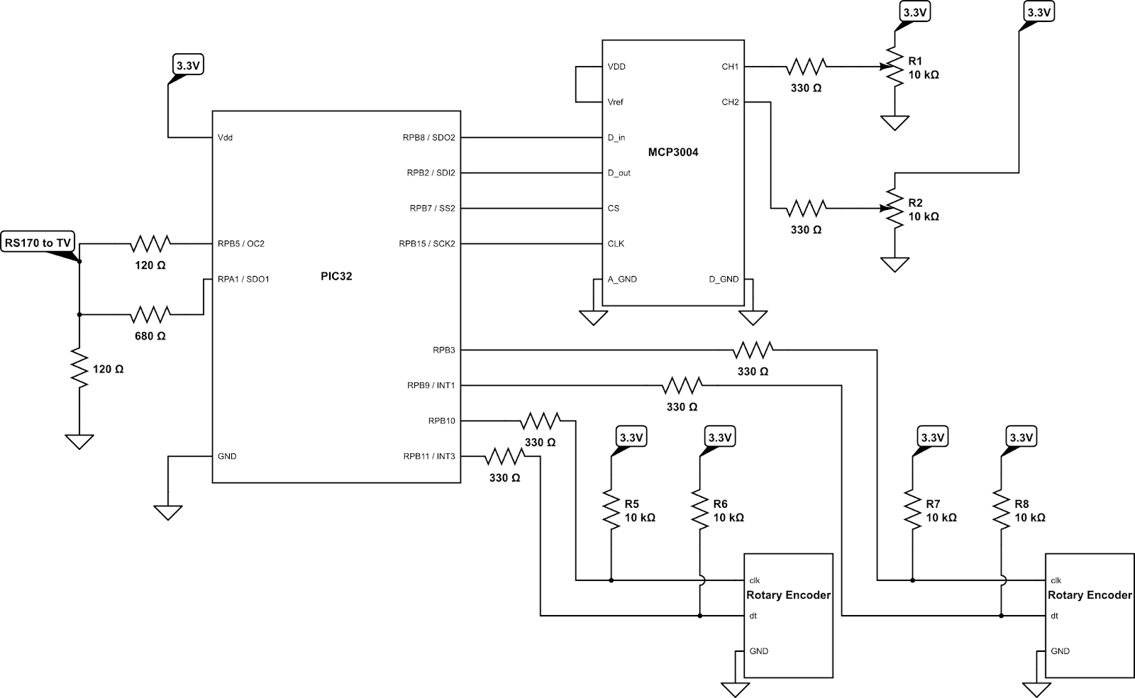
Figure 1. Overall System Schematics
A PIC32 microcontroller (model pic32mx250f128b, datasheet available at: http://www.microchip.com/wwwproducts/en/PIC32MX250F128B) is responsible for sampling mixed-signal input, synthesizing NTSC signal, and taking in user inputs.
The internal ADC of the PIC32 has a maximum conversion speed of 1Msps and a resolution up to 10-bits, which are fast and accurate enough to read voltage signal up to 100kHz. The ADC also have a selectable conversion trigger source, which we tie to Timer3 interrupt within PIC32 to control the sampling frequency of the ADC, in real time under user command.
The PIC32 has Direct Memory Access, which we use to move the large array of ADC samples to data RAM, and move the 6400-byte-long screen buffer to SPI bus. This feature is necessary for us to meet the strict time constraint generating NTSC signal and updating the screen at 30 frame per second.
The SPI module of the PIC32 has two channels. We use channel 1 for NTSC signal generation, and channel 2 for interfacing with MCP3004 to expand the number of analog inputs. The very customizable nature of the SPI in PIC32 allows using the SPI signal to simulate NTSC signal, as well as following a certain interface protocol with MCP3004.
We rely on the external interrupt capability of PIC32 to read the rotary encoders accurately without affecting the overall performance of the system.
We need PIC32 to read analog voltage level from two potentiometers to adjust oscilloscope Y-axis position and trigger level, yet we have already assigned the internal ADC of PIC32 to reading the high-frequency voltage signal input. Therefore, we use an external ADC MCP3004 (datasheet available at: http://www.microchip.com/wwwproducts/en/MCP3004).
Figure 2. MCP3004 Schematics
MCP3004 has 4 channels of analog input. For our project we only use CH1 and CH2. Each linear 10Kohm potentiometer (we use https://www.sparkfun.com/products/9288) has terminal 1 and 3 connected to Vdd of 3.3V and ground, and has its terminal 2 connected to one channel input of MCP3004. Each channel has a protective 330ohm resistor to prevent short to Vdd. The analog ground and digital ground of MCP3004 is set to the common ground of PIC32, and 3.3V is fed into both the reference voltage and power. MCP3004 interface with PIC32 acting as a SPI slave via a 4-line SPI, where it takes in initialization and channel selection from PIC32, and report 10-bit-resolution analog reading to PIC32. See Table 5-1 in datasheet for channel selection, and Section 5.0 for a detailed description of the communication protocol.
The oscilloscope time-per-div and voltage-per-div configurations are discrete in nature. A ideal option is to use rotary encoders to control these settings. Note that there are different types of rotary encoders on the market, and this section talks about the specific model we use (https://www.sparkfun.com/products/9117).
The rotary encoders have two signal output: clk and dt, and both are pulled up using 10Kohm resistors. Both signal are HIGH when they are mechanically stable in one of its steps and not being turned. In the process of being turned clockwise by one step, clk first drops to LOW, then dt drops to LOW, then clk raise to HIGH, and dt raise to HIGH. In the process of being turned counterclockwise by one step, dt first drops to LOW, then clk drops to LOW, then dt raise to HIGH, and dt clk to HIGH. A state diagram can be found in datasheet https://www.sparkfun.com/datasheets/Components/TW-700198.pdf.
Figure 3. Rotary Encoder Schematics
The dt signal of each of the 2 rotary encoders is attached to an external interrupt source input on PIC32, while the clk signal is attached to an ordinary digital GPIO input. Once dt falls low, the PIC32 enters ISR and immediately check the reading on clock signal to determine the direction that the rotary encoder is rotated to. More information about software implementation in section 4 titled Software Design.
Note: We did not invent the signal generation process. This is published by Professor Bruce Land from Cornell University. More information can be found on http://people.ece.cornell.edu/land/courses/ece4760/PIC32/index_NTSC_video.html.
NTSC video is a communication standard used in North America for closed circuit TV. NTSC sync pulses are generated by output-compare unit OC2 in PIC32. Video is sent to the SPI controller using DMA bursts from memory, and DMA timing-start control was implemented using output-compare unit OC3 in PIC32. This allowed easy control of video content timing.
Timer2 generates an interrupt at times equal to one video line time. OC2 is slaved to Timer2 to generate a series of pulses at the line-rate. The duration of the OC2 pulses (for vertical sync) is controlled by the Timer2 match ISR. OC3 is also slaved to timer2 and generates an interrupt at a time appropriate for the end of the NTSC back porch, at which time the DMA burst to the SPI port starts.
The DAC which combines the SYNC and video signal and adjusts to levels to standard video is:
Figure 4. NTSC DAC Schematic
For our program, we needed the ADC to read from a channel at a predictable and variable rate. This rate needed to be controlled very precisely, as we needed to read the voltage depending on program parameters. For our purposes, it was enough for the ADC to format output as INT32, since we needed to process the data extremely quickly to display the waveform in as close to real-time as possible. In order to set the ADC to meet our needs, we set the parameters as follows:
|
Config 1 |
Functional need |
|
ADC_FORMAT_INTG32 |
This parameter formats the ADC output to 32-bit integers. This enables our program to work with the ADC output directly instead of converting it to a different data type |
|
ADC_CLK_TMR |
Sets the ADC to trigger off a clock timer. Triggering the ADC off a clock timer enables us to meet the precise timing needs of this project. |
|
ADC_AUTO_SAMPLING_ON |
Sets the ADC to automatically begin sampling the next sample after completing the previous sample conversion. This way we can get a more continuous and uniform sampling. If we turned auto sampling off, we would need to explicitly call AcquireADC10(); to begin sampling. If we turned auto sampling off, we would need to control very precisely the timing that we call AquireADC10() to ensure our data is correct |
|
Config 2 |
|
|
ADC_VREF_AVDD_AVSS |
Sets the ADC reference voltage source. AVDD is the Vref+ and AVSS the Vref- |
|
ADC_OFFSET_CAL_DISABLE |
This sets the ADC offset. We did not need ADC offset for this project so we disabled ADC offset. |
|
ADC_SCAN_OFF |
This turns the ADC scan mode on or off. We did not need the ADC scan mode, so we turned it off. |
|
ADC_SAMPLES_PER_INT_1 |
This sets the number of samples that should be taken between each interrupt. We only wanted one sample per interrupt. |
|
ADC_ALT_BUF_OFF |
This sets the buffer to be a single buffer. Turning this on would allow the ADC to alternate between two different buffers, which we did not need for this project. |
|
ADC_ALT_INPUT_OFF |
This sets the ADC to operate by alternating input sources. Since we feed the data to the ADC from a single source, we needed to make sure alternate input sample mode was turned off. |
|
Config 3 |
|
|
ADC_CONV_CLK_PB |
This sets the ADC to use the peripheral bus clock |
|
ADC_SAMPLE_TIME_5 |
This sets the ADC sample time |
|
ADC_CONV_CLK_Tcy2 |
This divides the clock speed by 2. With the peripheral bus running at 30Hz, we get a ADC_CONV_CLK at 66 nSec |
|
configport |
|
|
ENABLE_AN11_ANA |
This sets AN11 (RPB13) as the analog input for the ADC. This input is the channel that the ADC reads. |
|
configscan |
|
|
SKIP_SCAN_ALL |
This configures the ADC to not scan any channels, since we do not need the scan functionality of the ADC |
Table 1. Internal ADC Configuration
In order to reduce the work the processor needs to operate the ADC, we set up a DMA channel to automatically transfer the ADC data to an array in memory when the ADC is finished sampling its input. This frees our processor to do work elsewhere instead of managing the ADC. Freeing up our processor was essential since we wanted our processor to be able to run at an extremely fast rate. This would enable us to increase the sampling speed and operating range of our oscilloscope. In order for the DMA channel to accomplish this, we needed to properly set-up the DMA channel. For the ADC DMA, we used DMA channel 0, simply because this channel was available. The DMA channel was set to priority 0 and operates as default. For its data transfer, the DMA pushes data from the ADC buffer to an array we have in our program called v_in. Since we know our ADC is outputting data in 32-bit integers, we also needed to set the transfer properties of the DMA to reflect that. We set the DMA to trigger the data transfer whenever the ADC is finished converting the data sample, which is set using DMA_EV_START_IRQ(28), the flag for ADC done. All in all, our ADC DMA channel is set to trigger whenever our ADC is finished converting a sample to automatically put that data into a v_in array, all without processor work.
In order to output the waveforms on the TV screen, we needed to output our data in an NTSC signal. NTSC signal is an old standard for close-circuit TVs still supported by many TVs in North America. NTSC generation is relatively straightforward for a black and white NTSC signal. In order to generate the signal, we use a library provided by Professor Bruce Land. This library allows us to predictably generate the NTSC signals by determining what positions on the X and Y axis of the screen we want to fill with which color. By setting specific points to be a different color from its background, we are able to draw words, shapes, and graphs on the TV screen. Using this library, we can precisely control the output on the screen to ensure that data is properly formatted and displayed on the screen. The library works by keeping track of a screen_buffer array that stores all the data about the screen output. When we want to turn a specific position (x,y) on or off, the library updates the screen_buffer array to reflect that change.
After formatting the output as an NTSC signal, our program transfers that output data to the TV through a DMA channel. Just as our use of DMA in the ADC, sending data to the TV through the DMA channel enables our processor to simply trigger the flow of data without needing to manage the way the data moves to the TV. For the NTSC Signal, our processor outputs data through the DMA in several 32-byte transfers to the TV screen. The program keeps track of which data in the screen_buffer array has been transferred. Timer2 controls the series of DMA events in a state machine fashion. Each time Timer2 interrupts, the next set of data of one line on screen is moved to SPI buffer for transmission via DMA.
Our program processes the data from the ADC and uses the NTSC signal generation library to create the image that is displayed on the TV screen. Using the raw ADC data collected in our v_in array by the ADC DMA, the program processes the data into a v_disp array:
v_disp[sample_number] = mcp3004_ch1_reading >>3 -(v_in[sample_number]>>r2_counter) ;
This v_disp array is the array that we actually use with the NTSC signal generation library as the final y-value of the point we wish to graph. Since the pixel area we use is 256x200, any element in v_disp should be constrained to 0 to 255. Mcp3004_ch1_reading is the input reading for Y-axis position and ranges from 0 to 1024. The variables and logic behind this conversion is explained in a later section of this report.
The main function of the program is dissected into two sections, each hold a time interval of 1/60 second, which is controlled by the Timer2 state machine at the same time it is outputting video signal. The first section of the function handles the ADC reading processing and printing, and the second section handles user input and trigger functionality, to be discussed later. Thus, the screen is updated at 30Hz. The grid and configuration stat string are updated roughly once per second.
MCP3004 interface with PIC32 acting as a SPI slave via SPI channel 2, where it takes in initialization and channel selection from PIC32, and report 10-bit-resolution analog reading to PIC32. From the datasheet of MCP3004 (http://ww1.microchip.com/downloads/en/DeviceDoc/21295d.pdf) We find the SPI state diagram of the interface protocol of MCP3004:
Figure 5. SPI Communication state diagram with MCP3004
First, we configure the SPI channel 2 to work in 8-bit master SPI mode 0 (clock idles low and clock edge not reverted). Our peripheral bus is set at 30MHz, which turned out too fast to be the SPI clock speed for the MCP3004, so we have a clock division of 4 for SPI channel 2. To read analog value on a channel of MCP3004, from PIC32:
The ADC reading from MCP3004 would be equal to ((spi_resp1 & 0x03) << 8 + spi_resp2)
We poll the MCP3004 after we print out the screen buffer at 30Hz, so we have updated variables mcp3004_ch1_reading and mcp3004_ch2_reading.
mcp3004_ch1_reading controls the Y-axis position of the printed waveform when printing the screen buffer, where:
v_disp[sample_number] = mcp3004_ch1_reading>>3-(v_in[sample_number]>>r2_counter) ;
mcp3004_ch2_reading controls the trigger level. Every time ADC finish a sample, we compare the reading to mcp_ch2_reading. Only when sample i exceed mcp_ch2_reading and sample i-1 is lower than mcp_ch2_reading, the DMA from ADC buffer to data RAM is initialized. Else the DMA is initialized every 1 second, entering auto-trigger mode with a low frame rate. See PIC32 source code for more detailed implementation.
The dt signal of each of the 2 rotary encoders is attached to an external interrupt source input on PIC32, while the clk signal is attached to an ordinary digital GPIO input. Once dt falls low, the PIC32 enters ISR and immediately check the reading on clock signal to determine the direction that the rotary encoder is rotated to.
According to the behavior of the rotary encoders (see section Hardware Design - Rotary Encoders), if clk signal is LOW at the falling edge, it indicates that the clk drop proceeds the dt drop, so the rotary encoder is turned clockwise. Vice versa if the clk signal is high.
In software, each rotary encoder has a corresponding counter to track its state. r1_counter ranges from 1 to 8, while r2_counter ranges from 1 to 4. Rotating clockwise adds 1 to the counter and rotating counterclockwise subtract 1 from the counter.
A change in r1_counter changes time-per-division representation. In the external interrupt ISR for rotary encoder 1, Timer3 is assigned a new counter value for timer interrupt generation. Since the internal ADC of the PIC32 is configured to be triggered from Timer3, this essentially change the sampling rate of the ADC. The new counter value is decided from a lookup array within the RAM of PIC32. Note that we have the core is running at 60 MHz and the peripheral bus running at 30 MHz.
|
r1_counter Value |
Timer Interrupt Counter |
Time/Div |
ADC Sampling Rate |
|
1 |
47 |
50us |
640kHz |
|
2 |
94 |
100us |
320kHz |
|
3 |
188 |
200us |
160kHz |
|
4 |
469 |
500us |
64kHz |
|
5 |
938 |
1ms |
32kHz |
|
6 |
1875 |
2ms |
16kHz |
|
7 |
4688 |
5ms |
6.4kHz |
|
8 |
9375 |
10ms |
3.2kHz |
Table 2. Rotary Encoder 1 Time per Division Control
A change in r2_counter changes the voltage-per-division representation. The readings from ADC are right-shifted by (r2_counter) before being printed into screen buffer, so that:
|
R2_counter Value |
Voltage/Div |
|
1 |
250mV |
|
2 |
500mV |
|
3 |
1V |
|
4 |
2V |
Table 3. Rotary Encoder 2 Voltage per Division Control
Video:
<
The speed of execution is very good. No flicker is noticed on the TV screen while it is being updated at 30 frames per second. The waveform shown on the scope respond immediately to change of mixed-signal input as if there was no delay at all. Even though the rotary encoders are implemented as interrupt sources, they cause no visual flickering or ADC data corruption. The great performance of the overall system is largely due to extensive use of Direct Memory Access for moving large chunks of data. All these features are demonstrated in the video.
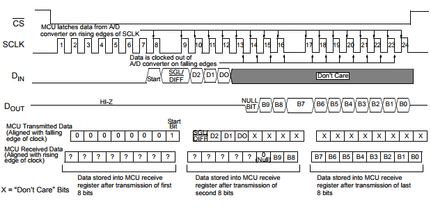
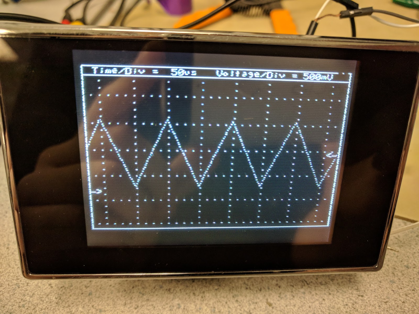
The accuracy of the oscilloscope is hard to quantify. However, when compared against the commercial oscilloscope from Tektronix, it is impossible to tell the error in human’s eyes. Therefore, we assert the accuracy of our oscilloscope is satisfactory. Below is a few comparison. Note the function generator we used to generate the signal input does not have precise frequency and amplitude control. Therefore, instead of comparing the TV screen against the nominal properties of the waveform, compare our oscilloscope with the commercial oscilloscope.
Figure 6. Our Oscilloscope with ~10KHz Triangular Wave Input
Figure 7. Commercial Oscilloscope with the same ~10KHz Triangular Wave Input
Figure 8. Our Oscilloscope with ~20KHz Sinusoidal Wave Input
Figure 9. Commercial Oscilloscope with the same ~20KHz Sinusoidal Wave Input
Here is an example of how the configurable parameters are helpful in examining waveform input:
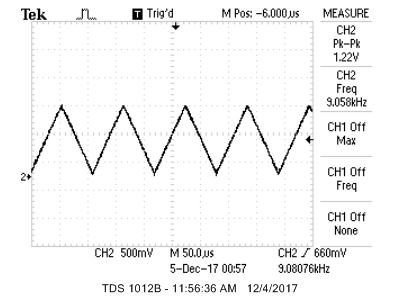
A Waveform that has to low frequency and amplitude to be shown in 50us-500mV window:
Figure 10. ~1kHz Triangular Waveform in 50us-500mV window
The same waveform can be clearly analyzed in a 500us-250mV window:
Figure 11. The Same ~1kHz Triangular Waveform in 500us-250mV window
The design process is safe for us designers, no soldering, high-voltage or large-scale mechanics involved. However, we paid extra care to protect the electronic components as we are dealing with mixed-signal. We always operate on a static-free station. Before feeding any signal input into PIC32, we check if the input is larger than 3.3V in commercial oscilloscope. The project is self-contained and had no interference with most other people’s designs, yet our project can be vulnerable if a static charge source is nearby. Our oscilloscope is very easy to use for someone with some electrical engineering background, yet I failed to even inform my friend from business school what an oscilloscope is.
For the purposes of our proposed project, we were able to accomplish all that we set out to do. Our oscilloscope was able to operate accurately across a wide time range. The output on the TV looked fluid and smooth. All in all, we consider our project a success.
In terms of future work, there are a lot of features that could be added on to our project to further improve the oscilloscope. Other operating modes such as FFT mode and slow-time continuous mode could be implemented on top of our project. In addition the ability to output the data in a format other than the NTSC standard would make an interesting extension to our project as well.
In addition to adding new features, work could be done to remove some of the constraints in our oscilloscope operation. Currently, the safe operating voltage range is between 0V and 3.3V. Work could be done to expand this voltage range further.
NTSC
In order to output our data from the oscilloscope on a TV, we needed the data to conform to the NTSC standard used in closed-circuit TV in North America. We accomplished this by heavily referencing Professor Bruce Land’s previous work.
In making this project, we took special care to make sure that we made all ethical considerations and conformed to IEEE’s Code of Ethics. One of the biggest concerns we had was safety. In working with electric circuits, we dealt with the dangers of damaging not only the device and fragile electrical components, but also the users of our device. In order to alleviate this risk, our device operates only at safe voltage ranges (0V to 3.3V). The device also has an easily accessible power switch provided by the PIC32 that can be used to shut down the device in case of emergency.
In our pursuit of this project, we also sought out honest criticism of our work throughout the design and implementation process. By consulting Bruce Land as well as the TAs in this course, we strove to create our device with as few errors as possible. To improve the understanding by individuals and society on the capabilities of our project, we extensively documented as well as made available the work and code that went into our device. We acknowledged Professor Bruce Land in all prior work that contributed to our final project.
Finally, we sought to report our findings as accurately as possible. In all the work we did throughout this project, we represented all data as accurately as we could. This report, as well as the weekly progress reports we submitted throughout the project, all reflect our work described to the best of our ability.
There are no reasonable legal considerations for this project
We appreciate and acknowledge the work done by Professor Bruce Land on his NTSC Video Interface. His code was referenced and used to help generate the NTSC Video that our oscilloscope outputs to the TV display.
While we found several oscilloscopes that can accurately read voltages and display their output on a TV screen, the only project that we found which used the PIC32 is the project made by Bruce Land that we referenced throughout our work. However, our project is different from his previous work in that it adds several new features to improve his previous work, including the ability to change the time/div, as well as the low-frequency mode.
We do not foresee any patent opportunities for our project.
The group approves this report for inclusion on the course website.
The group approves the video for inclusion on the course youtube channel.
Our code contains two files:
ascii_characters.h - Header file for interfacing with the TV to draw ascii characters
PIC32_TV_256x200_30Hz_scope.c - Main program file
Figure 12. Schematic
Cost
Total is $37.5
Main oscilloscope functionality
PIC32 ADC10 Configuration
PIC32 Timer Configuration
PIC32 DMA Configuration
Rotary Encoder Integration
Potentiometer & MCP3004 Integration
Improving Graphical Interface
Main oscilloscope functionality
PIC32 Timer Configuration
PIC32 DMA Configuration
Final Report Documentation
Software Libraries:
The NTSC video library, as well as a basic version of the scope, is borrowed from Professor Bruce Land at Cornell University: http://people.ece.cornell.edu/land/courses/ece4760/PIC32/index_NTSC_video.html
PIC32 Peripheral Libraries for MPLAB C32 Compiler:
http://ww1.microchip.com/downloads/en/DeviceDoc/32bitPeripheralLibraryGuide.pdf
Datasheets:
PIC32MX250F128B Datasheet:
http://www.microchip.com/wwwproducts/en/PIC32MX250F128B
PIC32 hardware manual sections:
http://people.ece.cornell.edu/land/courses/ece4760/PIC32/index_Ref_Man.html
MCP3004 Datasheet:
http://www.microchip.com/wwwproducts/en/MCP3004
Rotary Encoder Sparkfun COM-09117 Datasheet:
https://www.sparkfun.com/datasheets/Components/TW-700198.pdf
Potentiometer Sparkfun COM-09288 Datasheet:
https://www.sparkfun.com/datasheets/Components/General/Linear-Trimpot.pdf
Standards:
NTSC Standard: http://www.ntsc-tv.com/
Vendor Sites:
Digikey: www.digikey.com
Sparkfun: www.sparkfun.com