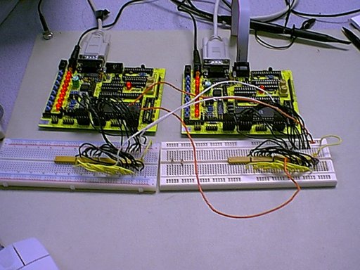
We thought it would be interesting to try and construct a simple modem out of the ATMEL 8535. The main motivation for doing this was to test some DSP theories about the effects of transmission power, noise, and modulation technique on the bit error rate. Initially, we wanted to connect our modem to the public telephone network; however, the voltage, current, and bandwidth constraints over a phone line would have made the project much more complex. Instead, we chose to use a simple wire channel, and focus our efforts on actually transmitting and receiving the signal waveform.
Our goal was to make our modem so that it would be full duplex and we would be able to send and receive characters over a noisy analog channel. For simplicity, we chose to use the UART and Hyperterminal on a PC to provide data to the modem, and display the output of the receiver. The characters were to be transmitted pseudo asynchronously by transmitting a high voltage synchronization pulse, one parity bit, then the eight data bits. This allowed for a high level of fault tolerance because the transmitter and receiver are synchronized at the beginning of every byte. Binary ‘1’s were to be transmitted by a waveform with values defined in a table so that we could easily change the waveform. To transmit binary ‘0,’ we simply negated the values in the table. We varied the number of samples per bit transmitted as well. To receive the signal the MCU waits for expected high voltage of the sync pulse. It then waits for the end of the sync pulse to begin sampling the bits. The reciever uses a correlator algorithm to detect whether the received signal was a binary '0' or '1.' We varied the number of samples per bit to evaluate the tradeoffs between speed and noise tolerance.
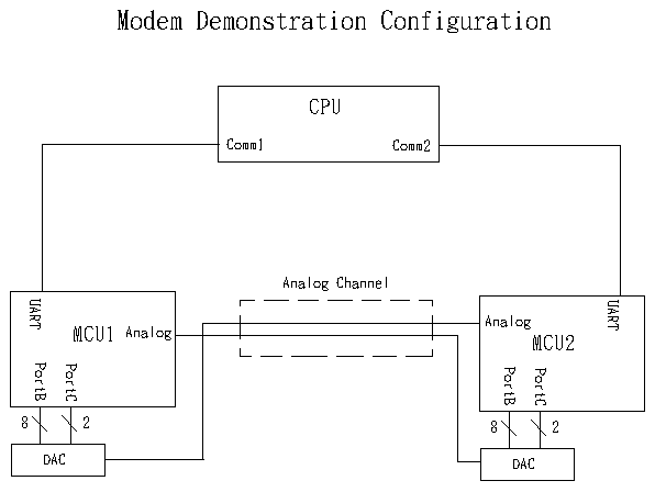
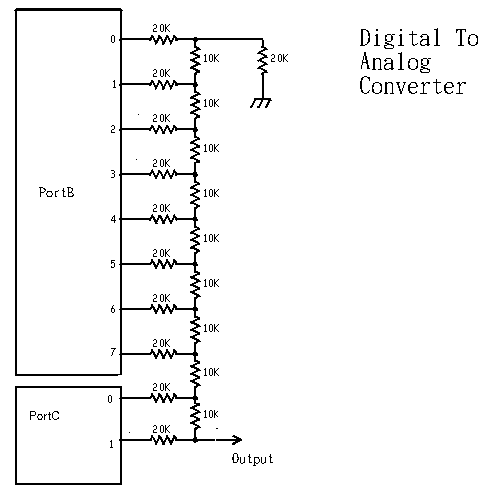
When a byte is received from the UART, the transmitter starts the transmit sequence begins by with a sync pulse. This is a short spike of five volts that signals to the receiver that a byte is coming. Following the sync pulse, the transmitter calculates a parity bit to ensure that the number of ‘1’s transmitted is even. The parity bit is transmitted as a waveform over the channel, followed by the eight data bits. To control the speed of the transmitted, we used the timer one compare match interrupt. Every interrupts, a new sample of the waveform corresponding to the bit is loaded from flash and sent to the DAC. Since we were using BPSK, we only needed to store one waveform in flash, since we could just negate the value to produce the waveform for a binary zero. Also, since we didn’t want to deal with negative voltages, we introduced a digital DC offset into out transmission. The DC offset was added to the value to be transmitted at the transmitter and subtracted at the receiver. This allowed us to avoid the added complexity of more external hardware, while still being able to use BPSK.
At the receiver, we sample the channel periodically using the timer one compare match interrupt to control the timing. When the analog to digital conversion produces a value the is in the range of the sync pulse, we know that a new byte will arrive at the next sample period, and we reset all of the counters that control where we are within the process of receiving a byte. In the sample period after the sync pulse, we take the sampled value and subtract off the artificial zero level, and multiply the result with a value that comes from flash. This value from flash is one of the samples of the transmitted signal. The result is then added into a sum register. This is the basis of the receiver algorithm that determines whether a waveform corresponds to a ‘0’ or ‘1.’ After eight samples, we check the sign bit of the sum. If the sign bit was ‘1,’ then the sum was negative, indicating that a zero was transmitted. If the sign bit was ‘0,’ then we interpret the signal as a binary one. We then had two registers that acted as a bit buffer to store bits as they arrived. After receiving each new bit, we shifted the registers to the left.
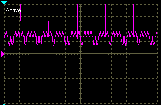
Waveform of "101110011"
After receiving nine bits, we did a parity check on the bits by counting the number of ‘1’s we received. If the number of ‘1’s was odd, then an odd number of bits were received incorrectly. Finally, we wrote the eight data bits to the UART.
Since the modem was full duplex, each modem had to both transmit and receive at the same time. Merging the two pieces of code became the most difficult part of the project, as we had to preserve the timing, and make sure that the two functions did trample over each other. To do this; at every sample period we transmitted the new waveform value first because the transmit code is short. All we had to do was transfer the sample value to the output ports. The amount of time that the receive code took was variable but always long, since the amount of processing depended on what part of the receive cycle the micro-controller was in. For instance, at the last sample period of the last bit, the receiver has to do an analog to digital conversion, an eight bit signed multiply, a parity check, and write the byte out to the UART. This sequence of actions proved to be the limiting factor in the speed of our modem.
In the presence of noise, there is always the possibility that the receiver will not correctly identify a bit. This error is a function of the energy of the transmitted signal. The larger the signal energy, the less likely the receiver will confuse a ‘1’ for a ‘0,’ or vice versa. In order to measure the probability of error for our modem, we appended a parity bit to each transmitted byte. This allowed us to empirically measure the probability of an odd number of bit errors out of the nine transmitted bits. We could then interpolate the probability that a single bit was in error. We were interested in calculating the probability of error as a function of signal energy by varying the shape of the signal. In our code, we had registers that kept track of how many bytes were received, and how many of those bytes failed a parity check. We intented to use this to produce a plot of error probabilty as a function of signal energy, but we ran out of time, and were not able to perform these tests.
The fastest we were able to reliably transmit was when we set one sample period to be 1000 clock cycles. Since our signal waveforms contained eight samples, this resulted in a transmission speed of 2 msec. per bit, or 500 bits per second. When we attempted to speed up the modem by decreasing the sample period to 500 clock cycles, the result was unreliable transmission. From looking at our code, we suspect that this is due to the fact that the code required to receive data took longer than 500 clock cycles. This means that the transmitter begins to send a new bit before the receiver is done processing the previous bit. At 500 bits per second our modem pales compared to modern modems, which can obtain throughputs two orders of magnitude better. We did; however, manage to outperform a 300 bps modem ignoring any sort of bandwidth analysis.