PROGRAM/HARDWARE DESIGN
Because of the large number of scenarios that need to be checked in the AI for both levels two and three, this section of the program was relatively hard to develop and test. Debugging this code is also problematic: on top of writing code for a large number of situations, we must also test that those situations work. Often, after days of testing and gaining no indication that the program still had bugs, we would come upon a situation which we had not seen before, and then would have to comb through the code in order to discover the bug. Developing weights for various situations in the hardest level such that an optimal strategy could be reached was also difficult. We attempted to derive these weightings theoretically, but relied mostly on intuition. In the end, the weights were based upon a combination of common sense, intuition, and trial and error. The STATE MACHINE provides a good example of the design of the program. We did have some problems with our randomizing schemes (an AI strategy which only puts checkers into one column is easy to beat). Initially, we attempted to use the on-board timers to generate random numbers, but ran into problems which we could not easily resolve. We ended up using a simple random number generator found on How Stuff Works
The hardware schematics below show the layout of our hardware. We actually spent three hours early on in the project attempting to debug major problems which were occurring with the keypad. After re-mapping our keypad lookup table based upon the erratic results which we were receiving (and pulling more than a few strands of hair out of our heads) we realized that our board was bad, and the problem was fixed simply by switching boards. Again, most of this hardware design stemmed either from what was accomplished in previous assigned labs or from what was found on the class website.
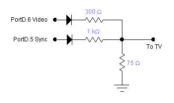
Schematic 1 for generating NTSC video signals
from digital I/O image adopted from Professor Land
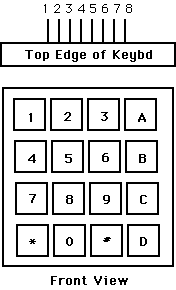
Pin 1  -- row 1 2 3 A
Pin 2  -- row 4 5 6 B
Pin 3  -- row 7 8 9 C
Pin 4  -- row * 0 # D

Pin 5  -- col 1 4 7 *
Pin 6  -- col 2 5 8 0
Pin 7  -- col 3 6 9 #
Pin 8  -- col A B C D

(a) Each switch shorts one row to one column.
(b) Each pin should be connected to one bit of an i/o port.
(c) The i/o port pins will be used both as inputs and outputs.
    When they are inputs, they should have active pullup resistors.
Schematic 2 for inputting keypad
to digital I/O image adopted from Professor Land
As mentioned earlier, we did not actually attempt color television because we could not secure an actual television until it was already too late to purchase the other parts (e.g. RGB to NTSC encoder), since the lead times were too long. Of the three companies which parts were being ordered from, none sold the hardware that we wanted for color television. Other companies that we looked into had lead times over one week.
We also spent several hours attempting to use interlaced frames in our project. Currently, we write one entire frame at a time – every line is written in one frame. With interlaced frames, only every other line is written per scan of the screen. This is advantageous from an animation standpoint. However, all of our attempts were met with either two images on the screen, or a ridiculous amount of flicker. In the end we determined that our project did not use intense animation and thus would not benefit from interlaced frames and thus we abandoned this goal.