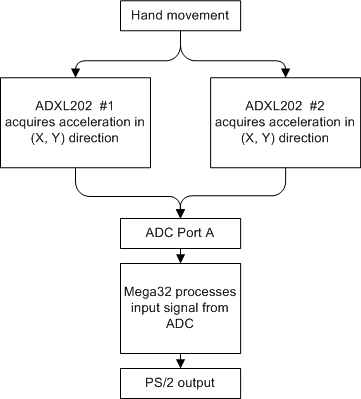
High Level DesignThe hardware design block diagram of our gMouse will be as follows
The MCU will generate output signals according to the PS/2 standard protocol. There are two output pins, the first one is DATA, and the second one is CLOCK. In the PS/2 protocol, the device will drive the CLOCK signal. Both the CLOCK and DATA will float default at VCC. During transmission, the mouse will drive the CLOCK and DATA lines. The PS/2 protocol requires the device to send clock between about 10 kHz to 16 kHz. In our specific implementation, our clock speed is 12.50 kHz, which is about 60 microseconds per clock cycle. The host can inhibit device transmission by pulling the CLOCK signal low for more than 100 microsends. The host could pull the CLOCK signal low for two reasons: one is to inhibit transmission because the host is processing data, and the other is to request to send information to the mouse. In the second case the host will pull the DATA line low to generate a start bit and wait for the device to generate the clock signal. More information on the PS/2 protocol can be found on http://govschl.ndsu.nodak.edu/~achapwes/PICmicro/.We also uses three ports on the MCU for ADC conversion. This is similar to the digital thermometer lab. We hook up the analog output from the chip, which is soldered to a PCB provided by the professor. The software design on the MCU will be as follows:
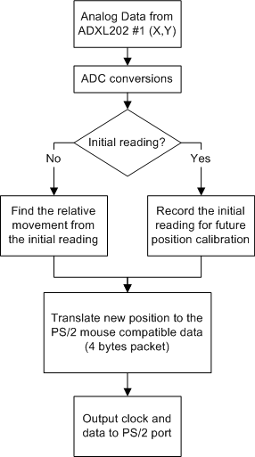
Our software will measure the ADC input and convert it to PS/2 mouse data packets. First, we will introduce the PS/2 protocol. A PS/2 byte has 11 bits. (A) 1 start bit. This is always 0. (B) 8 data bits, least significant bit first. (C) 1 parity bit (odd parity, 1 when number of bits is even). (D) 1 stop bit. This is always 1. On a device-to-host transmission, the keyboard/mouse writes a bit on the Data line when Clock is high, and it is read by the host when Clock is low. The host-to-device is request or transmission is a little more complicated. The host will pull the clock to ground for more than 100 microseconds, and then the host will bring the data line low to signal a start bit. Then the host will start waiting for the device to generate a clock signal, the host will send bits of data to the device based on the device generated clock. The device should expect to receive the initial start bit, 8 data bits, a parity bit, and a stop bit. The data bits are valid for the device to read when the clock is high. The device is also expected to generate an ACK bit back to the host after receiving the stop bit, and the host should be able to read the ACK bit when the clock is low. There will be more detailed information on how we implemented the PS/2 protocol in the program design section. |