|
|
|
|
05/02/05 |
|
|
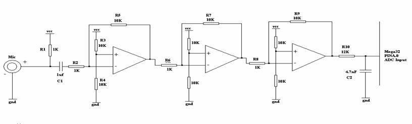
Program and Hardware Design Microphone Circuit We started out our project by designing a filter and amplifier for the microphone. The following diagram shows our design.
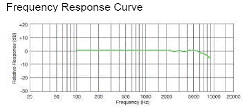
This circuit can be divided into four parts, microphone, high pass filter, 3 stage amplifier and a low pass filter for easy understanding. Unlike the common 3 pin versions (vcc, gnd and output) our cheap microphone (Model Number: MD9745APZ-F) had two pins one for ground and one for output. Since there were no vcc we had to pull up the output using a 2.2K resister to the vcc of 5V to provide current for the microphone. Microphone had constant frequency response from 100Hz and an upper frequency 3db cutoff at around 6Hz. This was more than enough for our voice recorder since human voice was in the range of 150Hz to 4kHz. The frequency response of the microphone is given bellow.
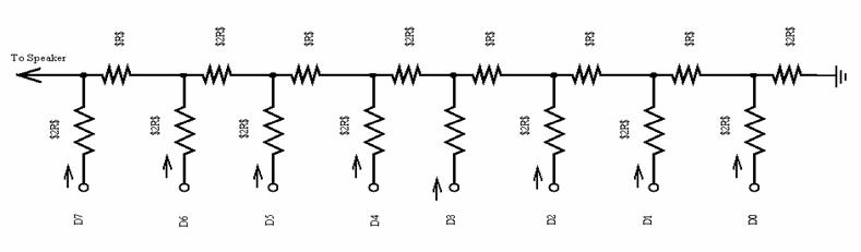
The next stage is the first order RC high pass filter and it is built by a 1uF capacitor (C1) and a 1kΩ resister R2 in series. The cut of frequency of this high pass filter is at around 160 Hz which is close to the lower limit of human voice spectrum. The base frequency of the human voice is around 400Hz. This filter cuts off the 60Hz noise from the surrounding electronic equipments while passing in human voice. It also cuts of DC to give us a pure signal. In the next part of the circuit this signal is amplified using three identical non inverting amplifiers. These amplifiers are built using LMC7111 opamps. We are running these opamps using +5V and Ground power supplies rather than +/-5V supply voltage. The reason for this is that we can only sample 0 to 5V using the mega32 ADC. The gain is set by R2 and R5 (R5/R2) for the first stage and R6 and R7 for the second stage(R7/R6) and R8 and R9 for the third stage (R9/R8). Resisters connected to v+ of the opamp are for offset. This is done to ensure that the final output signal is centered on 2.5V which will represent 0V signal in ADC. The third part of the circuit is a simple first order RC low pass filter which is made of R10 (12KΩ) and C2 (4.7nF). The cut off frequency of this filter is 2821Hz which is above the common human voice of 2000Hz. The Nyquist frequency for 2821hz is 5642 which is way bellow the sampling frequency of 8Kz. Thus this filter reduces aliasing. The next step in our project was writing code for the Mega32 ADC. This was very simple and closely resembled old lab projects. Since we were only planning to sample at 8bits per sample we only read from the ADCH register. We read from ADCH in timer0 interrupt which fired at 8kHz, our sampling frequency. To test this we stored these values in eeprom and outputted to the LEDs in STK500. We were only able to store ¼ th of a second in eeprom. DataFlash Interface: Some of the STK500 boards in the lab had a 2Mb DataFlash embedded in it. We used Serial Peripheral Interface (SPI) protocol to talk this DataFlash. It consists of 1024 pages of Main Memory, with 264bytes per page. I also had two, 264byte buffers. Opcodes must be sent to the DataFlash through SPI mode to send or receive data from the Dataflash. A message is be sent in the following format: 8bit opcode, 24 bit address, (8 or 32) bits of data. The fact that DataFlash had two buffers was very useful for us since our data was very time sensitive. It took longer than 1 sample period to write a whole page from buffer to the memory and vise versa for reading. So we had to alternate between buffers when we were sampling and playing back. That is when we sampled we wrote our samples into one buffer while the other buffer was being written into the memory and vise versa. This enabled a smoother sound rather than a clipping noise when only one buffer was used. DAC: Another main part of our project is the 8 bit D/A converter (DAC) using Ladder Resister Network. A Diagram for it is given bellow. We used more accurate 10K and 20K resister dips to build it since accuracy was very important. We got very close to 20mv division for a change in bit. We drove the output of the DAC through a high pass filter to smooth out the signal and a low pass filter to reduce the 60Hz ringing.
LCD User Interface and Options: Or voice recorder was controlled in program by a state machine. When butter0 is pushed we changed state to the record mode were we record into a track. We record as long as the button is pushed or we run out of memory. The lcd will display how many tracks you have written so far. Button1 is pressed once to play back the current track and pressed again to stop. While not playing, you can press button2 to move down or button3 to move up on track list. The current track will always be displayed on the LCD. By pressing Button2 or Butten3 while playing back, you can change the playback frequency and get cool deeper voice or Chipmunk like high pitched voice. Things that almost worked: We tried to interface the microcontroller with an SD card using SPI mode but we failed since our single SD card holder’s pins broke off. By the end of the hard holder’s death we were able to initialize and read many many sectors. But read/write time between sectors was unacceptably large. It required a 1ms delay when sending or recovering a sector. We tried to make this nonblocking but putting it outside the timer0 interrupt where the sampling and play back was at, but it failed to read sectors this way. Another thing we tried is Adaptive Differential Pulse Code Modulation (ADPCM) and Down Sampling to attain lesser bit rate. The results of these experiments were pretty disappointing due to high noise. ADPCM stores the encoded difference between current sample and encoded earlier sample and plays it back by decoding the 4 bit number using an adaptive step size. Our implementation of this was not correct, since we generate huge amounts of noise. If we had not spent such a high percent of our time on SD card implementation, ADPCM may have been a nice addition. We tried several other simpler algorithms, but the noise levels made them not worth implementing. These included storing the average of every two pulses. This created a smudging effect, so we added code that sharpened the peaks. However, the noise was still fairly high. We also tried to playback at twice the speed that we recorded. The purpose of this was to generate more samples. Another method we tried was truncation of the bottom four bit, so that two samples could be store per byte. These are just general things that we tried. We tinkered around with the various thresholds that we used. We also tried several combinations at the same time. However, none of these methods produced a clean enough signal to record. Thus we stayed with the original sampling frequency, and 8 bit samples. References: Dataflash.c and Dataflash.h files we used for SPI mode communication with the DataFlash was pointed out to us by our TA Chethan Pandarinath.
|
This site was last updated 05/02/05