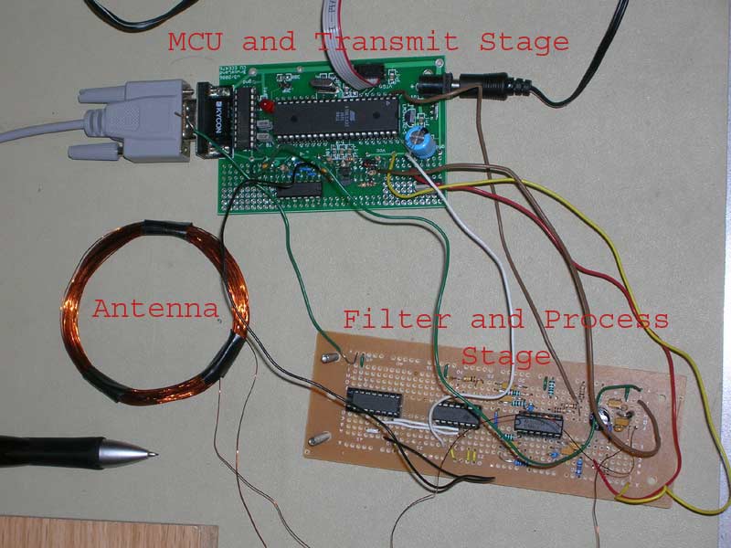
By: Craig Ross (cjr37) and Ricardo Goto (rhg22)
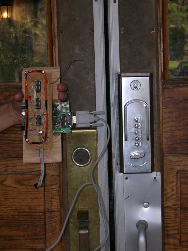
For our final project, we designed and built (and exhaustively tested) an RFID-based proximity security system for use with Cornell Identification cards, which have been RFID-embedded since fall of 2003. The idea for this project was sort of spawned from our general interest in RFID technologies and the near-simultaneous occurance of Lab 2 (Keypad Security System) and the antiquated lock system at our fraternity house breaking.
"Old and Busted...New Hotness" -Will SmithAt the highest level, our device uses an antenna coil to power the RFID tag embedded in our Cornell ID's and read the induced response from the card. This response is then filtered and manipulated into useful data and interpreted by the Atmel Mega32 microcontroller which runs the actual security program. In addition to interactions with the ID cards, the system is in contact with an administrator computer via a serial communications link and hyperterm. The security system can store up to 20 45-bit codes which are derived from communications with each unique RFID tag. If a card is read and it is not in the code database, a red LED flashes for 3 seconds. Likewise, if the code can be found in the database, a green LED lights for 3 seconds. From hyperterm, the administrator has the power to add codes, delete codes, list all codes, "unlock" the door (the equivalent of the green LED flashing), and initialize routines which allow codes to be added to the database by gathering data from the reader itself.
Educational topics explored in this lab include (but are not limited to) passive filter design, active filter design, amplification circuits, RF antenna design, digital logic, serial communications, RFID theory, pin interrupts, timer interrupts, and soldering. In short, for this project we used elements of basically every introductory level ECE course we have taken. Since we are dealing with such a complicated topic, on the hardware side of things we tried to rely as much as we could on proven circuit designs. This would enable us to focus more on getting our system working well as a whole rather than spending countless hours debugging small parts of our project. For this, the Microchip® microID 125 KHz Reference Guide (see citations section) proved to be an invaluable resource for both theory and results.
Before we start with actual circuit design, it is neccessary to understand the principals behind the technology that this project has set out to harness; passive RFID communications. Passive RFID tags work in such a way that they are actually powered by an external signal, which, in most cases is the carrier signal from the tag reader circuit. These tags are fairly simple and are comprised of merely an L-C antenna (similar to the one shown in the block diagram below) and the circuitry neccessary to modulate this carrier signal once powered on. The reader and tag communicate using magnetic coupling since their respective antennas can sense changes in magnetic field, which is observed as a change in voltage in the reader circuit.
The Cornell ID cards we use in this project were developed by HID®; specifically the HID DuoProx II cards. These are useful because they have both embedded RFID as will as a magnetic strip, while much of campus is starting to switch over to proximity entry systems, many current systems (including the dining halls) are still swipe-operated. From looking at their website, it was difficult to determine much information about the card's operation, asside from the fact that it operates at a 125 KHz carrier frequency and it could have a tag size anywhere between 26 and 128 bits long.
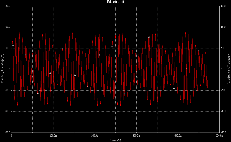
After many hours of research we discovered that the modulation type used in the cards is Frequency Shift Keying (FSK), one of the more common ways used in RFID. FSK modulates the signal by essencially multiplying a lower amplitude, lower frequency signal with the carrier signal, creating an AM-like effect; the lower frequency enveloping the carrier frequency. To switch between a "1" and a "0", the tag switches the modulating frequency. The two frequencies used by our cards were 12.5 KHz (125 KHz/10) and 15.625 KHz (125 KHz/8), which correspond to 1 and 0 respectively. The modulation produces an effect that looks similar to the figure below:
Figure 1: Simulation of FSK Modulation With Modulation Frequencies of 12.5 and 15.625 KHz and Carrier Frequency of 125 KHzThe job of the reader circuit is to provide the 125 KHz carrier frequency, transmit that to the tag, and detect the magnetic coupling from the tag, which should look like the figure above. In order to interpret this data, the carrier frequency must be removed, and the enveloping frequencies must be magnified into something measureable.
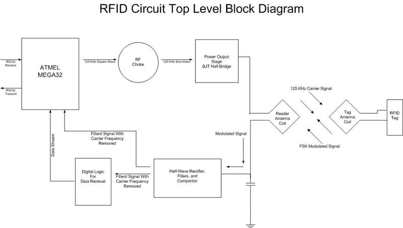
The block diagram/flow chart for our reader circuit can be found in the figure below:
Figure 2: Block Diagram of Our CircuitAlthough each individual part of the circuit and program will be described in detail later, the general idea for circuit operation is as such: The Mega32 provides a timer-driven 125 KHz square wave for our carrier frequency. This is then sent through an RF choke, which is essentially a passive low-pass filter with steep drop-off to knock out the upper harmonics and leave us with only a sine wave. The sine wave is then amplified using an emmitter follower PNP transistor and a half bridge to maximize current. Since our resonant circuit is a series L-C circuit, maximum resonance is achieved at minimum impedance, so it is very important that we provide adequate current amplification as to not overdrive our microcontroller. To help reduce the strain (and ramp up the current more) further, the square wave output from the MCU is put through parallel inverters.
On the recieving end, the signal is first half-wave rectified, since the negative part of the signal doesn't really make a difference, and is then fed through a half-wave R-C filter to help knock out most of the 125 KHz carrier and detect the envelope signal. This signal is then bandpass filtered using a series a Twin-T active bandpass filters, and lowpass filtered with an active Butterworth filter to further decrease gain in frequencies outside of the 10-20 KHz area and increase gain of the envelope signals such that it saturates the op-amps of the filters. As a final stage the signal is put through a comparator and resistive divider to produce a nice square wave at logic levels. Some D-flip flops and a decade counter are used to extract data from the modulating square waves. Which are fed into the MCU and processed.
Hardware and Software Tradeoffs:
There are many ways to design a proximity card reader in terms of tradeoffs between hardware and software. In most cases, software is cheaper because you don't need to purchase any parts but at the same time you are costing the MCU processing time. Using more hardware will obviously increase the cost of the design but ultimately may alleviate painfully tedious optimizations that would have been necessary had you used code to replace a component or device.
One of the first tradeoffs we encountered was whether to use the Mega32 or a separate counter to generate the 125 kHz carrier frequency. The microID 125 kHz RFID System Design Guide suggested using a 14-stage binary counter to divide the clock from the crystal to 125 kHz. However, since the Mega32 has built-in hardware timers that can output to one of the pins, there was no need to use a counter.
Another tradeoff we encountered was whether to use DSP or hardware to analyze the signal on the antenna. Recall that this signal is the carrier signal and the magnetically coupled response from the card superimposed onto each other. Using DSP, we could sample at the Nyquist frequency and compute the FFT of the signal to find what frequencies are present in the response and from there decode the response. If we were to use DSP, we would have to sample at greater than 250 kHz meaning there would only be 64 cycles between samples to compute the FFT. This imposed a huge constraint on the rest of our security system so we decided to implement the most of the decoding in hardware.
Transmit Stage: RF Choke and Power Amplifier:
The circuit of Figure 3 below is an RF choke followed by a current buffer and half-bridge amplifier. The RF choke is used to filter out most, if not all of the upper harmonic frequencies found in the square wave output from the MCU, leaving the fundamental frequency, 125 KHz, as a sine wave to be amplified. The square wave generator seen in the figure below is, in actuality, the output from the MCU and a set of inverters to ramp up the current. Diodes are used in the half bridge to help reduce crossover distortion caused from differing points of either transistor in the half bridge turning on and off. In our design we used the 2N3904 and 2N3906 NPN and PNP BJT transistors from the lab since they were cheap and convenient. In order to get better amplifier gain, and thus increase read range of our circuit, we could have used power MOSFETS instead for the half-bridge, but we found the BJT's gave us a mostly acceptable level of gain, especially once the circuit was tuned.
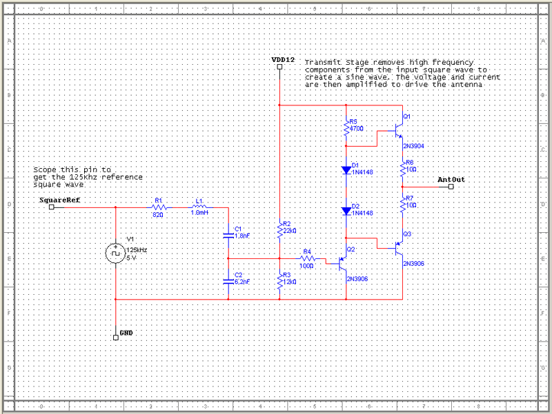
Figure 3: Circuit Diagram for Transmition Portion of Circuit
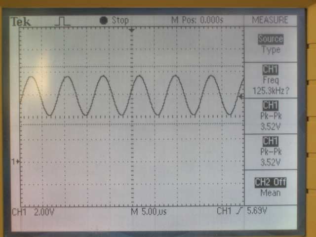
Figure 4: Oscilloscope Reading of Transmit Stage OutputResonant Antenna Circuit:
While this portion of our circuit is only comprised of two components, it is also arguably the most important hardware element; if it performs poorly then our security system performs poorly. Because this design was recommended for proximity solutions from the Microchip® guide, we decided to go with a series L-C resonant curcuit as opposed to one where the resistor and inductive antenna were in parallel. Because of this, at maximum resonance we also observe maximum current. In order to determine values for the inductance and capacitance needed, we used the equation:
, where f is the resonant frequency (in Hertz), L is inductance (in Henries) and C is capacitance (in Farads). Since f = 125 KHz and we had plenty of 1 nF ceramic capacitors in the lab, we settled on an inductance of 1.62 mH.
Figure 5: The different Pieces of Our Circuit Before we Constructed the Final Form FactorTo construct an antenna with the neccessary inductance we used coils of laquered copper wire, since it works well and is fairly compact. In our final construction revision, we used a rectangular-shaped antenna coil since it fit well with the design. The figure above shows the coil as circular, which is what we used for most of our preliminary testing before we actually put the unit together. Both antennas operated roughly the same as each other, although the rectangular coiled one resonates more. Inductance for the rectangular coil is determined by the following equation:
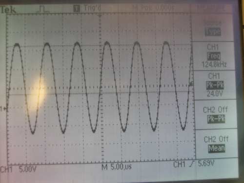
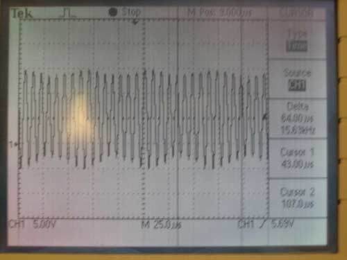
, where L is in microHenries, x and y are the width/length of the coil (in cm), h is the height of the coil (in cm), b is the width across the conducting part of the coil (in cm) and N is the number of turns. In our case, x=3.6cm, y=13.8 cm, h=1 cm, and we estimated b=.3 cm. Using the equation, we calculated the coil to need approximately 90 turns. It turned out this was a pretty good estimate. After constructing the coil, we proceeded to tune it by removing coils until we saw the highest resonant voltage from our carrier frequency, which was at roughly 88 turns. Oscilloscope results from this circuit, with both just the carrier frequency, and with the modulated signal from the RFID tag can be seen below.
Figure 6: The Carrier Signal in the Resonance Circuit (left), and our Modulated Carrier Signal When an RFID Tag is Placed Near the Antenna (right)
Half-Wave Rectify and Filtering:
This portion of the circuit is devoted to separating out the carrier frequency from the modulating envelope, since its really only the envelope that has the data we care about. The first stage is half-wave rectifying the signal to make things simpler and then filtering it slightly with an R-C filter. As is the norm for filtering AC signals in this manner there is some 125 KHz ripple, but choosing good values we could make the enveloping frequencies stand out from the ripple. For this we chose R=390 KOhms and C= 2.2 nF. Scope readings are shown in the figure below. Note that the peaks are the ripple, and the whole signal seems to oscillate at 15.625 KHz. You can tell this because there are 8 125 KHz ripple peaks per oscillation of the envelope. At a 12.5 KHz envelope, there would be 10 ripples per oscillation.
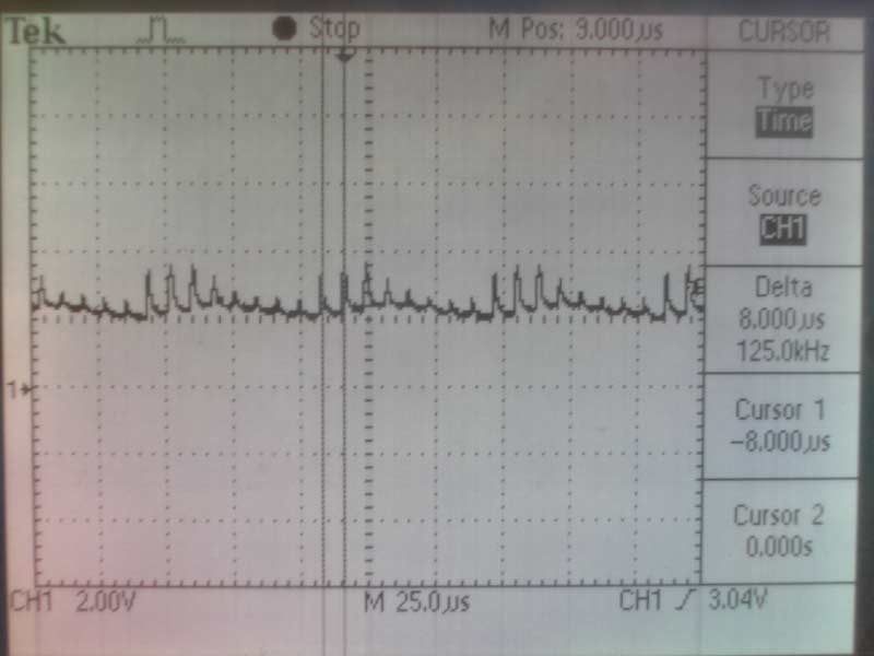
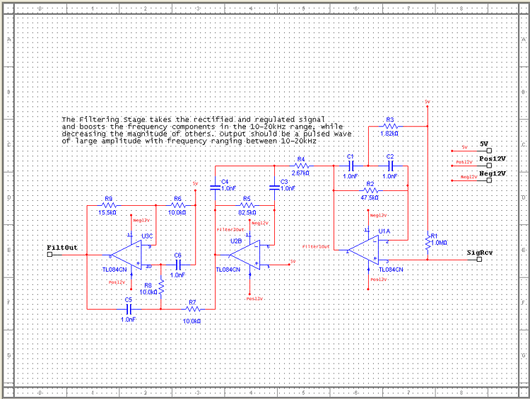
Figure 7: What the Signal Looks Like After the Half-Wave Rectify and First Round of FilteringOnce signal leaves this stage, it passes through a capacitor to knock out the DC offset and into the next set of filters; a pair of active Twin-T filters and an active Butterworth filter with the TL084 OpAmp as the gain element. The circuit diagram for this is in the figure below:
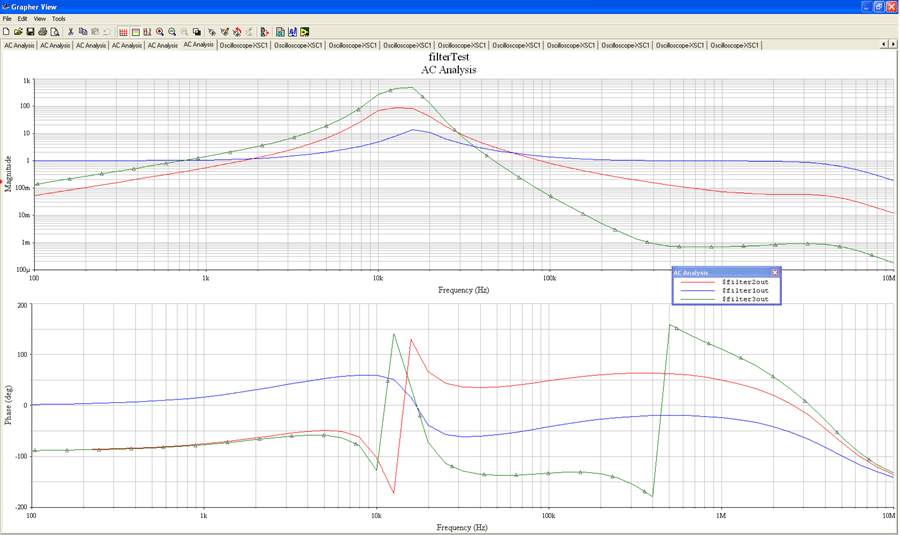
Figure 8: Circuit Diagram for the Filter Stage. Signal Comes in From the Right and Exits out the Butterworth on the LeftAs can be seen from the Bode Plot in the figure below, the first filter mostly isolates the pass band (10-20 KHz), with roughly unity gain for all frequencies outside the pass band. The second filter further accentuates gain in the pass-band while slightly reducing the magnitude of frequencies outside the pass band. After this, the signal goes through a massive Butterworth Low-Pass filter to drastically increase gain of lower frequencies already in the pass band and virtually eliminate the higher frequencies, including the 125 KHz carrier signal.
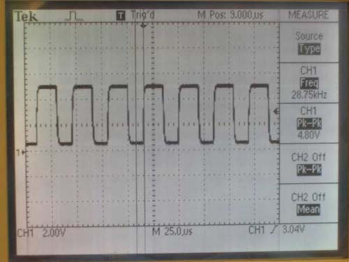
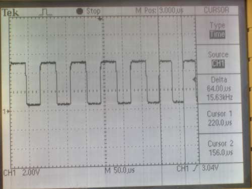
Figure 9: Bode Plot Showing Behaviours of All Three Active FiltersOnce out of the filters, the signal is then put through a TL084-based comparator and a resistive divider to generate a nice square wave at logic levels. The 12.5 KHz and 15.625 KHz frequencies come out of the filters beautifully. When no card is present, the system reports a 28.75 KHz wave which represents the highest frequency to come out of the filters with enough gain to saturate the opamps.
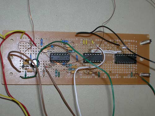
Figure 10: Protoboard With Our Filter Circuit (left) and 28.75 KHz idle Frequency From the Filter Output
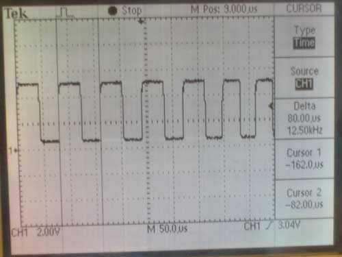
Figure 11: Envelope Frequencies After Filtering and Reduction to Logic Levels. 12.5 KHz is on Left While 15.625 KHz is on Right Data Creation Stage:
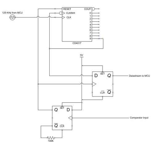
Technically, from the output of the comparator we should have been able to read and interpret data from the card using a timer interrupt. We quickly realized, however, that by doing this we would cripple the functionality of our system. In order to accurately measure the frequency of the incoming data stream we would realistically need to sample at 125 KHz, which means that, with a clock rate of 16 MHz we would have 128 clock cycles to compute everything before the next sampling interrupt fired. This would have been extremely difficult to implement. Looking for an alternate method to obtain data, we found a brilliant design in the Microchip reference guide, which makes use of flip-flops and a decade (Johnson) counter. This circuit can be seen in the figure below:
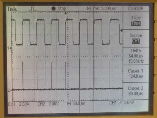
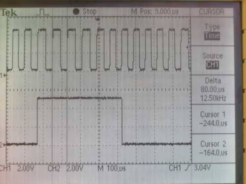
Figure 12: Circuit Used for Data GenerationThe way this works is as follows: The comparator output serves as the clock for the first D flip-flop, which also takes logic 1 as its D value. On the rising edge of the comparator clock, Q is immediately set to 1. However, simulataneously ~Q goes low and clears the flip-flop. This creates an extremely short pulse which serves as a reset for the decade counter and clock for the second flip-flop. The decade counter is just a 1-hot counter which takes a 125 KHz clock. With every rising edge of this clock, the counter outputs the next pin to logic 1; so typical output would look like (if one were looking at output pins 0-9 of the counter) 1000000000 0100000000 00100000000 etc. However, this counter is being reset with every rising edge of the comparator output. Thus, since we've already determined that 125 KHz/10 = 12.5 KHz is to be our frequency that represents logical 1, all we have to do is check for the output on pin9 to know whether or not we see that frequency. If the system is operating at either one of the other possible frequencies, the counter will be reset before pin9 can go active. The pin9 output serves as input to the second flip-flop and also to the clock inhibitor, which keeps the 9th pin high until the counter is reset. Because of this set-up, the Q output of the second flip-flop will remain logical 1 so long as modulating frequency is 12.5 KHz and will drop down to 0 if its anything else. Theoretically, this circuit should work perfectly. However, experimentally it did not, and thus required a small modification. The 100 KOhm resistor on the first flip-flop serves to lengthen the time it takes for the ~Q signal to get to CLEAR. Since all transistors have some amount of natural capacitance, this forms an RC circuit of sorts with a set RC time constant for the signal to rise or fall. As it turns out, this time was too short for the decade counter. The original design from the reference guide specified only a 10KOhm resistor between ~Q and CLEAR. With the 10 KOhm resitor, pulse widths for the reset pulse were a mere 50 ns long, while the counter required at least 250 ns. This caused some very eratic behaviour. After many hours of debugging, we finally pinpointed the problem and replaced the resistor with the 100 KOhm resistor which increased the pulse width long enough for the counter to correctly operate. The figures below show the behaviour of the circuit when operating correctly:
Figure 13: Comparator Output with Reset Pulse (left). Comparator Output with Data Output (right)
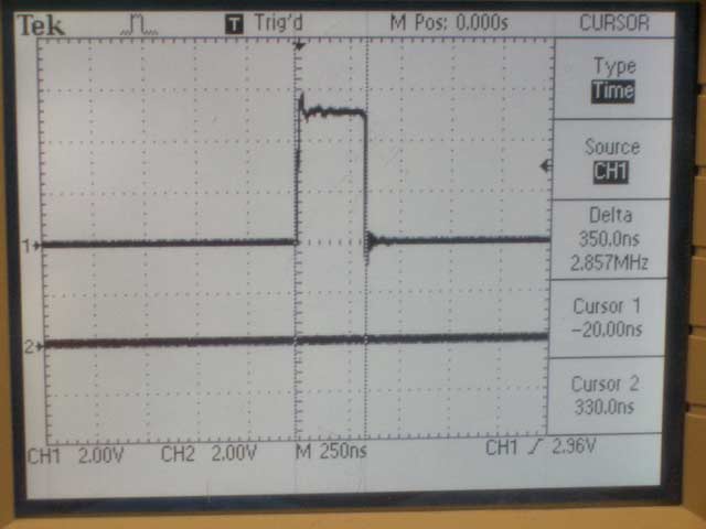
Figure 14: A Close-Up of our Reset Pulse Reveals That it is now 350 ns; 100 ns Over the Minimum for the Decade Counter
Software Design and Program Details:
Initialize:
This function initializes the various interrupts, timers, input-output, and global variables utilized in the program. The following are all initialized or setup here:
- Timer2 is used to toggle OC2 to generate a 125 kHz square wave.
- Port A is the output of the digital counter/flip-flop circuit.
- Port C is the LED output.
- Timer0 is used to count milliseconds for keeping track of time and controlling the timing on scheduled tasks and timer0 interrupt is enabled.
- Enable the transmitter and receiver in the USART and set the baud rate to 9600.
- Initialize flags, counts, buffers, and other state variables.
- External interrupt 2 is enabled and set to trigger on the rising edge.
- Set interrupt bit.
- Hold and prompt for the date and time before entering the while(1) loop.
USART Receive Interrupt
This interrupt handles any typed characters received from the terminal through the RS232 connection and stores it into a buffer. It also echoes the character to the terminal. Once a carriage return is detected, the receive-ready flag is set indicating that a line command has been entered by the user via the terminal.
USART Transmit Interrupt
This interrupt handles transmitting characters to the terminal. It simply loops through the transmit buffer until the last character is sent and then is ready for another transmission.
Timer0 Compare Match Interrupt
This interrupt serves as a timer to control the scheduling of different timers. It decrements the timers for timing how long the door is unlocked, timing how long a second lasts, and for checking the receive-ready flag.
External Interrupt2
This interrupt samples the data (output of the counter/flip-flop circuit). It is triggered by the rising edge of the output of the comparator. The output of the comparator is approximately a 29 kHz square wave if there is no modulation, and a 15.625 kHz or 12.5 kHz square wave if there is modulation. When the output of the comparator is 15.625 kHz the data is 0 and when the output is 12.5 kHz the data is 1. The point of this interrupt is to detect how many bits are in a 0 or 1 pulse of the data. Thus every time this interrupt fires, we increment a counter and add the sample to an array.
Main Method
In main, there are 3 major modes of operation. The mode of operation at startup is normal; however the modes can be changed through the terminal.
In normal mode, the reader waits for External Interrupt2 to finish reading a response from the card. It does this in about a thousand executions of the interrupt. When enough bits have been sampled, we turn off the External Interrupt2. When first analyzing the response from the card, we noticed periodicity every 540 bits. Thus, to guarantee that our sample window captures a full continuous 540 bit cycle, we sampled 1080 bits before turning off the interrupt. An example of a 1080 bit response looked something like this:
001111100000011111000000111111000000000000111111111100000011111000000000000111111000000111110000001111100000011111100000 11111100000011111111110000000000001111110000011111100000011111111110000000000001111110000011111111111000000111110000001111
00000000000011111100000011111111110000000000001111110000011111100000000000000000011111111111111110000011111100000011111000000 1111100000011111100000111111000000111110000001111111111000000000000111111111110000001111100000000000011111100000111111000000
111110000001111111111000000111111000001111110000001111100000011111000000111111000000000000111111111100000011111000000000000
1111110000001111100000011111000000111111000001111110000001111111111000000000000111111000001111110000001111111111000000000000
11111100000111111111110000001111100000011111000000000000111111000000111111111100000000000011111100000111111000000000000000000 11111111111111110000011111100000011111000000111110000001111110000011111100000011111000000111111111100000000000011111111111000000
1111100000000000011111100000111111000000111110000001111111111000000111111000001111110000There is a long sequence of 1's and 0's that stand out; we used these as references to identify the start and end of the 540 bit response. To extract the 540 bit response we wrote a function to detect a sequence of 15 to 18 1's. This function loops until it finds the start sequence and stores it in a global variable and calculates the end sequence.
There is also something noticeable about the 540 bit sequence. There are 1's and 0's in groups of 5, 6, 10, 11, or 12 excluding the start and stop sequence. Since 10, 11, and 12 can be made from combinations of 5 and 6, we hypothesized that maybe these longer groups are combinations of two groups of 5 or 6. With this in mind, we wondered whether a group of 5 or 6 bits possibly represents a single bit. This would make sense because the card cannot perfectly transition from one modulated frequency to another without some transition. Thus a group of 10, 11, or 12 represents two bits. Thus the reduced (90 bit) version of the 540 bit response excluding the start and stop sequence is extracted by detecting sequences of bits and replacing them with a single or a double bit:
010101010101011001101001010101101010101010011010010101010101100101011001011010100101100101
From this code, it is fairly obvious that the reduced sequence is encoded in Manchester code. If you split up the 90 bit response into pairs of bits, there are transitions within each pair:
01 01 01 01 01 01 01 10 01 10 10 01 01 01 01 10 10 10 10 10 10 01 10 10 01 01 01 01 01 01 10 01 01 01 10 01 01 10 10 10 01 01 10 01 01
A transition from low to high corresponds to a 1 and a transition from high to low corresponds to a 0. Since two bits correspond to a single bit, the Manchester decoded response has half the bandwidth and is thus only 45 bits long:
111111101001111000000100111111011101100011011
We believe this code is the raw data stored on the card. We have not been able to decode this further to find it's relation to Cornell student ID number but it is not necessary since this number is unique to each card. After decoding the initial 540 bit response to this 45 bit code, we store this data and sampled again. To prevent false reads, we keep sampling until we successfully read 3 consecutive identical codes. If we get 3 consecutive identical codes, we compare this code to the code bank (where all the authorized codes are stored). The code bank is stored in EEPROM due to limited space in SRAM. If the 3 consecutive identical codes match a code in the code bank, a green LED is lit for 3 seconds to signify that the door is unlocked. If the code does not match the code bank, a red LED is lit to signify that the door is not opened and that the code is not authorized. A statement is also printed to the administrative terminal providing the card code, whether the card was accepted, and the time at which the event occurred.
The other mode is called remote operation. In this mode, the admin has a choice of remotely adding a code to a specific code bank position or remotely adding any number of codes (bound between 1 and 20 inclusive). When adding a code to a specific code bank position, we turn on External Interrupt2 and read the card response. Just like in normal mode, we find the start code, reduce the sequence, and Manchester decode the sequence. We do this until we read 5 consecutive identical codes and then store it into the specified position in the code bank.
When adding a specific quantity of codes, we first search through the status of the code bank and find the first unused position. Then we go into remote add by position mode and we add the code at the first unused position. We do this until either the specified quantity of codes are stored or until the code bank is full.
After either of these modes finishes executing, the reader goes back to its normal mode, but now with the new stored codes in the code bank.
The end of the main loop serves as a scheduler that checks the timers for certain tasks and executes the task. It executes the function to check the receive-ready flag, turns off the LED's after 3 seconds, and executes the counter that keeps track of time and date.
Check Receive Ready
The last major part of the security system is the administrative interface through the terminal. This function checks to se if a command has been received from the admin. It checks the command and executes the corresponding actions. The commands that are implemented are:
- a <pos> <code> add a code
- l list all codes
- d <pos> delete a code
- u unlock door
- rp <pos> remote add (positional)
- ra <amt> remote add (amount)
Helper Functions
The rest of the functions are simple, self-explanatory, helper functions that accomplish simple tasks such as keeping track of the time and date, storing codes into the code bank, verifying that a code matches a code in the code bank, comparing two codes, copying a code, and completing or starting a receive or transmit using the USART.
Certain aspects of the proximity security system performed equal to what we initially expected at the start of the project. The maximum range of the proximity card reader is about 1.5 to 2.0 inches from the antenna coil. According to the microID 125 kHz RFID System Design Guide, different dimensions of reader and tag coils will affect the maximum read distance. For example, a 3 x 6 inch reader antenna and a 0.5 inch diameter card antenna will have a maximum read distance of about 1.5 inches. For a 1.0 inch diameter card antenna the read distance increases to 4 inches. Since we do not know the exact dimensions of the antenna inside of our Cornell University identification cards, we do not know whether we are performing below or above ideal expectations, however, the current read range is sufficient for our purposes.
The approximate read time for most cards is about 1 to 3 seconds once the card is within the maximum read distance. The latency is due to the redundant code check. Once the card is in range and we start receiving data, we read the data 3 consecutive times. If the code ever differs, then we try to read another 3 consecutive times. Thus, if the card is near the maximum range or has poor modulation consistency then it will take longer to read.
The proximity security system is fairly accurate as we expected. There are little to no false positives, although sometimes there are false negatives. If the card is held around the maximum range, we occasionally receive incorrect data. However, if the card is within an inch of the coil, the data can be read with virtually no errors.
Although important, safety was a minor concern when designing a proximity security system. Since there is no contact between the user and the reader, there is no danger of harming the individual through direct contact. The 125 kHz signal transmitted from the reader is also harmless but may cause interference with other devices operating at the same frequency. From our time in lab however, we noticed almost no interference from other people's designs.
Our goal for this project was to build a security system that used our current Cornell University identification cards. Thus by completing that goal, we believe we have built a fully operational concept/prototype of an ideal proximity security system for our fraternity house. This project is very usable by anyone wanting a hands-free front door security system while utilizing a card that is necessary to have with you anyway.
Ethical Considerations and FCC Regulations
Since neither my partner nor I has taken a class in RFID design, we both obviously had very little to no experience in building a proximity security system. Thus, a majority of our knowledge that we now possess from completing this project is from other sources such as project web pages, specification sheets, and application notes. Since we are citing that we used these sources, we are adhering to Code of Ethics #7: and to credit properly the contribution of others. This is a no-brainer since failing to cite sources can be interpreted as plagiarism.
Often times throughout the semester, we sought input from Professor Land , the TA's, and other classmates about our project. At the same time, we also offered our opinions on other groups' projects with the intent of helping design the best they are capable of. Similarly, there was never any malicious intent towards any of our fellow classmates.
There weren't many public risk or safety considerations since our design was fairly straightforward and known to be perfectly safe since these systems have been in the public for several years.
All of the other articles of the Code of Ethics we really did not even have to consider and we adhered to them entirely.
The FCC regulations state that intentional, unintentional, or incidental radiators can be operated without an individual license which includes electromagnetic energy at any frequency in the radio spectrum between 9 kHz and 3 GHz. Also, the FCC states that the RFID system must be constructed with good engineering design and manufacturing practice. The system must not cause harmful interference while at the same time complying with the limitations listed in part 15 of the FCC regulations.
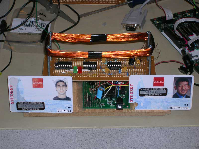
Figure 15: Our ID Cards Posing With the RFID Reader
All in all, we consider this project to be a success. While we were not able to discern the method to translate ones actual Cornell ID number into an RFID tag, we were still able to wirelessly extract the code and process it for meaningful use. It was a particularly rewarding experience; especially since we had a large amount of uncertainty going into the project; mostly due to the fact that we were dealing with cards which were manufactured to largely unknown specifications. Through much research and testing, we were able to develop a system which not only met our preliminary goals, but even met some of our more ambitious goals, such as remote administration for adding codes to the code database.
Through many of the stages of our design, there were two websites in particular which provided the neccessary information for us to figure out the best way to proceed. These were the Microchip® microID 125 KHz Reference Guide (especially their 125 KHz reader reference design), and Jonathan Westhues's website about Prox cards. In fact, brief email correspondance with him led us to finding the 125 KHz Reference Guide!
This project was mostly a test of what we could acheive utilizing as many resources as we could from Atmel. However, for this were to be a truly useful system in the real world, most of the code keeping/checking would have to be moved offboard onto the administrator computer, which has infinitely more computing power and memory. While our current design could certainly be used in the arena of which it was conceived (with a more protective housing and an actual locking mechanism instead of LED's, of course) we found that at the very least, we would have to get an Atmel MCU with more memory than the Mega32. As a proof of concept this works extremely well, but in practice a little more is needed. Another interesting tweak to the current design, could be the addition of a wireless transmittion interface to the adminstrative computer, allowing the reader to acheive more spacial independance from the base.
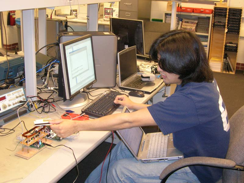
Figure 16: Ricardo Testing out the System and Doing Some Serious MultiTasking. We Don't Mess Around.
Appendix A: Budget Considerations
Most of our design was comprised of small IC's and discrete components. Thus we were easily able to stay within our $50 budget. A complete listing is below. For links to the neccessary data-sheets please click the links on the respective component.
Component Price Mega32 $8.00 Max233CPP+RS232 $8.00 Mega32 Protoboard $5.00 Soldier Board $2.50 CD4017 Decade Counter $0.39 74HC74 Hex Inverter $0.30 LM78M12Ct 12V Voltage Regulator $1.72 MM74HC04N D Flip-Flop $0.54 TL084 Quad Op-Amp $0.76 78F102J RF Choke $0.30 2N3906 PNP Transistor (2x) $1.72 2N3904 NPN Transistor $0.86 Misc Discrete Components (wire, resistors, capacitors) ~$10 Power Supply $5.00 Reader Housing (wood platform and 3" screws) $2.00 Total $47.09
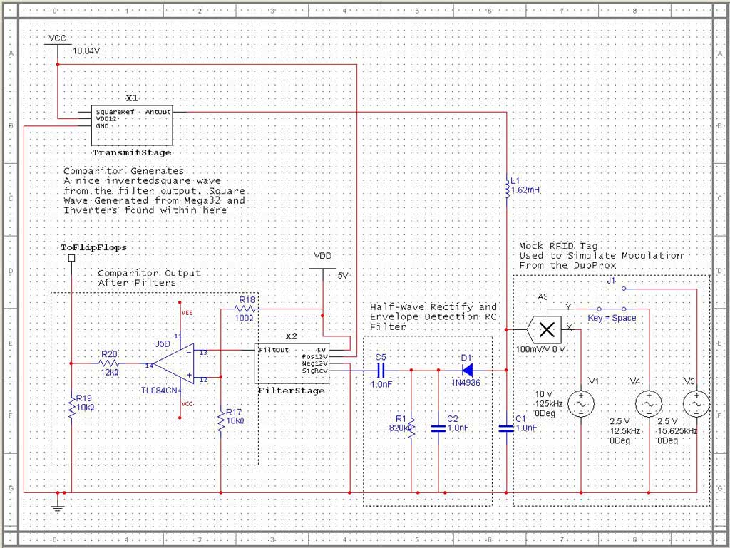
Appendix B: Final Circuit Schematic
Appendix C: Commented Code Listing
Appendix D: Citations and References
Jonathan Westhues's Proximity Website
microID 125 kHz RFID System Design Guide
FCC Rules
IEEE Code of Ethics
Wireless Retrieval of a Mouse's Vital Signs via RFID
Minimum Mass Wireless Coupler
Craig Ross
Simulation of hardware in Multisim
Soldering Protoboard
Constructing and soldering transmit stage
Code for different modes of reader operation and admin interface
Website CompilationRicardo Goto
Constructing and soldering Half-Wave Rectifier
Constructing and soldering flip-flop/counter circuit
Devising an algorithm to interpret the 540 bit response
Code for sampling the data and decodingBoth
RFID research
Soldering the filter stage
Determined the encoding scheme of the Cornell ID
Writing for website
