Our final project is the CUSat Diagnostic Board (CUDB). This board will be used for monitoring CUSat system health as well as performing various functions allowing for easy integration and debugging of CUSat components.
CUSat is the Cornell satellite team's entry into the Nanosat-4 competition sponsored by the Air Force Research Labs (AFRL). A significant milestone for CUSat is entering the "flat-sat" stage of manufacturing. This is where all satellite components are electrically connected on a clean-room bench, but not structurally integrated into the satellite frame. To make flat-sat debugging and integration easier, we have developed the idea of the CUSat Diagnostic Board (CUDB).
This project involves the combination of many circuit systems and many software systems. We have split up the report into several sections. Sections 3 and 4 of this report contain only design details. They do not contain the results of our tests and experiments to verify the functionality of the CUDB. Section 5 details our results of testing the various systems. Section 6 contains our conclusions.
The CUDB has the following functionality (each one of these functions is discussed in detail later in this report):
The design of the CUDB is such that we can "make life easier" for the other subsystems as they begin integrating their hardware into flat-sat. For example, the first subsystem to have hardware in flat-sat is the Power subsytem. The Power subsystem harnesses energy from solar cells, which will not operate while we are in lab. As such, the CUDB provides the 18.5 volts that the Power subsystem expects from the solar cells - letting the Power team test their hardware. Further, the Power subsystem has a battery charging circuit which CUDB can power. And, CUDB provides a method of discharging the batteries (normally done by running actual CUSat hardware in flat-sat).
For the reasons outlined above, the only way for CUSat to complete a finished product with the project's strict schedule is to have the CUDB operational by the time flat-sat is fully developed.
Most of the part selection has been completed by CUSat members Kris Young and Michael Austin. The basic PCB design was finalized by CUSat member Tyler Orchowski, and reviewed by Eric Brumer & Jiangang Shi. Our project entails:
Since CUSat is being developed for the AFRL, all components (including support equipment such as the CUDB) must comply with select military specifications (MIL-SPECs). Here are some specifications which must be followed for CUDB development:
A complete list of the military and department of defense specifications is not available to be published due to International Trade and Arms Regulations (ITAR) restrictions. However, if the reader is interested in mil-specs, please contact Eric Brumer for more information.
We would like to petition that we lift the cost constraint, as the CUDB shall be used for a Cornell project team.
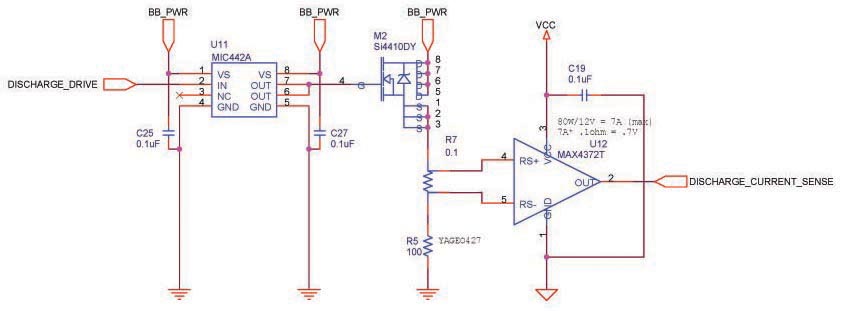
It is required that all power lines be monitored (current and voltage) in CUSat at all times. This is for the safety of all components on the satellite, and for the safety of the CUSat members working on flat-sat. Current sensing will be accomplished with the MAX4372T sense amplifier with a FET driver chip (MIC442A) and a FET switch (Si4410DY), as depicted in the following battery discharge circuit:
There are three power lines that must be monitored. The first is to measure the current draw while discharging the batteries. This is useful in calculating the battery capacity, as well as to ensure the batteries are discharging properly. If the batteries discharge too quickly, they may heat up and exceed the CUSat lab safety battery temperatures:
| Parameter | Limit |
| Maximum Battery Temperature | 50 �C for discharge, 40 �C for charge |
| Minimum Battery Temperature | 0 �C for discharge, 5 �C for charge |
| Maximum Array Voltage | 20V |
Taken from CUSAT-DD-00025-PWR-BATTERY-CHARGING-DESIGN written by Robert Zimmerman.
The battery discharge circuit (shown above) works as follows. PORT C2 on the MCU (labeled DISCHARGE_DRIVE) is input to a MIC442A driver chip. The FET driver chip is used for one main reason:
The output of the MIC442A is fed into a FET switch (Si4410DY), which controls whether or not the batteries (at VBATT = 12V) are discharged through a 100 ohm power resistor (labeled R5 in the above diagram).
If the Si4410DY is closed, the discharge current passes through a 0.1 ohm resistor (labeled R7) which is used for current sensing. The current sensing input is fed into a MAX4372T (current sense amplifier with a gain of 20). The maximum draw the CUSat batteries can produce is 7A (=80W max / 12V bus), which is well above any currents which will be seen by the 0.1 ohm or 100 ohm resistor. With a 12V bus, the total current drop through 100.1 ohms of resistance is 120mA, which is the expected current to be measured by the MCU.
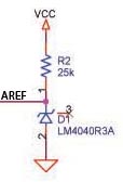
Since the output of the MAX4372T is fed into PORTF on the MCU, it is worthwhile to mention how we interpret ADC readings for current sensing at this time. The AREF pin on the MCU is set to a very stable 4.1V (circuit described later). Thus, if the ADC reading read 4.1V as the output of the MAX4372, that corresponds to a voltage drop of 4.1 / 20 = 0.205V across the 0.1 ohm resistor. This corresponds to a current of I = V / R = 2.05A. And, if the voltage read by the ADC was 0V, this corresponds to a current passing through the 0.1 ohm resistor of 0A.
Since we use the top 8 bits of the ADC as a measure of the current passing through the 0.1 ohm resistor, a read value of 255 corresponds to a discharge current of 2.05A, and a read value of 0 corresponds to a current of 0A. Therefore, to get the discharge current we simply multiply the read value by 2.05/255 = 0.008.
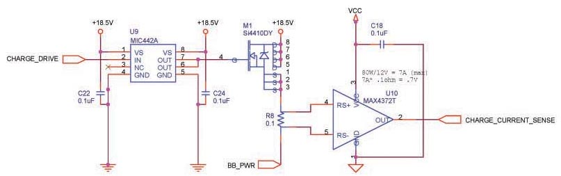
The second current sensor is used for measuring current while charging the batteries. PORT C0 of the MCU is input to a FET driver chip and a FET switch exactly as before. Here, however, when the FET switch is activated, +18.5V from the power supply is supplied to the batteries to charge them. The current entering the batteries is measured and sent to the MCU ADC. The following circuit shows the setup:
The last current sensor is used for measuring current supplied to the satellite power bus, and employs the same circuitry as described above.
All of our ADC measurements are with respect to an external AREF. We use an LM4040 4.1 (voltage shunt/zener diode) to provide a very stable 4.1V AREF. The circuit used is as follows:
Battery charging and discharging is done in conjunction with two of the three current sensing circuits (charge and discharge), and the CUSat power subsystem components. The CUSat power board (as well as the batteries being used) will not be discussed in this report, but it employs two algorithms (run on a separate microcontroller) to determine when the batteries have finished charging or discharging. For the CUDB alone, this will be done through manual inspection of the CUDB outputs using a multimeter. The battery voltage is run to the MCU through a connector to the batteries, labeled VBAT_SENSE in the schematic.
Battery charging is a complicated task in of its own, and we do not present the details of how CUSat performs charging and discharging. However, if CHARGE_DRIVE is asserted by the CUDB MCU, then 18.5V is supplied to the power subsystem. For testing purposes, we verify this using a multimeter. If DISCHARGE_DRIVE is asserted by the CUDB MCU, then a power supply (simulating the batteries) will source current through the 100 ohm resistor described earlier. This way, we can test the full functionality of the ADCs before we integrate the CUDB with the CUSat Power subsystem.
The CUSat data bus employs RS-485 serial communication. This is differential, bus based serial communications, where the difference on two wires is used to indicate logic 1 or logic 0. If the difference between the two RS-485 wires is greater than 200mV, it is logic 1. And if the difference between the wires is less than -200mV, it is a logic 0. We use the MAX3083 driver chip to turn the MCU's UART0 port to RS-485 compatible levels with the following circuit:
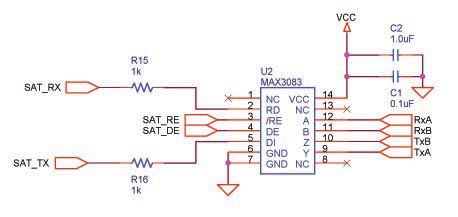
Here, SAT_RX and SAT_TX are TTL outputs of the CUDB MCU, which get converted to RxA, RxB (two differential receive lines), and TxA and TxB (two differential transmit lines). The two capacitors are bypass capacitors for the driver chip.
The two 1k resistors (R15 and R16) are to allow for microcontroller reprogramming. Section 4 of Atmel Application Note AVR042 states that in order to reprogram an Atmel MCU using SPI we cannot drive ports E0 and E1. However, in our circuit, we are driving those pins; we connect E0 and E1 to the MAX3083 driver chip (E0 = SAT_RX, E1 = SAT_RX) as UART0. In order to allow for reprogramming, the application note suggests inserting 1k resistors between E0 and E1 their corresponding driving inputs. This is a serious issue, and it is unfortunate that Atmel has this information tucked away in an application note instead of in the Mega128 documentation.
Note that SAT_RE and SAT_DE are the receive and transmit enable (respectively) of the RS485 driver chip, and are MCU controlled (SAT_RE = PORT C5, SAT_DE = PORT C6).
The CUDB must communicate with RS-232 on a PC: we use the MAX3322 driver chip to turn the MCU's UART1 port to RS-232 compatible levels. The circuit used is in the following diagram:
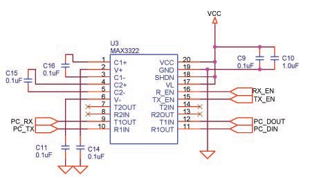
RX_EN and TX_EN are MCU controlled lines (PORT C3 and C4 respectively), and PC_DOUT and PC_DIN are hooked up to PORT D3 and D2 (UART1). PC_RX and PC_TX are the RS-232 levels which connect to the PC's serial port.
One of the requirements for all satellites to be launched into space via an Air Force launch vehicle is that solenoid-based electromechanical safety inhibits be in place between all power supplies (batteries & solar cells) and their loads (subsystems). This is to ensure (mechanically) that the batteries do not supply power to the rest of the satellite before the satellite has been ejected from the launch vehicle (ie: the satellite doesn't turn on while it is being launched into space).
The inhibits which will be in place on CUSat require +/- 12V to operate. The CUDB will provide this voltage through a series of switches and regulators and software controlled. The final inhibit signal is labeled INHIBIT.
The following schematic contains our implementation of the INHIBIT generation scheme. PORT G0 (INHIBIT_DRIVE_POS) from the MCU is connected to a FET driver / FET switch like in the current sensing circuitry. PORT G1 (INHIBIT_DRIVE_NEG) from the MCU has a similar setup.
G0 is the positive inhibit driver: if it is asserted, then INHIBIT is connected to the CUDB power source (a power supply for the CUDB, but it will be the solar cell array and batteries on the complete CUSat). If G1 is asserted, then the +12V power source is brought to a TI-059 regulator which transforms this +12V signal to a -12V signal, then fed to the INHIBIT line.
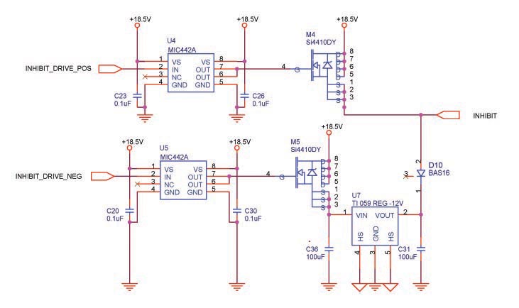
If G1 and G0 are both asserted at the same time, then 12V from the power supply will be connected to the output of a -12V driver (which has low output-impedance). This condition is extremely hazardous, and must be avoided. The current design of CUDB has this accomplished in software: the code must ensure that G0 and G1 shall never both be asserted at the same time.
Please note that although the schematics show the power source as +18.5V, this is just a label for the output of the special-purpose connector we are having donated to us. The CUSat diagnostic board's next revision will include this connector (which has a wall-power adapter) and a digital potentiometer which can control the trim of the regulator on the connector. This way, we will be able to very accurately scale the input power supply into the CUDB anywhere from 18.5V to 9V. The current version of the diagnostic board uses a +12V power supply.
Next revisions of the CUDB shall most likely include digital logic to control the inhibits, in the following fashion. The problem here is that it may be possible (during a digital transition) that 12V be connected to -12V.
| G0 | G1 | DRIVE_POS | DRIVE_NEG | INHIBIT |
| 0 | 0 | 0 | 0 | Floating |
| 0 | 1 | 0 | 1 | +12V |
| 1 | 0 | 1 | 0 | -12V |
| 1 | 1 | 0 | 0 | Floating |
Thus, DRIVE_POS = G0 & !G1, and DRIVE_NEG = !G0 & G1
Also, a diode is in place allowing current to only flow towards Vout of the regulator if INHIBIT_DRIVE_NEG is asserted.
Various bypass capacitors are used throughout the diagnostic board. For most components, a 0.1uF capacitor is placed in parallel with a 1uF capacitor. This is because we have several components which cause different levels of noise, and both capacitors are necessary for the correct operation of the system.
For example, without the 1uF capacitor from Vcc to Gnd on the RS-485 driver chip, there are 700mV noise spikes! That is enough to cause RS-485 communication to fail entirely. This noise is due to charge pump capacitors internal to the RS-485 driver chip which produces the proper differential voltage levels for RS-485.
As another example, the MIC442A FET driver manual strongly suggests the use of 0.1uF bypass capacitors to provide a clean driver output. So, all of the MIC442A's have 0.1uF capacitors from Vcc to Gnd physically close to the MIC442A.Also, the 16MHz crystal product manual suggests that 22pF capacitors be employed to reduce noise from the crystal.
Further, we employ two large Tantalum 100uF capacitors for use with the TI-059 regulator as charge pumps and bypass capacitors to generate a -12V signal.
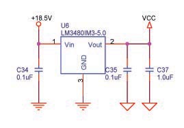
The main supply for power on the CUDB is supplied by an LM3480 voltage regulator using the following circuit. Again, please note that the current version of the CUDB has a 12V instead of 18.5V. The LM3480 can handle both inputs, so this component need not be different for future designs.
The current design calls for circuit breakers to act as extra safety for CUSat in the case of short circuits. These will not be implemented in the first revision of the CUDB, and are not a part of this project. They are, however, in the schematic.
LEDs are placed at various points in the CUDB to give diagnostic information about the current status of various systems. These systems include:
The following diagram shows the pinout of the MCU used on the CUDB. A list of all the pins follows, along with a short description of what the pin does.

| MCU Pin | Schematic Label | Purpose |
| PE0 | SAT_TX | CUCP Tx (UART0) |
| PE1 | SAT_RX | CUCP Rx (UART0) |
| PE4-PE7 | - | LED Drivers |
| PB1-PB6 | - | Used to control the digital potentiometer (in CUDB rev 2) |
| /RESET | RST | Used for on-chip reprogramming of CUDB. |
| XTAL1-2 | - | 16 MHz Clock |
| PD0 - PD1 | - | Used to control the digital potentiometer (in CUDB rev) |
| PD2 | PC_DIN | PC Rx (UART1) |
| PD3 | PC_DOUT | PC Tx (UART1) |
| PG0 | INHIBIT_DRIVE_POS | Drives INHIBIT to +12V |
| PG1 | INHIBIT_DRIVE_NEG | Drives INHIBIT to -12V |
| PC0 | CHARGE_DRIVE | Enables battery charging |
| PC1 | VBUS_DRIVE | If set high, CUSat is supplied with 12V bus power from the CUDB. |
| PC2 | DISCHARGE_DRIVE | Enables battery discharging |
| PC3 | TX_EN | PC Tx Enable (UART1) |
| PC4 | RX_EN | PC Rx Enable (UART1) |
| PC5 | SAT_RE | CUCP Rx Enable (UART0) |
| PC6 | SAT_DE | CUCP Tx Enable (UART0) |
| PF0-PF3 | BATT_THERM | Unused in current version |
| PF4 | VBUS_CURRENT_SENSE | ADC input: CUSat power bus current |
| PF5 | DISCHARGE_CURRENT_SENSE | ADC input: battery discharge current |
| PF6 | CHARGE_CURRENT_SENSE | ADC input: battery charge current |
| PF7 | VBAT_SENSE | Unused in current version. |
The microcontrollers in CUSat (in the Quad Flat Pack package) are soldered onto various printed circuit boards. And, all electrical components on CUSat exist within electronics boxes (Faraday cages). It is unacceptable (given the restricted CUSat timeline) that microcontrollers be taken out of their PCBs and electronics boxes to be reprogrammed. Thus, every microcontroller in CUSat shall have the ability to accept new code and reprogram itself.
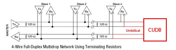
The new code will be transmitted over the CUSat network bus (serial RS-485) using the CUSat Communication Protocol (CUCP). The basic setup for CUCP is that there is only one bus master (the flight computer), and many bus slaves, hooked up in the following configuration. In the image, the black item represent current CUSat systems and are physically in the satellite structure, and are to be launched into space. The red items are called Electrical Ground Support Equipment (EGSE), and are only used for satellite integration and testing while on the ground. These components do not get launched into space. The Umbilical is a large set of wires and two large connectors which connect to all global data and power lines in CUSat. For example, the RS-485 data bus is part of the umbilical, along with various power lines, and extra wires with which we can reprogram the flight computer.
Note that there are NO dedicated lines with which we can reprogram microcontrollers. This is simply not feasible: We have 8 microcontrollers on the satellite, which would require an extra 16 lines to be placed on the umbilical. We cannot afford to route this many lines in the satellite. Microcontroller reprogramming is done through the current RS-485 data bus already designed and tested as a CUSat system component.
CUCP (in normal operations with one master) works as follows (actions by the master are in blue, and actions by the slaves are in black):
For microcontroller reprogramming, CUDB acts as the bus master, and we hijack CUCP halfway through the protocol to execute our own communication steps. Here, actions by the CUDB are in red.
This process is more complicated than it first appears, and is outlined extensively in the software design portion of this report.
It is important to remember that CUCP was designed with the intention of having one single bus master (the flight computer). Therefore, there are issues that must be dealt with to integrate a second bus master into the RS-485 network bus. The way to isolate the two masters is for the CUDB to disable the flight computer's RS-485 transmitter. This way, when the CUDB wants to transmit on the data bus, it first disables the flight computer's Tx abilities. Then it is safe for the CUDB to transmit. When it has finished, it can simply re-enable the flight computer's transmiter. This line (the flight computer driver enable line) will be routed through the umbilical to the CUDB.
The CUDB constantly collects data from power lines and snoops traffic on the CUSat network bus. This data is transferred in real-time to a lab PC running a custom made application (written for the ECE 476 project). This application also presents the end user with the ability to reprogram a selected microcontroller with code produced by CodeVision AVR. Also, the current battery capacity is updated in real time, and the application provides controls to charge and discharge the batteries.
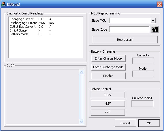
The application interfaces with the CUDB with a serial RS-232 9600 baud connection. It has a windows GUI interface, with the outline defined in the following graphic:
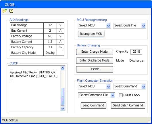
The GUI software is written in Visual C++ and is a windows executable. The end user has the following abilities:
The nature of the GUI to MCU communication is that the GUI will always initiate requests for data (or issue commands) before the MCU will respond. Every 100ms, the GUI will request the most up-to-date sensor readings from the MCU. The control flow for issuing commands is as follows:
The GUI code is very straightforward when viewing it in Microsoft Visual Studio, however it can be difficult to read on paper. A full copy of the code will be available on the website for this project, and if the reader is interested in viewing the whole GUI code in its glory, please open that project file in Visual Studio. The code performs the operations above, and it uses the Windows MFC (Microsoft Foundation Classes) as a toolkit to create all of the buttons and graphics seen in the GUI. A listing of the functional code (not including GUI creation) is available in the appendix of this report.
The code contains a serial port implementation taken for free from the internet (source unknown, as many copies of this are available without reference). The code is built into two threds of execution:
Some signal filtering is performed on the ADC readings by the GUI. We found that without any filtering, the displayed values for say, the discharge current, had 10mA fluctuations in its readings. To minimize these fluctuations, we attempted to perform a filtering technique where we only increase the displayed ADC value if the current value is greater than 10mA greater than the previously output value. And, we would only decrease the displayed ADC value if the current value is greater than 10mA below the previously displayed value. This did not work out as well as we though, so we resort to using a 5-history moving average filter. This provides very smooth-looking ADC values which are acceptable for human viewing in real time.
Since the CUDB must communicate with two systems using serial communication (the CUSat data bus using one protocol, and the PC running the GUI using another protocol), we opted to keep the CUDB code as simple as possible. All communication is interrupt driven, and all commands will be initiated by the GUI.
For example, if the GUI wants the latest ADC readings which have been sampled by the CUDB, then it requests them. Only when the GUI requests the information will it sent by the CUDB.
As another example, the CUDB constantly snoops bus traffic on UART0. This data is buffered internally. The GUI will request this information, and the buffer is emptied to the GUI and is displayed for the user to read.
To achieve real-time data updates for the user to see, the GUI requests the following from the CUDB:
We setup UART0 and UART1 to 9600 baud for snooping the CUSat data bus, and communication with the PC using:
    UBRR0L = 51; //9600 bps to MCU
    UBRR1L = 51; //9600 bps to PC
    UCSR0B = 0b10010000; //enable USART0 receiver
    UCSR1B = 0b10011000; //enable USART1 transmitter and receriver
We also initialize the ADC and use the timer0 compare interrupt to read the ADC every 50ms.
    // setup timer 0 compare to interrupt every 1ms
    TIMSK=2;           //turn on timer 0 cmp match ISR
    OCR0 = 250;        //set the compare re to 250 time ticks
                       //prescalar to 64 and turn on clear-on-match
    TCCR0=0b00001011;

    // setup ADC's
    ADMUX = 0b00100000;  //b76 =00, select AREF, internal Vref turned off
    ADCSRA = 0b11000111; //ADC enabled, start conversion, prescaler-128
The MCU has the following status variables, listed in the C-struct called ALL_MCU_DATA, and the global array called cucp_buffer:
    struct ALL_MCU_DATA {
        char CHARGE_CURRENT_SENSE;
        char DISCHARGE_CURRENT_SENSE;
        char VBUS_CURRENT_SENSE;
        char inhibitState;
        char batteryState;
    } allMCUData;

    unsigned char cucp_buffer[256];
| Variable | Description |
| CHARGE_CURRENT_SENSE | ADC output of battery charging circuit. To obtain the measurement of the current entering the batteries to charge them, multiply this number by 0.008. |
| DISCHARGE_CURRENT_SENSE | ADC output of battery discharging circuit. To obtain the measurement of the discharge current, multiply this number by 0.008. |
| VBUS_CURRENT_SENSE | ADC output of bus power circuit. To obtain the measurement of how much current is being supplied to the CUSat power bus, multiply this number by 0.008. |
| inhibitState | Current state of the inhibit circuitry.
A value of 0xA indicates that the inhibits are in the +12 state. A value of 0xB indicates that the inhibits are in the -12 state. A value of 0xC indicates that the inhibits are off. |
| batteryState | Current state of the battery charging circuitry.
A value of 0x7 indicates that the batteries are charging. A value of 0x8 indicates that the batteries are discharging. A value of 0x9 indicates that the batteries are not being charged or discharged. |
| cucp_buffer | Buffer containing snooped CUCP traffic. This buffer is 256 bytes long, and wraps around if more than 256 bytes of CUCP
data is snooped before the GUI requests the CUCP data. This limitation is not a serious issue, for two reasons:
|
The GUI always sends commands to the CUDB in order to both change the CUDB's status and to request information which the CUDB has stored. When the GUI sends one byte of command to the CUDB, the CUDB responds with an echo of this byte for verification purposes. Here is a list of the commands and their actions:
| Command | Value | Description |
| DB_CMD_REPROG_MCU | 0x01 | GUI is commanding the CUDB to reprogram a microcontroller (full description of command operations in section 4.3.5) |
| DB_CMD_GET_ALL_DATA | 0x02 | GUI is requesting all the ADC readings and the current CUDB status variables (described in section 4.3.3) |
| DB_CMD_GET_CUCP | 0x03 | GUI is requesting all the CUCP snooped responses (described in section 4.3.3). Here, the CUDB first sends how many bytes have been snooped, followed by the bytes themselves. |
| DB_CMD_BAT_DISCHRG | 0x04 | GUI is commanding the CUDB to discharge the batteries |
| DB_CMD_BAT_CHARGE | 0x05 | GUI is commanding the CUDB to charge the batteries |
| DB_CMD_BAT_OFF | 0x06 | GUI is commanding the CUDB to disable battery charging/discharging circuits |
| DB_CMD_INHIBIT_POS | 0x07 | GUI is commanding the CUDB to enable the +12 inhibit line |
| DB_CMD_INHIBIT_NEG | 0x08 | GUI is commanding the CUDB to enable the -12 inhibit line |
| DB_CMD_INHIBIT_OFF | 0x09 | GUI is commanding the CUDB to disable all inhibit lines |
The CUDB makes use of hardware timers to perform ADC readings. Every 100ms, the get_adc_data() function is called, which reads the current ADC readings (all of the MUX channels being read, as described in the previous sections of this report) and sets the ADC to take another reading. When the ADC data is read, we simply store the top 8 bits in the appropriate global variable within the ALL_MCU_DATA struct, overwriting the previous value. This way, when the GUI requests the ADC data, all the CUDB must do it send the current value inside the appropriate variable in the ALL_MCU_DATA struct.
Serial communication is entirely handled through interrupts. The UART1 interrupt is for communicating with the GUI. Whenever the GUI sends the CUDB a command, UART1 will first echo back the command, and then set the global CUDB command variable (called db_cmd) to a value depending on the incoming command. Then, when the while(1) loop in the main function sees a change in db_cmd, it acts appropriately. After acting (by calling the appropriate function which performs the CUDB functions, it sets db_cmd back to NO_ACTION, indicating that the action has been handled.
To prevent the user from entering information into the GUI too quickly (and thus possibly causing problems with two commands being read by the CUDB before the first command is acted on), the GUI waits 100 milliseconds before allowing the user to enter another command.
If the user wishes to reprogram a microcontroller, more steps must be included. This is where the global status variable (called status) comes into play. The status variable transitions as the CUDB progresses through the reprogramming steps. When the GUI commands the CUDB to reprogram a microcontroller, the CUDB enters the REPROG_MCU_GET_ADDR state. The GUI then relays all incoming information from the GUI to the subsystem to be reprogrammed, and it relays all incoming information from the subsystem to be reprogrammed to the GUI. This way, the CUDB acts as a forwarding device.
However, this is not as simple as it seems. The bootloader code does not operate with the same UART settings as the normal CUCP code. The version of CUCP to fly on the satellite will be 230kbit, using 9 bit words. However, the bootloader runs at 9600bps, with 8 bit words. This is done because of the possibility of clock skew in UART transmission. At 230kbit with a 16MHz clock, the UART on the Mega128 has a baud-rate error rate of 8% (meaning that its clock differs from true 230kbit/s transmission is off by 8%). However, for 9600 baud, the error rate is 0.2%. Since we are transmitting sensitive information over the bus (microcontroller code) we do not want to risk any skew errors in transmission (as it may corrupt the subsystem, and therefore all of CUSat), so we opt for a slower baud rate. During normal satellite operations, more care is taken to detect these transmission errors (all done on the flight computer), but we can not perform the same functions on the ground using a microcontroller - we require a more powerful processor.
Thus, when the subsystem to be reprogrammed enters the bootloader code, the CUDB must change its UART settings. Further, before sending any information out on the RS-485 bus, the CUDB must disable the flight computer's transmitter, and enable its own. Then, once the reprogram is successful, it disables its own transmitter and then enables the flight computer's.
The bootloader code must perform the following functions:
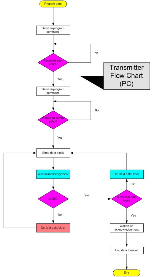
Most of the above points are satisfied with the following flow control (PC and CUDB-side). To make this explanation simpler, we assume that the CUDB performs without faults and can relay all messages from the GUI to the subsystem (and vice versa).
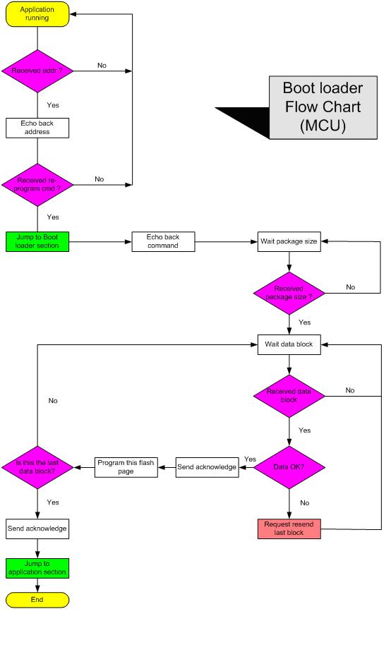
The following diagram shows the state flow for the microcontroller to be reprogrammed. We begin in the CUCP state, receive (and echo) our address, receive the command to reprogram, and then we jump to the bootloader code. We use Codevision AVR to program the MCU initially to place the bootloader code (with a maximum size of 1kB) beginning in flash location 0xFB00. Thus, jumping to the bootloader code is a simple jmp 0xFB00 assembly instruction.
Once we are in the booatloader, we echo our address. Then the GUI sends the number of packets in the code file. Each packet is precisely the size of a flash page, which is 256 bytes. This is followed by a 2-byte CRC, which we must verify. Once we have verified this, we write the flash page to memory, beginning at location 0x0000. We perform this for each packet. Once we have received, verified and written all flash pages, we send a "reprogramming complete" byte to signal the completion, and we reboot.
Writing 256 bytes of data to flash is accomplished by running through the following procedure:
    void boot_page_ew(unsigned long p_address, char code) { // erase(code=0x03) and write(code=0x05)
        #asm
          ldd r26,y+3                    ; Byte 2 of address
          out 0x3b,r26                   ; RAMPZ-Bit0
          ldd r30,y+1                    ; Z register low byte (byte 0 of address)
          ldd r31,y+2                    ; Z register high byte (byte 1 of address)
          ld  r22, y                     ; Get the code (2nd arg)
          sts 0x68, r22                  ; Set spm instruction to erase flash page
          spm                            ; Executes flash erase
        #endasm
    }
    void wait_page_rw_ok(void) {
        while(SPMCSR & 0x40) {           ; Read-while-write status buffer = 1, page erase or page write in progress
            while(SPMCSR & 0x01);        ; Wait until flash operation complete
            SPMCSR = 0x11;               ; Set spm to re-enable read-while-write
            #asm("spm");                 ; Re-enable read-while-write
        }
    }
    void boot_page_fill(unsigned int address, int data) {   // write a word to temporary buffer page
         #asm
           ldd r30, y+2                  ; r30 = LSB of address
           ldd r31, y+3                  ; r31 = MSB of address, address in the Z-register(R31:R30)
           ld r0,   y                    ; LSB of data
           ldd r1,  y+1                  ; MSB of data
           ldi r22, 0x01                 ; r22 = 0x01
           sts 0x68, r22                 ; Set spm to write to temporary page
           spm                           ; Write r1:r0, byte # [r31:r30] of temporary page
         #endasm
    }
The above code must be called for every two bytes for the 256 byte packet.
Generating the code file which is sent to the microcontroller is not a trivial task. First, we must write the program using Codevision AVR. Then, compiling the code creates an output file called <project name>.HEX. This is the code in the .hex file format for AVR machine code. Each line of the .hex file has the following structure:
| Byte # | Description |
| 1 | Record Marker: The first character of the line is always a colon (ASCII 0x3A) to identify the line as an Intel HEX file |
| 2-3 | Record Length: This field contains the number of data bytes in the register represented as a 2-digit hexadecimal number. This is the total number of data bytes, not including the checksum byte nor the first 9 characters of the line. |
| 4-7 | Address: This field contains the address where the data should be loaded into the chip. This is a value from 0 to 65,535 represented as a 4-digit hexadecimal value. |
| 8-9 | Record Type: This field indicates the type of record for this line. The possible values are: 00=Register contains normal data. 01=End of File. 02=Extended address. |
| 10-... | Data Bytes: The following bytes are the actual data that will be burned into the EPROM. The data is represented as 2-digit hexadecimal values. |
| Last two | Checksum: The last two characters of the line are a checksum for the line. The checksum value is calculated by taking the two's complement of the sum of all the preceding data bytes, excluding the checksum byte itself and the colon at the beginning of the line. |
The .hex file format has extra information that does not belong in the MCU flash. Therefore, we run a free utility called HEX2BIN which transforms this .hex file into a .bin file, which contains only the code to be written to the microcontroller flash. Thus, we send the .bin file to the MCU.
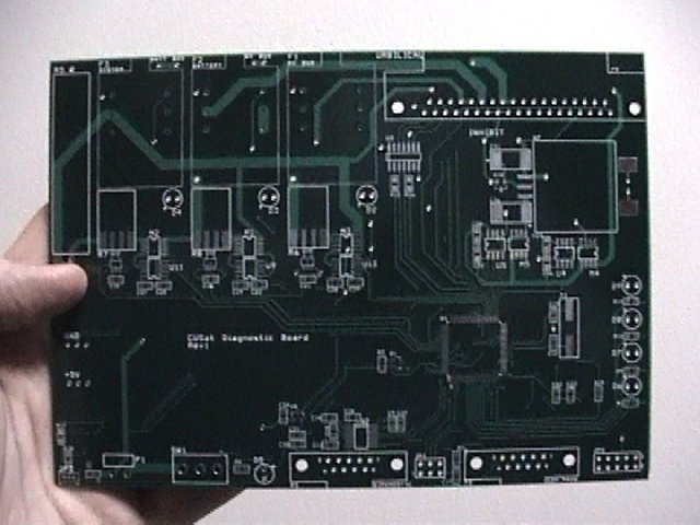
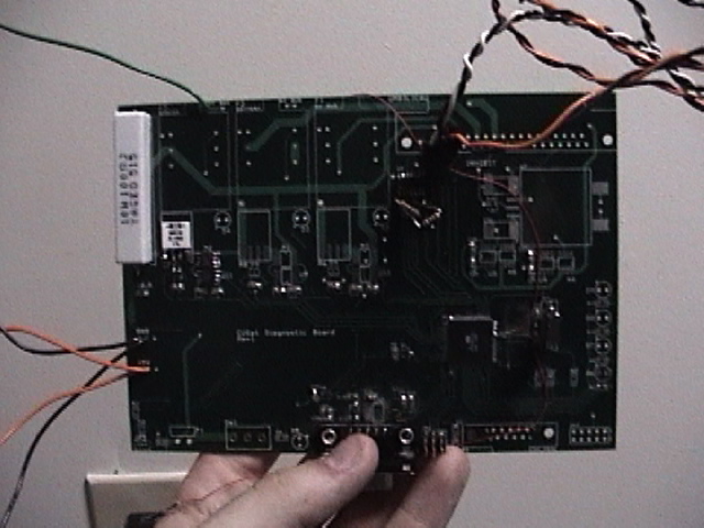
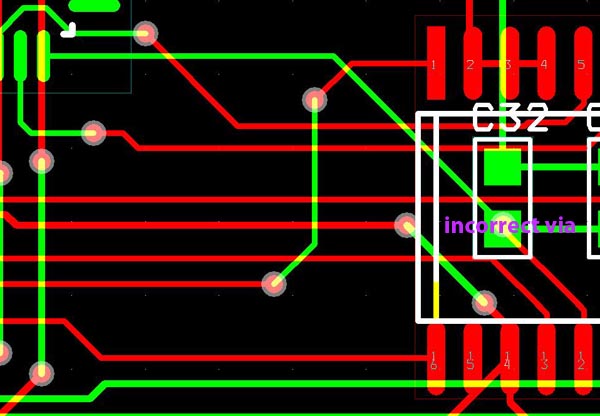
The following images show the unpopulated version of the board, and the final populated version of the CUDB revision 1. Note that only one of the three ADC circuits is populated. Further, the inhibit circuit (top right of the board) is not populated. And, some connectors are not placed (as we do not have the components in our posession yet). All of this will be explained thorughout section 5.
We found several bugs in the design, which will be fixed in the next version of the board:

When initially populating and testing the board, the first step for most PCB designs is to solder on all decoupling capacitors, solder on the main voltage regulator(s), verify some basic connectivity, and then test the circuit without any other components soldered down. It took less than one second and a small puff of smoke for us to realize that this is a best engineering practice for a reason.
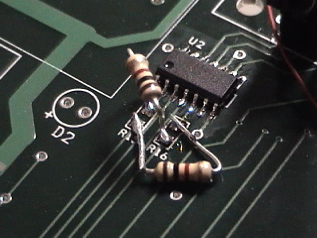
We blew our voltage regulator the first time we hooked up an 18.5V input voltage to it. Initially, we thought that the regulator may have been getting too hot because we were approaching its maximum input voltage. The spec sheet claims that the absolute maximum input voltage is 30V, and 18.5V is getting close to that. So, we soldered down another voltage regulator and set our input power supply down to 5V. This time, Eric placed his finger on the voltage regulator to see if it was overheating. One second later, we have another puff of smoke and a burnt finger.
It turns out that the voltage regulator had been hooked up backwards according to the layout! We were suppling 18.5V and 5V with unregulator current to the output of a 5V regulator! To fix this, we soldered down another regulator upside down (literally!). But, two fried chips and a burnt finger were not the only results of our power regulation woes. After examining the spec sheet more closely, we saw that the regulator could only source 100mA of current. We want to drive a Mega128 running at 16MHz, two serial communication drivers, numerous FET drivers and switches, as well as four debug LEDs off of a voltage regulator which could only source 100mA of current! This is a problem, and we must change our choice of regulator in the next revision of the CUDB. We will most likely use a PT78ST100 series regulator, which can source up to 1.5A of current. For the current design, we apply 5V from a power supply directly into a Vcc/Gnd pin jumper.
Due to the 'situation' with voltage regulators on the CUDB, we do not feel safe (literally) with putting the inhibit switching circuit on the current revision of the CUDB. If we missed an important point as a powerful enough voltage regulator, then we may have missed something else with the inhibit switching circuit (discussed in section 3.4). And, since the inhibits handle +/-12V we feel there may be danger to other components (and to us) on the CUDB. Further, since software problems could cause there to be a short between +12V and -12V, we felt the risk factor not acceptable to attempt the inhibit circuitry.
Our plan of attack for the inhibit switches is to breadboard the entire circuit and test it THOUROUGHLY before bringing the components anywhere near the other, functioning circuitry of the CUDB. We are unsure of things like possible electromagnetic interference which may cause problems with our serial communications, and the behavior of the system in the case of a short. More design work needs to take place, along with more safety work, before the inhibits are to be placed on the CUDB. We can also breadboard our digital logic circuits.
The only issue with having to test and breadboard more circuitry is that it may push back the delivery date of the completed diagnostic board. However, the safety of CUSat and the engineers working on it comes before schedules on the team.
Our original plan had been to test the battery charge and discharge circuit with the CUSat batteries. However, since our board was shipped to us so late, we did not have the opportunity to integrate our battery charging circuits with the CUSat power system. Thus, we opted to test the response of the ADCs, and how well the GUI was able to display real-time ADC information.
Our setup involved a power supply (simulating the batteries) being discharged through our discharging circuit. We tested all situations involving the GUI battery discharging and disable buttons, and changing the dial on the power supply to input a higher voltage. We tested the following situations:
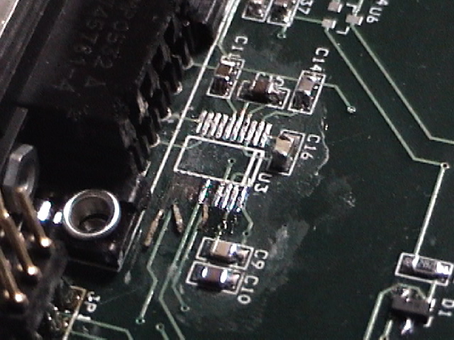
The trickiest part of the ADC circuits is soldering the various components onto a very tight space. The sense resistors (as shown in the following picture) have four leads and are very large. However, when the component is lying flat on the PCB, the leads do not make contact with the solder pads. Therefore, in order to solder the sense resistors on, you must actually place solder UNDERNEATH the component's leads. This proves to be very tricky, especially since the leads are fairly close together, and we do not want to damage other components which are close by (capacitors, the FET drivers, FET switches, etc).
By the stability of our readings, it appears that the LM4040 zener diode appears to give a stable AREF! We will continue to use this device in future versions of the board.
Since we did not have batteries with which to test our charging circuit, we felt there was no need to populate the rest of the ADC circuits. They are all use the same components as the discharge circuit, which operated correctly. Plus, since we do not have the proper voltage regulators, and we do not have batteries, it would simply be a waste of time since there is nothing more we could test than what has been tested already.
The GUI looks and feels very natural and comfortable. This is important in designing any GUI which will be used in a real-world system, as it lets the end user focus on their work, instead of having to deal with faulty or strange looking user interfaces. Also, since the GUI operates just like any other Windows-based program, there is very minimal learning time involved with the GUI. Pictures of the GUI can be found throughout this report.
Currently, there may be some issues with response-time and deadlock conditions, although they are not very apparent on the surface. As discussed before, the GUI executes a thread which polls the CUDB for ADC information and CUCP snooped data every 100 milliseconds. If the CUDB loses a packet of information, or if it stops responding (due to a serial port failure, a wire disconnect, etc), then the CUDB will hang silently. If the ADC thread is waiting for a response, then no other buttons are allowed to be pushed, and the program hangs. To fix this in the next revision of the GUI, we will place timeouts in strategic places and insert error notification that a timeout occurred. This way, the program will never hang, and the GUI operator need not be confused as to what is happening.
Also, there currently isn't any logging mechanism in the GUI. This may prove to be extremely useful in debugging CUSat in the case of an error. It is generally a best-practice in the spacecraft industry to keep extensive logs of all operations, whether it be to sign out a piece of equipment from a locked cabinet, keeping old versions of flight code, and even logging debugging data. In the next version of the GUI, we will add the automatic time stamping and logging of all ADC readings, all CUCP bus transactions, and all user button presses, such that we will be able to recreate the situation in the case of an error.
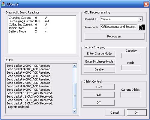
MCU reprogramming went off very well. The only issues we had were with the RS-485 driver having some cold solder joints, where the electrical contact was not perfect. After re-soldering the component on the PCB, microcontrollers were able to accept new code and reprogram themselves great! The following two pictures show what is displayed on the GUI when a microcontroller (in this case, the CAMERA microcontroller) is being reprogrammed with new code.
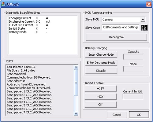
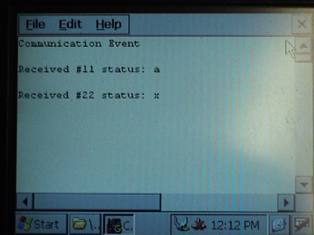
We do not have direct access to the internals of the CAMERA microcontroller. But, since it is already hooked up to the CUSat communication bus, we can use the flight computer to verify that new code has actually been accepted by the subsystem. The original code was the following:
    #define NET_ADDR NETWORK_ADDRESS_CAMERA
    #include "cucp.h"
    #include "CUCP Includes/cucp_def_cam.h"

    void main() {
        CUCP_Init();

        #asm("sei")

        CAMStatus.myStatus = 'x';

        while(1) {
            if (Net_Msg_Status == MSG_EBSRIE) { // Command and payload have been received
    	       Net_Msg_Status = MSG_READ;
    	       switch (Net_Cmd) {
    	           case NET_CMD_GET_STATUS:
    	               send((BYTE*)CAMStatus, sizeof(struct RESP_STATUS));
    	               break;
               }
            }
        }
    }
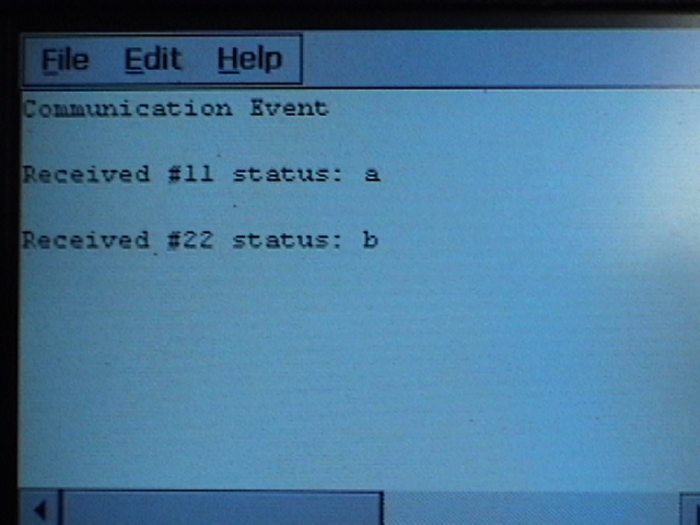
And the updated code had one change: we changed the CAMERA status to a different letter. The changed line is:
CAMStatus.myStatus = 'b';
Then, we used the flight computer and CUCP to receive the current status of the subsystems. We used this to show that the code was updated! See the following pictures for the output of the flight computer! Please note: there is no use in describing the CUCP interface, but it suffices to say that on the CUCP command NET_CMD_GET_STATUS, the CAMERA subsystem will transfer one character (it's status).
Generally speaking, interfacing one system with another is a tricky task. Each of the systems is fine-tuned to exist in its own right, and may not lend itself well to being adapted for use with another system. This section focuses on such integration issues and how we work around the various problems associated with the integration of systems.
Our first revision of the PCB was supposed to come in one week before we did our demo. Due to some confusion while ordering the boards, we ended up with a PCB in our hands on Friday morning. Here's a picture of a smiley Eric holding the board that we received, along with the layout of the CUDB.

It took us about 30 seconds before we realized the obvious: that isn't our board! There had been a shipping screwup which added an extra load of stress to already overworked Cornell ECE476 students! We sorted out the shipping fiasco, and obtained our board Saturday morning.
The moral of this section is to ALWAYS add in at least one week of leeway in ordering any components for any project with a deadline. For most CUSat components, we have added in margins to the manufacturing schedules and for part delivery times, etc. And this drives the point home even more.
Looking back at the work we've done, it looks like our software is more robust and thoroughly tested than our hardware. We attribute this to the amount of time that we had to work on the CUDB once we got the PCB in due to some shipping problems. Also, some part selection did not seem to be wise (namely, the voltage regulators). But this is precisely what revision 1 of a board is for! The next verion of the board will include:
Further, now that we have the ADC circuitry working, it is simple to replicate the circuits to measure any currents on any lines we would like! Also, we can then add in voltage sensing, to give us an accurate depiction of the power utilization of the satellite and its various components.
Now, we are able to progress to rev 2 of the CUDB. Wish us luck!
Article 1 of the IEEE Code of Ethics states that all safety issues be taken seriously in the development of any technology. This applies to the CUDB, mainly in our inhibit switching, and in our battery charging and discharging circuits.
The way our inhibits currently function contains with it a safety concern. It is possible that a glitch in software can cause a +12V to -12V short circuit. In testing the CUDB, this will result in a short in the power supply being used, and if the power supply is configured correctly, it will break its own internal fuses and cut off power to the CUDB. However, when the CUDB is used on CUSat, it may cause more serious problems with both the connector supplying the power, and damage to CUSat if the power leaks onto the CUSat power bus. We recognize this safety issue, and have explicit comments in our software documentation as not to cause the aforementioned situation.
Another factor for concern is battery charging and discharging. CUSat uses NiCd batteries, which pose a health threat if they are damaged (they may leak, or smoke). The CUDB has software inhibits to prevent too much current from entering the batteries, and the CUSat Power components (on the CUSat power board) contain electrical inhibits to prevent this. We feel that this double protection is adequate for our use, especially since all CUSat members are trained through the Engineering College safety training.
Honesty about system safety plays an important role in all aerospace systems and applications. All safety critical information MUST be supplied with all CUSat components to any engineers who wish to work on a specific component, such that no harm comes to the engineer or the components they are working on. For example, the CUSat thrusters produce an exhaust plume (of vaporized teflon), which may interfere with solar cell efficiency, and causes electromagnetic interference which may affect our GPS subsystem. This information is critical to the safety of the CUSat components: all CUSat Propulsion members are aware of the potential damage the thrusters can cause.
This directly applies to the CUDB, in that we can cause current spikes through switching inhibits on and off. These spikes may affect other subsystems, and a thorough analysis must be performed to ensure that if any problems arise, they are well documented. Further, we must be sure of the effects of the CUDB battery charging/discharging circuits when used in conjunction with the power susbsytem charging/discharging circuits. Could the batteries overheat if both the solar cells and the CUDB are charging them? Or, what happens if the batteries are powering some subsystems, and then the CUDB adds an extra load and begins discharging the batteries through the 100 ohm resistor. These situations must be taken seriously by members of the Integration & Testing team on CUSat, for the safety of the mission and of CUSat members.
Article 4 states that no bribes shall be accepted. And none were (-:
Jiangang developed all of the CUDB code to run. This entails setting up all the tasks, status, and commands mentioned in section 4.3. He also developed the MCU reprogramming code: from the output of Codevision to a new program running on a microcontroller.
Eric oversaw the PCB design, and populated the CUDB with discrete components. He also wrote the C++ code for the GUI, and wrote most of the report and webpage. Eric also (through his work in CUSat) developed the testbed which the CUDB is tested on.
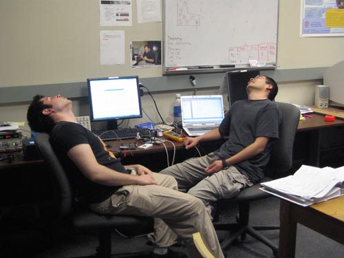
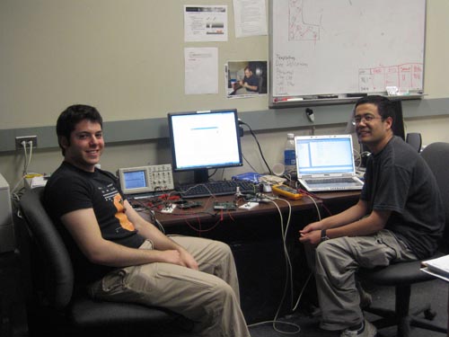
Both Jiangang and Eric tested and integrated the components with the CUSat test bed of flat-sat. Since we obtained our board the Saturday before our demo on Monday, we were in the CUSat lab nearly the entire weekend working on the CUDB and finding problems. We were certainly excited once we got it functional! Here is a picture of us immediately after we finished our work:
And here is a picture thirty seconds later