Machine de Karaoke by Song Du, Jae-Hoon Lee, Jae Young Cho and Sining Qi
Sound bite
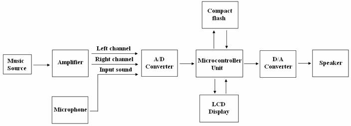
Our project is a karaoke recording machine which is capable of removing the voice component of a music file and storing the user��s singing voice with the background music to an external compact flash memory. It can also be used as a stand-alone voice recorder.
Summary
Our Karaoke machine has 6 modes. It also works as a digital voice recorder.
In the recorder mode, a musical file is read from an iPod. The vocal in the music can be removed. The remaining background music is added to the recorded sound signal acquired by a microphone. The playback sound therefore consists of the original music and the recorded sound. In order to have high quality sound, a relatively high recording speed is required, say 20KHz. An external serial mutli-channel ADC is used to extract the music signal. Considering the size of data, the local microcontroller memory does not have enough space to store such a big file, therefore an external storing device, like a memory flash card, must be used.
Motivation
The motivation of doing this project is to implement the ongoing research project under Professor Sergio Servetto��s group.
��
Rationale and sources of your project idea
The rationale of the Karaoke machine is mainly for entertainment. The design idea also came from a research project under Professor Sergio Servetto's group. By making some modifications we can increase the recording rate to be as high as megahertz.
Background
The method of removing vocal inside a song is to subtract the left channel from the right channel, or vise versa. This idea is based upon the fact that, during stereo recording, the singer is usually placed in the middle of the left and right microphone. Most instruments, however, are not. The result is that the singer's voice is the same in the right and left channel, while majority of the instrumental sounds are slightly different in two channels. By subtracting the left and right channel, the vocal will be removed and the music shall remain. This is by no means a perfect technique because the assumption about the singer might not be true in some cases. And due to the echoes, the vocals cannot be completely removed, some "ghostly" sound always remain in the background. In addition, typically the bass instruments, such as drum, are usually placed in the middle as well. By using the method described above, the bass component of the music would be reduced as well. One possible way to solve this issue is to attach a low-pass filter to one of the input and leave the other channel alone. Due to time constraints, we did not implement the filter.
Logical structure
Fig 1: system block diagram
Specifications:
Recording rate: 10kHz
Memory: 96MBytes
Recording time: 160 minute
Functions:
Mode 0: Playback a song without any modifications, no recording
Mode 1: Playback a song without vocal in it, no recording
Mode 2: Playback a song with vocal and singer's voice and record it into the external memory
Mode 3: Playback a song without vocal and record it into the external memory
Mode 4: Removing the vocal part of a song and storing the user��s singing voice with the background music to an external compact flash memory.
Mode 5: Recording user's voice into compact flash memory, no music
Mode 6: Direct reading from memory
Standards
To record sound onto an external memory device, the format of that specific device needs to be known. For this project a compact flash will be used. Therefore, the IEEE standard of the flash drive��s format needs to be investigated. In addition, the method to communicate between the microcontroller and the drive should follow certain protocols.
Patents, copyrights and trademarks
The original record labels hold the copyright to the music we have used. We are not using them for commercial purpose.
Karaoke Part
The hardware work involved in the Karaoke part mainly consists of two parts: ADC part and DAC part. The board layout is the shown as follows:
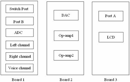
Fig2: Bread board layout
1. Music sources
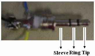
Fig3: Phone jack
The configurations of phone jack for microphone and speaker are as follows:
|
�� |
Microphone |
Stereo speaker |
|
Tip |
Single |
Left channel |
|
Ring |
Power |
Right channel |
|
Sleeve |
Ground |
Ground |
Table1: Phone jack configuration
Therefore three channels of signals, which are left channel, right channel and voice channel, are fed into a multi-channel ADC at the same time.
2. ADC -- MCP3204
MCP3204 is a ADC chip with 4 input channels and serial output which has 12 bit resolution. Given a 5V reference, the smallest detectable voltage change is 1.22 mV. The noise level in the circuit is already significantly higher than this value. However, other parts of the circuit limited the use of all 12 bits. Realistically, only the most significant 8 bits of the ADC output can be used. Since the analog output of Ipod and microphone are relatively low, in the 100mV range, some pre-amplifying circuitry needs to be constructed before A/D conversion. In addition, all the audio sources contain positive and negative amplitudes. In order to convert the negative amplitudes, a DC shift needs to be provided.
The circuit designed to
accomplish the aforementioned goals is a simple op-amp that utilize both the
inverting and non-inverting input end. The resulting output signal is generated
according to the following equation: ![]()
��
For left and right channels: R1=10kohm, R2=100kohm, Rx=50kohm, Ry=3khom, Gain=10
For voice channel: R1=2kohm, R2=10kohm, Rx=10kohm, Ry=10kohm, Gain=5
The resistor values are carefully selected so that the DC bias is 2.5 V and the peak-to-peak value of Vout is around 4V. 4V is selected here because occasional high amplitudes in the original input might cause the output to clip if the gain is too large. A relatively small gain could reduce the occurrence of such event.
During the testing process of the ADC circuitry, three ADC chips stopped working after a few rounds of initial testing. This caused great frustration because to continue the work, a new ADC needs to be purchased and shipped by the vendor. One possible cause for this could be that the original amplifying circuitry used ��5V power supply. Although the output of the amplifier is calculated to be within 1V to 4V, it could go below zero and cause damage to the ADC chip. A more critical mistake was that the analog ground and digital ground pin of the ADC are connected to grounds of two separate systems. After connecting those two grounds, the ADC chip did not fail again. The noise level also dropped dramatically.
To reduce the noise in the circuit, by-pass capacitors are used between power and ground for each chip.
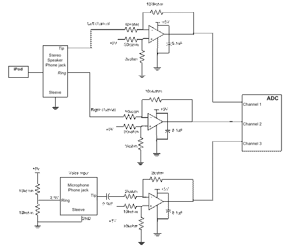
Fig 4: Audio amplifiers (please also refer to the ADC port layout in appendix)
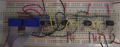
Fig 5: ADC circuit
For details please see the datasheet
3. DAC -- DAC0832
According to the datasheet two op-amps are connected to the output of DAC0832.
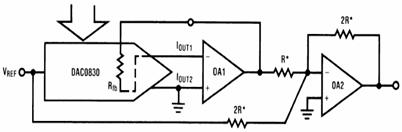
Fig 6: DAC circuit from datasheet
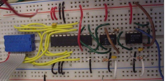
Fig 7: DAC circuit on board
Since this DAC has a current output, the first
op-amp is used to convert current to voltage. The second one is for DC shifting.
So the output can be oscillating between positive and negative as real audio
signals. The final output voltage is calculated according to this equation:
![]()
For details please read the datasheet
4. Speaker
A speaker is connected directly to the output of the above DAC. Since the sound is playback at relatively good quality, no low pass filter is used.
Note: Please refer to the bread board layout in appendix
Memory part
ALFAT is a full FAT file system precompiled and programmed on a very small but powerful 32-bit processor chip, LPC2114 ARM processor from Philips. ALFAT requires very few external components to run. For communication, a simple microcontroller with UART, SPI or I2C can be used. Therefore, Mega32 MCU used in lab can be used with the ALFAT chip since it supports both UART and SPI. In addition, ALFAT implements two modes for communication, the first one is the text mode, which is a very easy text based commands that are very similar to DOS operating system. The second mode is framed mode, which is based on data packets, and is more suited for professional applications.
Fig 8: Compact flash interface board
Karaoke Part
LCD & Button update
A LCD is used to display the current mode of the karaoke machine. One push-button is used to change the mode. When pressed, the karaoke mode will cycle through all possibilities. The calling rate of LCD and button update routine are relatively slow so that they don't affect the adc and memory operation significantly.
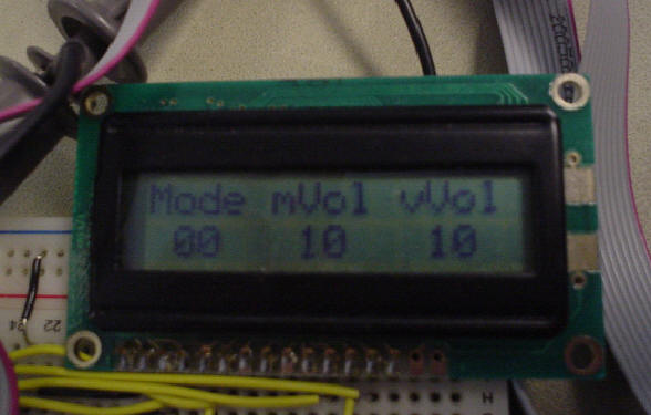
Fig 9: LCD display
ADC (SPI)
The ADC chip we purchased has a built-in SPI interface. Therefore, the microcontroller needs to use the SPI port to communicate with the ADC. During SPI interfacing, one device is designated as the master, while the other one is the slave. ADC is the the slave device. The ADC chip has four pins associated with the SPI interface, so does ATMEGA32. For ADC, CS is the chip select signal which turns the it on when low. CLK is the reference clock signal. For MCP3204, the maximum frequency allowed for the CLK signal is 2 MHz, operating at 5V. Din is the input pin which controls the ADC to convert certain input channels. Dout is where ADC sends out the converted digital result. Initiating communication with the ADC is done by bring the CS line low. If the device was powered up with the CS pin low, it must be brought high and back low to initiate communication. The first clock received with CS low and Din high will constitute a start bit. The SGL/DIFF bit follows the start bit and will determine if the conversion will be done using single-ended or differential input mode. The next three bits (D0, D1 and D2) are used to select the input channel configuration. The device will begin to sample the analog input on the fourth rising edge of the clock after the starting bit has been received. The sample period will end on the falling edge of the fifth clock following the start bit.
Once the D0 bit is input, one more clock is required to complete the sample and hold period. On the falling edge of the next clock, the device will output a low null bit. The next 12 clocks will output the result of the conversion with MSB first. The entire operation cycle is illustrated in figure 10 below.
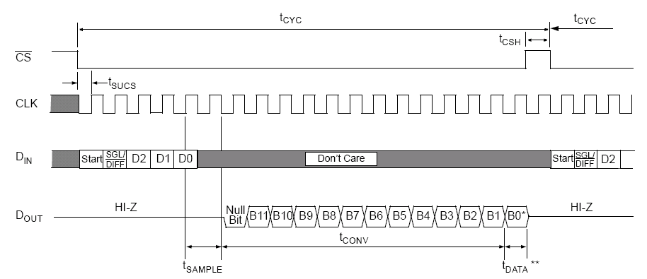
Figure 10: Communication with MCP3204
The SPI port of ATMEGA32 consists of 4 pins, PORTB.1-4. The are named MOSI(master out slave in), MISO(master in slave out), SCK and SS, which will be connected to Din, Dout, CLK, and CC, respectively. MOSI and MISO are controlled by the a function in the spi.h library. The function, unsigned char spi(unsigned char data), sends out the input argument through MOSI and collect the return value through MISO. One slight problem with this function is that the transmitted and received package are always 8-bit long. To solve this, some "leading zeros" are sent before the starting bit. The drawback for this scheme is that unnecessary clocks cycles are used, which slows down the sampling rate.
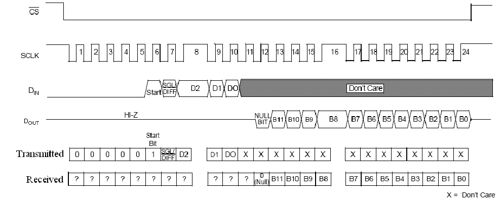
Fig 11: Communication between MCP3204 and microcontroller
The control register for the SPI is called SPCR and SPSR. They're used to enable the SPI, set up the clock rate, clock phase, and master/slave mode.
A dedicated ADC acquisition function is written to perform adc conversions. Based on the mode selected by the user, the acquisition routine will send out different channel select to the ADC. This function is called at a fixed rate by a interrupt service routine. The ISR used here is the timer0 compare interrupt. Clock has been scaled down to 250kHz by setting TCCR0 to 0x0B. OCR0 is set to 22 so that the interrupt occurs roughly every 100 ��s. This provide a sampling rate of 10kHz.
��
Memory Part
For our project, we used the UART interface to communicate between the MCU and the ALFAT chip because SPI interface is more complex, and we haven��t had exposure to it during the labs. In UART mode, UART_TX pin is used to send data to the microcontroller and UART_RX pin to receive commands from the microcontroller. The default baud rate for UART is 9600 and it is 8 bit with no parity and 1 stop bit, but the baud rate is changeable through the internal command. CTS and RTS lines must be used to insure not loss of any data. CTS pin is input to ALFAT and when it is high ALFAT will not send data and will wait for it to go low. CTS should be high as long as possible to not slow down ALFAT. RTS pin is output from ALFAT and it is set high when ALFAT 256 byte FIFO is full.
��
![]()
Figure 12: Frame Structure
We used the frame mode since ALFAT has an internal Commander that follows orders sent by the host through the chosen Control serial executes the suitable process according to the order. The frame structure is shown in figure 12. The header consists of 3-bit function indicator and a 5-bit body length indicator. Body can be 0 bytes and up to 31 bytes. Body Length in the Header must be set according to this number of bytes. Checksum is simply the sum of header and all body bytes
ALFAT provides many functions which allows various communication with the compact flash, but the ones most vital to this project are:
These functions will be explained in detail below.
Change Drive:
![]()
Figure 13: Change Drive Frame Structure
The frame structure is shown in figure 13. The header is 0xE1 as defined above, and DriveChar can be ��A��, ��B��, ��C��, and ��Z��. Drive A indicates that ALFAT is connected to either MMC or SD card, drive B represents CF is connected as a master drive, drive C represents that CF is connected as the slave drive, and drive Z represents that no device is connected to ALFAT. Since we are using compact flash card, we set DriveChar to ��B��.
Read from opened file:
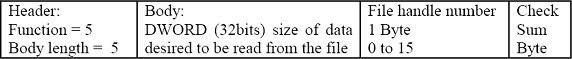
Figure 14: Read Frame Structure
The frame structure is shown in figure 14.
Reading process (File must be opened first using open file command in read mode):
Write to opened file:
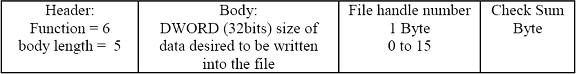
Figure 15: Write Frame Structure
Writing Process (File must be opened first using open file command in write/append mode):
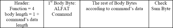
Figure 16: ALFAT command Frame Structure
The following functions are all part of ALFAT command function. These functions include the open file, close file, and set baud rate functions. The ALFAT command function has function indicator of 4, and the first body byte indicates the specific function to be performed.
Open file:
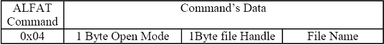
Figure 17: Open File Frame Structure
The ALFAT command, represented by the first body byte, to open a file is 0x04 as seen in figure 17.
The 1 byte open modes can be:
16 different files can be opened concurrently using file handles (0-F).
Close file:
Figure18: Close File Frame Structure
The ALFAT command, to close a file is 0x05 as seen in figure 18. This function simply closes the file represented by the file handle byte that was opened previously for reading/writing.
Set baud rate:
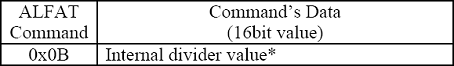
Figure 19: Set Baud Rate Frame Structure
The 0x0B command sets the internal divider registers of the UART of the LPC2114 chip. This way any possible baud rate can be set.
To calculate the divider values use![]() , where OSC is 1.47456 MHz for ALFAT.
, where OSC is 1.47456 MHz for ALFAT.
We set the baud rate to be 204.3 kHz, which yields divider value of 16. We
also need to set the baud rate of the microcontroller to the same rate so that
loss of data packets is minimal. We changed the crystal from 16MHz to
14.7456MHz so that there would be 0% error in baud rate when we change to 204.3
kHz. To calculate the UBRR value for asynchronous normal mode, we used the
equation
![]() . For baud rate of
204.3 kHz, we obtain UBRR value of 3.
. For baud rate of
204.3 kHz, we obtain UBRR value of 3.
The Karaoke part of this project works as well as we expected. The ADC acquired has a maximum sampling rate of 100 ksps. With about 16 kHz sampling, the output sound quality is as good as a regular music player output. This has proved that the noise level of the circuit is negligible. However, due to the time it requires to store the data, the sampling rate needs to drop to about 10kHz. Mode 0 has the best quality because only two channels are used in this mode which means the sampling rate is faster. At mode 1, the vocal part is also successfully removed with background music leftover.
However, when compact flash is writing data, the sound turns to be choppy this is due to the recoding time limitation.
CF/MCU Communication
Two devices, ALFAT and Mega32, communicate through UART communication system. To meet the frequency of 10KB/s, we had to raise the baud rate to 230400 bps which takes about 35us per byte. Baud rates are changed by methods described earlier. After changing the baud rate, dummy values were sent to make sure that bits were sent at correct rate and that ACK was also received at the correct rate. And with an oscilloscope we verified that bits were transmitted and received approximately at every 4.34µs which is right.
Writing to CF
Although bits can be written and retrieved every 4.34µs, we used 100µs timer0 interrupt to send data so that other tasks can be performed (such as A/D, D/A conversions). In the interrupt, data from the ADC is read at 10kb/s which is written to the compact flash using the write function described earlier. We tested with the oscilloscope that the data from the ADC indeed is transmitted to the CF at 10kb/s. However, after multiple transmissions, we found that approximately 1% of the data gets lost during transmission. This gave us some problems which will be discussed later.
Reading from CF
We had to use both timer0 interrupt and RXC interrupt. Since the buffer size of Mega32 is small, we could not permit ALFAT to send data at a baud rate of 230400bps. Interrupts were used to create timing in collecting data from Compact Flash. Timer0 interrupt was used to send data to DAC at 10kb/s and RXC interrupt was used to collect data from ALFAT. Further to avoid any loss of data from ALFAT, we used one pin from PORTD to control CTS pin of ALFAT. When CTS pin is set to high, ALFAT stops transmitting until CTS goes low. However, even though CTS pin is high, since the transmitting buffer of ALFAT is 16bytes, ALFAT could transmit up to 16bytes. We declared a small 16byte-buffer in RXC interrupt to take care of this problem. Also, to avoid two interrupts conflicting with one another, one interrupt is turned off when the other is called.
Using the oscilloscope we estimated that each bit is received at approximately 100µs which is what we expected using the interrupt.
Things that didn't work
The memory part worked perfectly except for one problem. The communication between the ALFAT chip and the microcontroller isn't perfect, and there is loss of data when trying to send a large number of packets. As mentioned above, there is approximately 1% error. To compensate for this, we sent 10 empty packets per 1000 packets sent. However, this method causes some problems in that if there is no error occurs, the empty packets get buffered in ALFAT and read as next commands. Hence, ALFAT sends ACK signal for each empty byte it receives even though these commands do nothing since there are empty packets, and during this time, MCU is merely waiting. Therefore, we get some choppiness when we playback the song from compact flash. We asked the manufacturers about this problem, and they suggested using CTS and RTS pins for handshaking, but we still had the same problem after implementation.
Safety issue
The hardware involved in this project is only the circuit part. It is safe to be used by anyone.
Usability and interface design
The purpose of this project is mainly for entertainment. Although we could not store a song into an external memory, the system still works fine as a karaoke machine. Switching between different modes can simply be done by pressing push buttons. The current function mode and volume of vocal and music are displayed on LCD. In addition to be used as a Karaoke machine, our project can also be implemented as a mixer which is able to combine multiple channels of sound in a way required by users.
Interference
Although there is another group doing Karaoke machine for this project, the way of implementation and workload for two groups are different. Other than this there is no interference with other people's design. Since we aren't using RF signals there is no RF interference from other people's designs, but since we use a microphone to record voice, there can be interference from the motor sounds of other group's projects or just noise from the room.
Overall we are satisfied with our results although it didn't work perfectly as we originally hoped. We had to spend a great amount of time researching since the project involved unfamiliar materials. The conversion of the music and voice to digital signal worked as desired and the quality of sound during playback is satisfactory. But we had some trouble writing large amount of data to memory due to time constraints. With additional time, we feel confident that we would have come up with an algorithm to compensate for the loss of data. Although we could not record songs in their entirety, we were able to record parts of it and get a better understanding of how to communicate to an external memory using UART interface using different baud rates.
Standards
For this project a compact flash will be used. Therefore, the IEEE standard of the flash drive��s format needs to be investigated. In addition, the method to communicate between the microcontroller and the drive should follow certain protocols.
Intellectual property considerations
Sample code for our ALFAT device was available on the web, but we decided not to use or modify it because they were for another microcontroller (PIC). Instead we used it as a reference by studying how they implemented some functions so that we can get a better understanding.
Ethical Considerations
Our project did not involve any aspects which involves infringement on the IEEE code of ethics. Therefore, we didn��t need to make special effort to comply with the code of ethics, but all of our actions and decisions coincided with it. The code of ethics is as follows:
1. to accept responsibility in making decisions consistent with the safety, health and welfare of the public, and to disclose promptly factors that might endanger the public or the environment;
Our project doesn't pose any danger to the public. There should be no risk in using our product
2. to avoid real or perceived conflicts of interest whenever possible, and to disclose them to affected parties when they do exist;
We believe there is no real or perceived conflicts of interest associated with our project.
3. to be honest and realistic in stating claims or estimates based on available data;
Our webpage accurately describes the procedure
and result of our project.
4. to reject bribery in all its forms;
No bribery was offered to us, and there is no reason to accept bribery for our project as our funding is sponsored by Professor Servetto's research group.
5. to improve the understanding of technology, its appropriate application, and potential consequences;
The core component of our project is recording sound with a microphone, convert it to digital signal using ADC and revert it back to analog sound signal using DAC. To understand how this technology can be used in common applications, and to improve our understanding, we decided to incorporate the idea into a karaoke machine. From the project we were able to understand the issues considered when building a karaoke machine such as determining the sampling rate so that playback would be acceptable.
6. to maintain and improve our technical competence and to undertake technological tasks for others only if qualified by training or experience, or after full disclosure of pertinent limitations;
Through the project, we have improved our technical competence. From the labs in the class, we obtained the background knowledge to start the project, and by doing the project we were able to further our knowledge beyond the scopes of the class by learning about the SPI interface, etc.
7. to seek, accept, and offer honest criticism of technical work, to acknowledge and correct errors, and to credit properly the contributions of others;
We also sought help from the professor, TAs,
classmates, and the chip manufacturers in solving the problems that occurred
during the project. From the CF interface board manufacturer, we received
assistance on how to set the filename to be read or written so that it can be
understood by the ALFAT chip used. We had a lingering problem of the chip
creating an incorrect filename, but they advised us to send a null byte at the
end of the filename which fixed the problem. To reduce the rate of packet
loss, the professor recommended that we use a crystal that had the same
frequency as that of the ALFAT chip.
8. to treat fairly all persons regardless of such factors as race, religion,
gender, disability, age, or national origin;
All members were treated equally without discrimination during the project.
9. to avoid injuring others, their property, reputation, or employment by false or malicious action;
No person's property, reputation, or employment was damaged, and we have not maliciously broken any equipment in lab.
10. to assist colleagues and co-workers in their professional development and to support them in following this code of ethics.
During the project, we have not encountered infringement in the code of ethics by anyone in the lab. Had we encountered this, we would support them in following the code of ethics. Also we will be able to assist future ECE476 students who will be working on a project similar to ours.
The code of ethics can be found in the IEEE page. Code of Ethics
Legal considerations
There are no FCC related legal considerations for our project.
Program listings
Schematics


ADC port connection

DAC port connection

DAC output connections
Cost summary
|
Item |
Quantity |
Unit price ($) |
Total cost ($) |
|
Power supply |
1 |
5 |
5 |
|
Compact flash driver |
1 |
89.95 |
89.95 |
|
Bread board |
3 |
6 |
18 |
|
Mega32 |
1 |
8 |
8 |
|
STK500 board |
1 |
15 |
15 |
|
14.7456MHz crystal |
1 |
1 |
1 |
|
MCP3204 |
3 |
5.5 |
16.5 |
|
DAC0832 |
1 |
1.47 |
1.47 |
|
Total |
$ 154.92 |
||
Table 2: Project costs
Note:
Division of labors
Considering the workload of this project, we decided to have two groups work on it together. One group (Song Du and Sining Qi) worked on the karaoke machine part which involved all the musical part, and the other group (Jae-hoon Lee and Jae Young Cho) worked on the memory part which was to write and read data to/from the external compact flash.
|
Group member |
Contribution |
|
Jae-Hoon Lee |
Recorder��coding |
|
Jae Young Cho |
Recorder��coding |
|
Song Du |
Karaoke��coding |
|
Sining Qi |
Karaoke��Hardware design and testing |
Table 3: Task distributions
References
Data sheets
Manuals
Reference Codes
Schematics
Vendor sites
National instrument
��
��
��
��
��