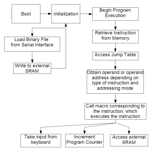
CPU Execution Sequence Diagram
The goal of this project was to develop a system capable of emulating an Apple II personal computer.
This project attempted to reconstruct a functional Apple II emulated on Atmel ATmega32 processors. Due to time constraints, a fully functional Apple II was not produced; however, a working emulated 6502 processor, memory subsystem, and partial GPU was produced.
The Apple II was the first popular microcomputer manufactured by Apple. It used a 1MHz MOS Technology 6502 processor, had 4KB RAM (addressable 64KB), an audio cassette interface for data storage (later replaced by a floppy disk drive), and color graphics capability by NTSC composite video output. Originally, it ran IntegerBASIC, a BASIC interpreter that served as its operating system. This project attempted to emulate an Apple II system without sound, using Atmel ATmega32 processors and some external hardware. Constructing a fully functional Apple II would result in a usable personal computer, capable of running vintage personal computing software as well as any new software desired when compiled to the 6502.
On a personal level, taking on this project meant that there were very clear constraints to what could be done with the direction of the project, as the only non-Apple II components must be compatible with the original Apple II in some form to qualify. The net result was a relative paucity of major hardware and software tradeoffs, which simplified the design stage. In addition, the availability of original software specific to the platform was a large draw.
In order to provide a more challenging project and to provide a modern update for future compatibility, the CPU was emulated in AVR assembly. The project fulfills the Apple II's capacity for SRAM through the use of two external 32KB SRAM chips. A GPU was implemeted in AVR assembly to use DMA (Direct Memory Access) to access the common RAM for 40x40 16 color NTSC display, as occurred in the original Apple II. Finally, PS/2 keyboard input was processed by the CPU and translated to equivalent Apple II keyboard input access on the fly. The computer as a whole can be viewed as being under the central control of the CPU, with each subsystem as subsidiary components.
Although the prototype Apple II was not fully polished due to timing constraints, each component had at least basic functionality. User interaction with the Apple II occurs through loading 6502 machine-language programs over RS-232 serial at 9600 baud, and watching the output on the TV. Once the CPU has booted, it waits for a 4-byte program size and machine language program to be loaded, and then commences operation. While the program size is in hex, sizes with components larger than 9 are not accepted; thus, programs are generally padded with 6502 "nops" to avoid this constraint. In practice, these values are calculated beforehand and sent over serial as prepared files. If serial debugging is enabled, the progress of the emulated program may be viewed in Codevision Terminal with automatic appending of linefeeds to carriage returns, in ASCII mode.
The main hardware tradeoff encountered was found in the GPU. Earlier projects implementing color NTSC had used a chip specifically for the generation of sync pulses and the NTSC color burst (the ELM304). It was determined that this chip would simplify the GPU software, but was strictly unnecessary and increased cost and hardware complexity. Therefore, it was not included in the final design.
The major standards involved in the project were the NTSC color television standard, the RS-232 serial standard, and the PS/2 serial standard. As no devices using these standards function correctly without proper implementation, not following these standards was not an option.
The usability and safety of this device is comparable to the Apple II and Macintosh computer that it is based from. The original Apple II had some important usability advancements over previous personal computers. For instance, the color display and computer casing were revolutionary at the time and have important usability implications over previous designs. Although the current prototype does not have a casing, as work continues it is not expected to be difficult to procure a satisfactory enclosure. In general, computers are enabling devices that allow disabled persons to live more productive lives.
Intellectual property considerations are important to take into account for this project. The Apple II was a proprietary system and its source code was copyrighted by Apple. In addition, the 6502 is still in production, but the patent (issued in 1975) is believed to be expired. It is also believed that a prototype emulator of this system constitutes fair use for the copyrights envolved.
The software design consisted of three segments: the 6502 emulation on the CPU, the video generation on the GPU, and the keyboard input on the CPU. As each was implemented separately and independently from each other, they will be discussed in turn.
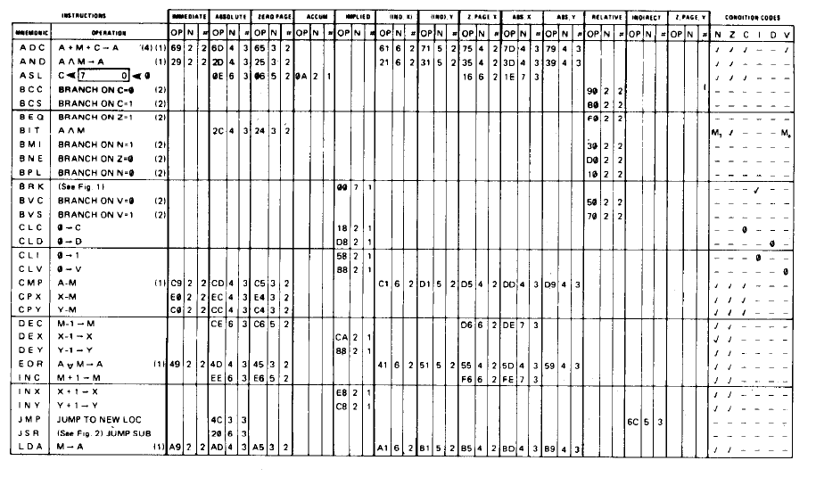
The basic structure of the 6502 emulation is to load programs into RAM, and then begin execution of individual 6502 instructions. All 6502 registers were emulated in hardware, as shown in Table 1.
| 6502 Register | Description | AVR Register(s) |
|---|---|---|
| S | Status Register
7: N (Negative) 6: V (Overflow) 5: Unused 4: B (Break flag, 1 == BRK, 0 = IRQB) 3: D (Decimal Mode Enabled) 2: I (IRQB disble) 1: Z (Result Zero) 0: C (Carry) |
R19 |
| A | Accumulator (used in many instructions by default) | R8 |
| X | Index Register (general purpose register or index value of effective address) | R2 |
| Y | Same as X | R3 |
| IR | Instruction Register - store current Opcode | R4 |
| SP | Stack Pointer | R5 |
| PC (16 bits) | Program Counter | R12(Low):R13(High) |
Although initially the majority of the CPU was intended to be done in C, it was found that the Codevision compiler had very poor optimization capabilities, and in addition limited access to similar features of the AVR to the 6502 that could be helpful. Therefore, the vast majority was written in AVR assembly. To execute an instruction, the value at the PC is loaded from RAM, and then used as an AVR address to index into a hand-coded jump table. The jump table then redirected the instruction to the appropriate execution block.
There are 151 separate operations that can be executed on a 6502 when all addressing modes are accounted for. However, there are a great number of similarities between opcodes, which allows for easy implementation. Addressing modes are shared between opcodes, and execution macros are shared between opcodes of the same type but different addressing modes. Not only does this allow ease of coding, but it also reduces the necessary number of testcases, since each addressing mode and each instruction need only to be tested once.
Although most instructions were trivial to implement, some caused considerable difficulty. The AVR and 6502 ISA's have different conventions for status register flags, and existing documentation was often inconsistent or incomplete. For instance, the 6502 natively implemented support for Binary Coded Decimal (BCD), a format where decimal numbers are stored in nibbles of binary bytes, allowing precise decimal calculations while sacrificing range. However, there are many incompatible forms of BCD, and specific documentation for the 6502 was extremely lacking. Eventually, enough references were found to ensure a precise determination of the behavior of the processor when in Decimal mode. When that was determined, it then was necessary to implement that behavior, which was fairly complicated. In the end, AVR Application Note 204, a reference implementation for BCD on AVR, was used in a modified form. This pattern, with the exception of the helpful Application Note, was repeated for many opcodes.
The final design saw most of the instruction execution code as assembly macros, and most of the addressing code as C macros.
Testing was accomplished on the CPU through an extensive suite of 6502 assembly programs, which would automatically trigger a breakpoint interrupt on an error, or infinite loop if the error was a branching problem. Each instruction was tested separately, but without all addressing modes. Then, all addressing modes were tested for a few instructions. Because of the nature of the modular structure of the emulator, this was sufficient for ensuring a high level of compatibility with the 6502.
Testing the interface to the RAM was accomplished through a simple, separate test program that, using identical code to the main CPU program, wrote values to every byte in memory and read them back, checking for accuracy. This proved invaluable when faulty connectors disrupted good dataflow between the RAM and CPU.
Although monochrome video generation was done in the previous labs, and several previous groups had done color video generation in the past, the unique nature of the GPU neccesitated a unique design. In most previous designs, the video generation processor either only used internal RAM, was the sole master of the external RAM, or had the contents of the RAM fed explicitly to it. The GPU in this project was required to have secondary, synchronized bus access to the RAM, and retrieve data itself when the CPU was not actively using it. In addition, although it was not implemented for this prototype, the high resolution mode on the Apple II GPU required much tighter control of time than an interrupt-based approach would allow. Therefore, all timing was done through clock-tick counting. This, combined with the lack of an external sync pulse generator, meant that the exact specifications of NTSC had to be known precisely, rather than just the basic data period and wait period used by many other projects. This caused many difficulties in producing proper video output, as most documentation available on the NTSC standard only describes a part of the picture.
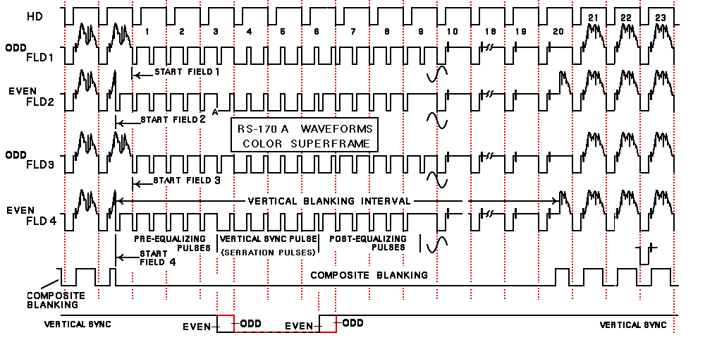
Nearly all of the GPU software was written in AVR assembly. Several timing constructs were introduced by concatenating "nops" to produce precise delays, up to a delay of 31.25us (500 clock ticks) at a time. Ignoring some basic initialization, the program can be seen as essentially consisting of a loop to output frames, with internal loops to output display lines and vertical synchronization and blanking lines. Inside each display line, a horizontal pulse was first emitted for 4.75 us, followed by the "back porch" (containing the color burst along with blanking for synchronization) for 4.75 us. Then came the data region of 45 us, which was shortened to compensate for the selected television's large out-of-bounds scan. Following that can the "front porch" of 4.5625 us, which either looped back to make another of the 242 data lines or continued on to the first 3 vertical blanking lines. These were like data lines but with a continuous black level. They were followed by three vertical synchronization lines, which were identical to blanking lines except that the vertical sync line was high, which effectively inverted the horizontal sync and suppressed the color burst. This was followed by 14 more lines of vertical blanking to make up for the remaining full 262 lines of interlaced output.
Inside the data lines, work was constantly being done. Unpacked data was stored in a special line buffer for immediate display, while raw data was stored in a larger, packed array. During the horizontal sync pulse, back porch, and front porch, the line buffer was populated anew from packed data stored in the large buffer. During the data portion, that data was read out on PORTD to produce the appropriate output. All of these operations were computationally balanced to ensure consistent timing. In addition, since the theoretical output resolution of the GPU was much higher than the 40x40 resolution used by the basic Apple II graphics mode, each pixel stored in the line buffer had to be extended to a width of 18 clock ticks horizontally and 6 lines vertically. Extending horizontally was done by delaying between changing the outgoing color value, while vertical stretching was accomplished by maintaining a counter and only unpacking the next line when the counter indicated to.
Testing the GPU was accomplished by writing test patterns to the screen and observing the results. Since the results were always clearly right or clearly wrong, no automated testing was necessary. An oscilloscope was also used to monitor the composite video output. Debugging was often difficult due to a lack of hard information about the allowable video waveforms and obscure assembly errors. Stripping out almost all traces of C eliminated many bugs, as it was determined that the Codevision compiler was stepping on important status registers to as temporary registers to perform simple operations.
The Apple II Emulator hardware is broken up into modular components, arranged for function and easy of integration. Figure # shows an abstract circuit diagram of the Apple II Emulator.
The Central Processing Unit, CPU, is an Atmel ATmega32, located on an STK500 and accessed through the I/O pins of that board. The STK500 also provides power for the other peripheral circuit boards and performs all reprogramming duties. Originally, the design called for more than four I/O ports on our CPU, so the design called for an Atmel ATmega128 to function as the CPU, which is only usable with an STK500 and attached STK501 top module, since prototype PCBs and small surface mount soldering are beyond the resources of the class. In its final configuration, four ports were sufficient to perform all CPU functions, so the change was never made to the Mega128. However, since the other modular components were designed to interface with the STK500, the CPU was not moved to a separate PCB.
The Graphical Processing Unit, GPU, performs video processing and generation for the Apple II Emulator. As seen in figure#, the GPU is a Mega32 mounted to a PCB with attached peripheral components for video generation: a digital to analog converter and NTSC encoder.
The data path of the GPU can be seen in the schematic below.
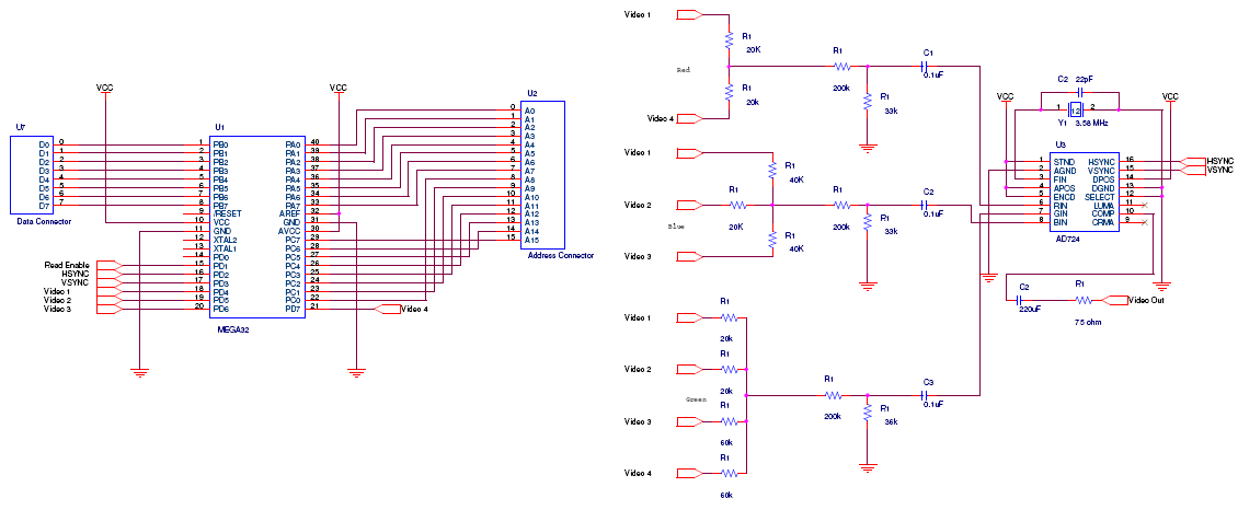
Synchronized with the CPU to avoid memory reading conflicts, the GPU has Direct Memory Access (DMA). It loads byte packed image data from RAM into PORTA of the Mega32, using ports C and D for addressing the 64KB of RAM. It then unpacks the data and readies it for output. For details on this, see the software section. The unpacked screen pixel data is then output on pins D4 - D7 to a resistor network, acting as a digital to analog converter. As specified in the Apple II manual, the GPU is capable of outputting up to sixteen different colors. These colors, along with their nibble codes and separated red, green and blue components are listed in Table 2. Note that a value of 255 indicates maximum intensity.
| color | nibble | red | green | blue |
| Black | 0000 | 0 | 0 | 0 |
| Magenta | 0001 | 128 | 32 | 64 |
| Dark Blue | 0010 | 0 | 32 | 128 |
| Light Purple | 0011 | 128 | 64 | 192 |
| Dark Green | 0100 | 0 | 96 | 64 |
| Grey | 0101 | 128 | 128 | 128 |
| Medium Blue | 0110 | 0 | 128 | 192 |
| Light Blue | 0111 | 128 | 160 | 255 |
| Brown | 1000 | 128 | 96 | 0 |
| Orange | 1001 | 255 | 128 | 64 |
| Grey | 1010 | 128 | 128 | 128 |
| Pink | 1011 | 255 | 160 | 192 |
| Green | 1100 | 128 | 192 | 64 |
| Yellow | 1101 | 255 | 224 | 128 |
| Blue/Green | 1110 | 128 | 224 | 192 |
| White | 1111 | 255 | 255 | 255 |
Using the resistor network, the 16 color nibble codes are output onto the four output pins and augmented to fit the red, green and blue components of each color. To accomplish the full color spectrum with only four outputs, each output bit must contribute to multiple color components. The portion of each red-green-blue color component each pin is responsible for is shown in Table 3. When all four output pins are high, the components each sum to 1, which generates white.
| Color \ Nibble | 4 | 3 | 2 | 1 |
| Red | 1/2 | 0 | 0 | 1/2 |
| Green | 3/8 | 3/8 | 1/8 | 1/8 |
| Blue | 0 | 1/4 | 1/2 | 1/4 |
The resistor network used to generate these colors takes advantage of the fact that using resistors of significantly higher resistance downstream from the DAC will not greatly affect its output, since much lower resistance current paths exist.
To be encoded, each component voltage must range from 0V, black, to 0.72V, white. Since the Mega32 outputs 5V in its high state, a voltage divider circuit is used the scale down the voltage. Theoretically, the resistor network should provide slightly more than .72 volts, but due to poor accuracy tolerance for resistance values and other mitigating factors, the circuit actually outputs almost exactly 0.72V. It should also be noted that the green component resistor divided should theoretically provide a higher peak voltage than red or blue. However, during testing it was noted that the green color component came through weak in the display. Modifying the observed green portion of the resistor DAC solved this problem.
After scaling, the color signals are AC coupled with 0.1uF capacitors and fed into the AD724 NTSC encoder. While past projects in ECE476 also used an ELM304 to generate a composite sync pulse and color burst, believing that the ELM304 was required for color burst generation, the AD724 is actually equipped to create this color burst alone. This represents a significant design change from previous projects. In the other projects, the ELM304 performed all synchronization duties and the MCU simply monitored the video synchronization to determine when to output data. On the Apple II GPU, both the horizontal and vertical syncs are generated onboard through pins D2 and D3, feeding them to the AD724.
Inside the AD724, the three color inputs are combined into a single composite video output along with the synchronization data. For proper operation, this output is tied to a 220uF capacitor upstream in series with a 75 ohm resistor. This output then travels to the TV.
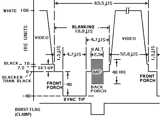
For proper video generation, each horizontal line should resemble the waveform above. In addition, every 262.5 line frame should be concluded by a vertical sync, consisting in our case of three lines of black followed by three lines of inverted syncs, followed by another 14 lines of black before video output resumes.
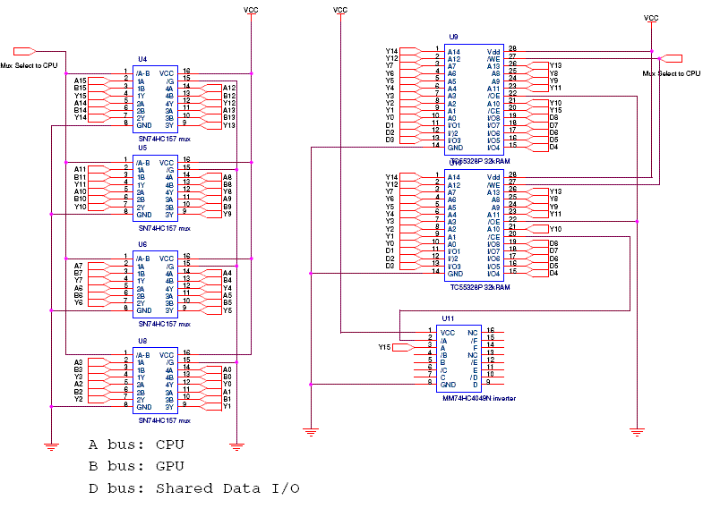
The original Apple II had up to 64K of RAM, 48k of which was addressable. The rest was used for internal ROM. The Apple II used a form of direct memory access, byte mapping data for use by other components instead of wasting processing time routing data. For the Apple II Emulator, it is necessary that the CPU have read/write access and the GPU to have read only capability. However, both boards require the ability to address the RAM. To accomplish this, the 16 bit memory addresses from both the CPU and GPU are routed through four quad 2:1 multiplexers, part number SN74HC157. The mux is controlled by the CPU. By using a single data line between the CPU and GPU, the two microcontrollers are able to avoid trying to load from memory simultaneously. To facilitate dual RAM access, the CPU muxes the memory to the GPU whenever it does not need it.
To provide the desired 64k of SRAM, the memory module holds two 32kbyte SRAM chips, part number TC55328. To convert these chips to a single 64k addressable memory module, the top address bit is fed into the chip enable of each chip, but with the signal being inverted through an MM74HC4049N inverter chip before reaching the memory. While this solution works and meets our requirements, it created a large manufacturing problem since every input and output had 2 sources and two destinations. On the data side, since the GPU only receives data from RAM and never writes to it, it is not an issue to tie both MCUs to the same I/O pins, provided that the GPU is instructed by the CPU not to read data while the CPU is using memory. A schematic of the Apple II Emulator Memory Module can be seen in the schematic below.
As a final addition to the Apple II Emulator hardware, work has begun to integrate a keyboard into the computer. A standard PS2 keyboard requires Vcc, GND, Data and Clock signals. The keyboard provides the clock, outputting a bit after each falling clock edge. To integrate the keyboard into the design, a PS2 connector was taken from a broken computer mother board, and wires were connected to the 4 required pins. The Data and Clock signals interface with the CPU microcontroller on pins D1 and D2, respectively.
During the testing of the memory, sporadic, random errors were encountered upon reading and writing data to RAM. After many hours debugging, it was determined that although the connectors we were using, bundled wires with MOLEX heads, had great electrical connectivity, they did not provide enough electrical isolation between lines. Therefore, as we were attempting to write TTL voltages to the RAM using them, electromagnetic interference was causing "random" bit-flips. This was confirmed when switching to isolated jumpers, first individual 2-pin jumpers and later 8-pin jumpers with a custom board interconnect, fixed the problem completely. Sometimes, it is not just a bad wire.
In addition, when implementing the emulated 6502, originally a simple map between 6502 assembly and AVR assembly was attempted. The problem with this is obviously that the two instruction sets, even when they share common names, oftentimes do subtly different things. For example, the carry bit for the SBC instruction on the AVR is the inverse of the carry bit for the SBC instruction on the 6502. This makes it impractical to attempt a one-to-one mapping of any kind for many instructions.
The CPU was extensively tested according to the documentation available, and passed all tests. These tests verified the functionality of all instructions and addressing modes, and therefore comform completely to the developers' functional understanding of the 6502. It is important to note that the emulator is not cycle accurate, although it does achieve parity or better speeds. However, time constraints did not permit the loading of the obtained original Apple II operating system and software, full verification has not been achieved. It is believed that with at most small tweaks, the 6502 emulator and CPU in general is ready for productive use.
The memory subsystem was thoroughly tested as mentioned above, and all components corresponding to CPU access to memory work flawlessly. However, as the GPU was not integrated onto the bus, there is no guarantee, although it is highly likely, that DMA will work as intended. This is due to the highly symmetric nature of the memory structure, and the built-in synchronization methods; in addition, it is known that memory accesses by the CPU are a very small fraction of processor time, leaving a great deal of free memory bandwidth for use by the GPU, as expected.
This was the most promising yet most disappointing portion of the project. While we were able to produce color images of better than our target resolution, a series of unexplained errors prevented complete integration into the system. As the GPU was based on a timing system, rather than an interrupt-based system, it required precise timing calculations to accurately display a picture, which were successfully implemented. However, after consultation with Professor Land, it appears that a compiler, assembler, or architecture bug caused catastrophic failure in the video output when certain non-temporal changes were made. For example, if we enacted a minor change such as converting an assembly macro of 10 cycles to a series of 10 "nops", sometimes, the video picture would be completely destroyed, even though no change should have been visible. It is believed that store instructions such as ST or PUSH, oftentimes concerning the X, Y, or Z index registers, caused this error, although no reasonable explanation has been proposed.
Despite this failure, it is clear that if this issue can be resolved, this implementation can be a stable and robust platform for high-resolution color output, that will suit this project extremely well. However, given the nature of the difficulty, it is unknown whether the current configuration is viable.
The keyboard, always a lower priority than the more important subsystems, was not completed due to timing constraints. However, test software, which should provide fast translation to Apple II keyboard codes from a standard PS/2 interface, was developed, but not used.
Since no non-COTS high-voltage components were used, and no other apparent sources of danger were encountered, safety was not a large factor in the design. Interference was also not a major concern, as any RF broadcasted was incidental.
Certain aspects of the hardware turned out to be much more difficult than believed. For instance, the memory subsystem took a considerable amount of time, even though it is arguably the simplest part of the system, mostly due to the electromagnetic interference encountered during testing. More time should have been budgeted for integrating hardware systems. Despite this, the software was more difficult and thus did need more time than the hardware.
Using more COTS components to simplify tasks would have been a great boon. For instance, even if we wanted to continue to emulate the 6502 on an AVR chip rather than using one directly, it would have been extremely helpful to have a reference implementation to test with. Also, while the ELM304 chip was not necessary and more expensive, it would have greatly simplified the GPU. A simpler GPU, even with the probable degraded performance, might have resulted in a much more complete final prototype. A better strategy, even if the more accurate on-chip NTSC sync was desired, would have been to get a baseline implementation working and then pursue the higher-level accuracy if time permitted.
Financial considerations precluded the development of a PCB implementation of the system. However, this would have been a much better solution. Constant problems with wires and transportation delayed further development, and a "motherboard" type approach would be more conducive to the end goal of a workable personal computer.
Hardware purchases should have been made earlier, with an emphasis on early implementation and testing. A design switch from VGA to NTSC a few weeks in was accomplished fairly painlessly, but that could have been an extremely difficult situation.
All standards incorporated into the project were successfully implemented.
All of the software used in the project was custom-designed and programmed, and thus has no copyright problems. As the project was to emulate a proprietary system, there are some patent considerations; however, the patent on the processor itself is believed to be expired, and no other patent information was discovered. For the remaining copyright considerations, it is believed that a project of this type is considered fair use.
| Part | Quantity | Price Per Unit | Total |
| STK500 | 1 | free—donated by CUSat | 0 |
| ATMEGA32 | 2 | free—donated by Kris Young | 0 |
| TC55328 | 1.99 | 3.98 | |
| Small PCB | 1, plus some scraps | 1 | 1 |
| Large PCB | 1 | 2.5 | 2.5 |
| Custom PCB | 1 | 5 | 5 |
| Color Television | 1 | free—borrowed from girlfriend | 0 |
| SN74HC157 Multiplexer | 4 | 0.53 | 1.12 |
| MM74HC4049N Inverter | 1 | 0.6 | 0.6 |
| AD724 NTSC Encoder | 1 | 9.65 | 9.65 |
| 3.58KHz Oscillator | 1 | 0.4 | 0.4 |
| PS2 Keyboard | 1 | free—already owned | 0 |
| PS2 Keyboard Socket | 1 | free—found on scrap motherboard | 0 |
| Total Cost | $24.25 |
6502 Firmware Info
6502 Instruction Set:
AVR Instruction Set
Misc
Video
Keyboard
Data Sheets
Code/designs borrowed from others