Data Acquisition System
With Controller Area Network and SD Card
David Porter dhp22 and Steve Gilson
spg32
Introduction
This project implements a high speed data acquisition system using Mega32 microcontrollers and a Controller Area Network (CAN).
Recording data is essential to testing and developing a racecar. Recording what each sensor is doing can tell an engineering how the car is performing, and most importantly, how to make it faster. A well outfitted car can have many sensors, with Formula One cars having well over 100 sensors. Cornell’s FSAE car has over 50 sensors on it, many of which require high sampling rates to be useful. Commercial data acquisition systems are either expensive, slow, or have few inputs. A solution to this problem had been attempted by previous 476 students (Karl Antle and Ryan Mcdaniel) using a PIC18F2585, but it was only able to log reliably at 150 Hz. Many sensors on the car require much higher sampling rates, as the sensors are recording events occurring in a very short period of time. For example, when looking at a sharp bump using rocker position the event may only last .05 seconds when driving quickly. If taking the derivative of the data a very high sampling rate is required to give useful data, at least 500 Hz. It was this need for high speed data acquisition that motivated us to create a high speed data acquisition system to replace the current one.
Our system uses multiple transmitter nodes to acquire data from sensors and transmit the data in packets over a CAN bus. Each transmitter consists of a Mega32 microcontroller, an external Analog-to-Digital converter, a CAN controller and a CAN transceiver. The CAN packets are received by a single receiver node and stored to a Secure Digital (SD) card. The receiver node consists of a 2 Mega32s, a CAN controller, a CAN transceiver, and a SD card. The goal of the project was to create a system which can record 32 10 bit ADC channels recorded by 4 Mega32s and transmitted over the CAN bus. In addition, the system should be expandable to accept CAN packets sent from other modules, such as an ECM or a standalone O2 unit. 500 Hz on the 32 AD channels was set as a goal for sampling frequency.
High-Level Design
The motivation for this project circled around the fact that high speed data acquisition using a single ATMEL or PIC is difficult when using many SPI interfaces. Controlling a SD card, 4 MCP3008 analog to digital chips and, if using a Mega32, a CAN transceiver on the SPI bus results in timing issues resulting in poor overall performance. The main issue results from the desire to sample at a regular rate. Writing to the SD card must be done in 512 byte sectors, which takes around 3.8 ms (found using a PIC18F2585 running at 40 MHz). If a regular sample rate is desired, there must always be 3.8ms in between sampling the AD chips so writing to the SD card does not disturb the regularity of sampling. Taking the AD sample time in to account, a maximum sampling frequency using one PIC or Mega32 processor is around 150-200 Hz (for the number of channels desired). For high performance systems, such as a racecar, 200 Hz is not enough for quickly moving sensors such as load cells and rocker position. To combat this problem, our data acquisition system uses many Mega32s working in parallel and series to avoid the SPI bus problems.
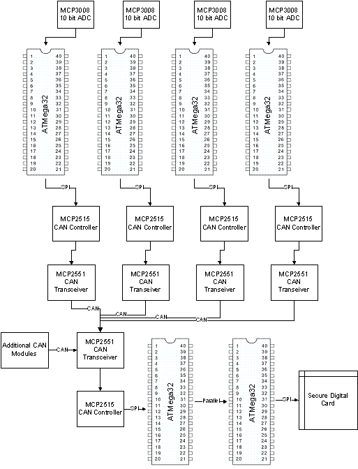
Figure 1: Data Flow Diagram
All main bottlenecks in the one chip system relate to the SPI bus. By separating the SPI bus functions among many chips, we eliminate that bottleneck in the system. As seen in Figure 1, our system uses one central unit which stores and receives data from four satellites over a CAN bus. The central unit consists of two Mega32s, one which receives the data from the satellites and one which writes the data to an SD card. The SD card is operating in SPI mode, as SD mode is a proprietary interface. The “SD” Mega32 communicates with the “Receiver” Mega32 through a parallel interface. The satellite processors handle reading the ADC chips, as well as putting the data on to the CAN bus. While these two SPI functions are controlled by the same chip, neither takes long enough to block each other when running at speeds under 2.5 kHz. As our target was much lower than this, it was deemed acceptable to use one chip controlling both SPI ancillaries.
Now that one bottleneck had been rectified, we had to ensure that the data transfer modes between chips were fast enough to meet the 500 Hz requirement. To ensure that we were going to have enough bandwidth to transmit the data through the CAN network, we calculated the number of bits required to send the data we needed to the receiving chip. To calculate this, the CAN standard must be understood.
The CAN 2.0b standard specifies the format of all packets and the encoding scheme used on the CAN bus. The CAN bus can assume one of two states, dominant (logical low) or recessive (logical high). If two devices attempt to drive the CAN bus simultaneously, one with a dominant bit and the other with a recessive bit, the bus will assume the dominant state. All devices read the value of the bus while transmitting. If a device transmits a recessive bit but reads a dominant bit, it knows that another device is transmitting and will wait until that device is finished to re-attempt its transmission. This system allows easy connection of multiple devices to the bus without any additional collision detection.
This system uses only Standard Data Frames (Figure 2). Each frame consists of a single dominant start bit, a 12-bit arbitration field used to establish message priority and identification, a 6-bit control field which includes the data length code, a data field ranging from 0 to 8 bytes, a 16-bit cyclic redundancy check (CRC) field for error detection, and a 7-bit end-of-frame field. In this standard, higher priority is given to frames with lower values of the arbitration field (dominant bits in the more significant positions).
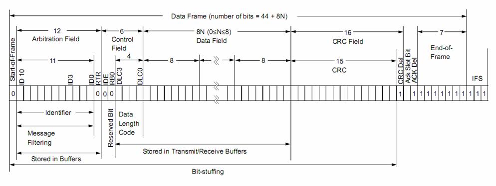
Figure 2 – Standard CAN Data Frame
Using this definition, it can be seen that only 64 data bits can be sent per packet. We will be recording 8 10-bit ADC channels in addition to 1 byte of identifier and 3 bytes of timestamp, for a total of 104 bits, or 14 bytes. To simplify the data decoding, we sent one 8 byte packet with the 1 byte identifier, 3 byte time stamp, and 4 bytes of data and one 6 byte packet with the remaining 6 bytes of data. Using the data frame depicted in Figure 2, it can be seen that since two packets are needed, 192 bits are sent total (Eq 1-3). As we would like to run 4 satellites at 500 Hz, the total data rate is 384kb/s (Eq 5).
![]() Eq. 1
Eq. 1
![]() Eq. 2
Eq. 2
![]() Eq. 3
Eq. 3
![]() Eq. 4
Eq. 4
![]()
![]() Eq. 5
Eq. 5
The maximum possible data rate according the MCP2515 data sheet is 1 Mb/s, well over the data rate required by the satellites. In addition to the satellites, there will eventually be two more units putting data on the CAN bus (not included in this project). Using equations defined above, it was found that the total data rate required for the additional two modules was a mere 27 kb/s, making the total data transfer rate 411 kb/s, still well under the CAN maximum. This gives the opportunity to clock the satellites faster in the future for a faster sample frequency.
With the CAN network calculated to be within its bounds, the other two data transfer methods were investigated. We were unable to calculate exactly what the data transfer rate of the parallel port communication was going to be, but with 8 bits transferring simultaneously during only a few clock cycles, we assumed that this would not be a problem. This assumption turned out to be correct, and is discussed in the results section.
Clocking the SPI interface to the SD card at 8 Mhz, we can assume a hard maximum data rate of 8 Mb/s. However, it is know from previous experience with SD cards that the actual data rate is often 2-5 times slower due to the processor setting up and sending the SPI information. Even with a 5 time reduction in speed, the data transfer rate to the SD card is still 1.6 Mb/s, well over the requirement. This was deemed sufficient for our purposes.
Hardware Details
Satellite Hardware
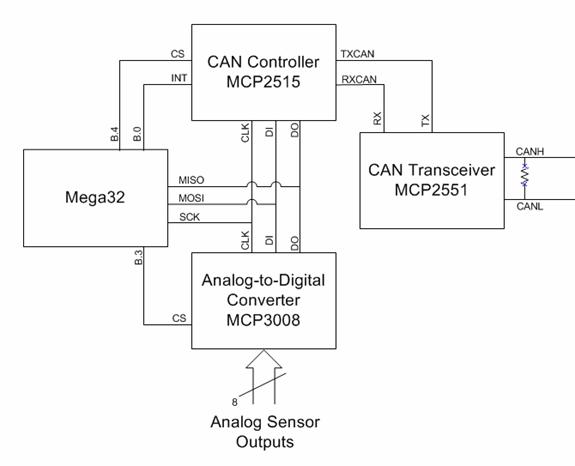
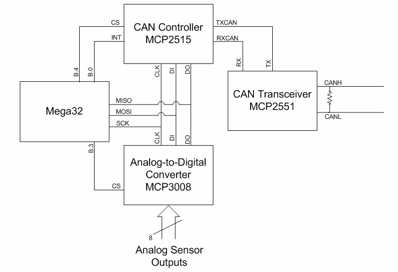
Figure 3: Satellite Schematic
Figure 3 shows the configuration of each satellite node. Sensor data is converted to digital form by the ADC, then read into the Mega32 and prepared for transmission over the CAN bus. The Mega32 loads the data into the CAN controller for transmission through the transceiver over the CAN bus.
Analog-to-Digital Converter – The system uses an external 8-channel ADC to acquire data from sensors with analog voltage outputs. The digital data is transmitted to the Mega32 using the SPI bus. Pin B.3 is used as the chip select for the ADC.
CAN Controller – The Mega32 sends the data acquired from the ADC to the CAN controller after preparing it for transmission (more in the Software Details section). Communication between the Mega32 and the controller also uses the SPI bus, with pin B.4 as the chip select. Pin B.0 connects to the interrupt line on the CAN controller. The CAN controller generates an interrupt on this line when a CAN packet has been transmitted, which is used to tell the Mega32 when to begin loading the next packet for transmission.
CAN Transciever – The transceiver functions to change between logical high and low signals (5V and 0V, respectively) on the CAN controller side and differential signaling on the CAN bus side. The external resistor functions as the load for the transceiver and is approximately 100 Ω.
Figure 4 shows a photo of the physical layout of a single satellite’s controller, transceiver and ADC. The controller is on the left, the transceiver in the center, and the ADC on the right. Figure 5 shows a photo of two complete satellites, including the Mega32s.
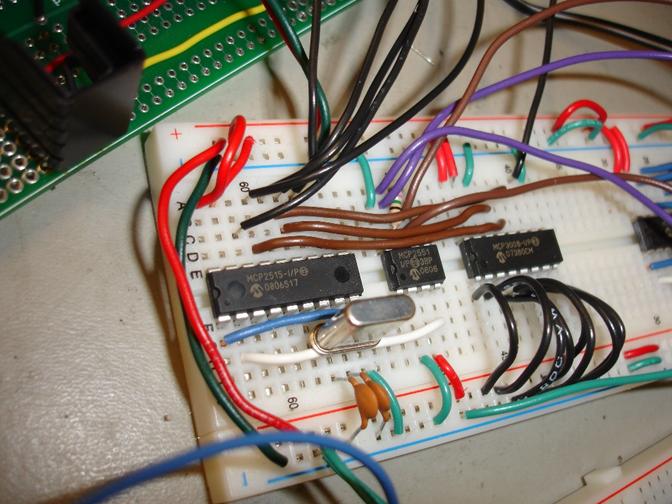
Figure 4: Controller, Transceiver and ADC for a Satellite
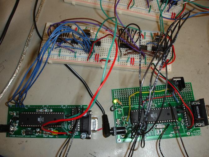
Figure 5: Two Complete Satellites
Receiver/SD Hardware
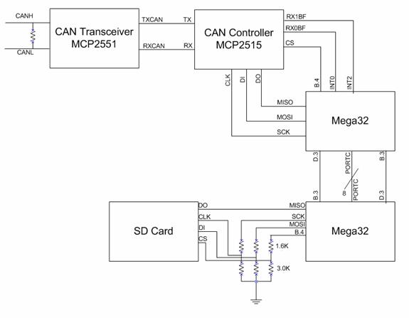
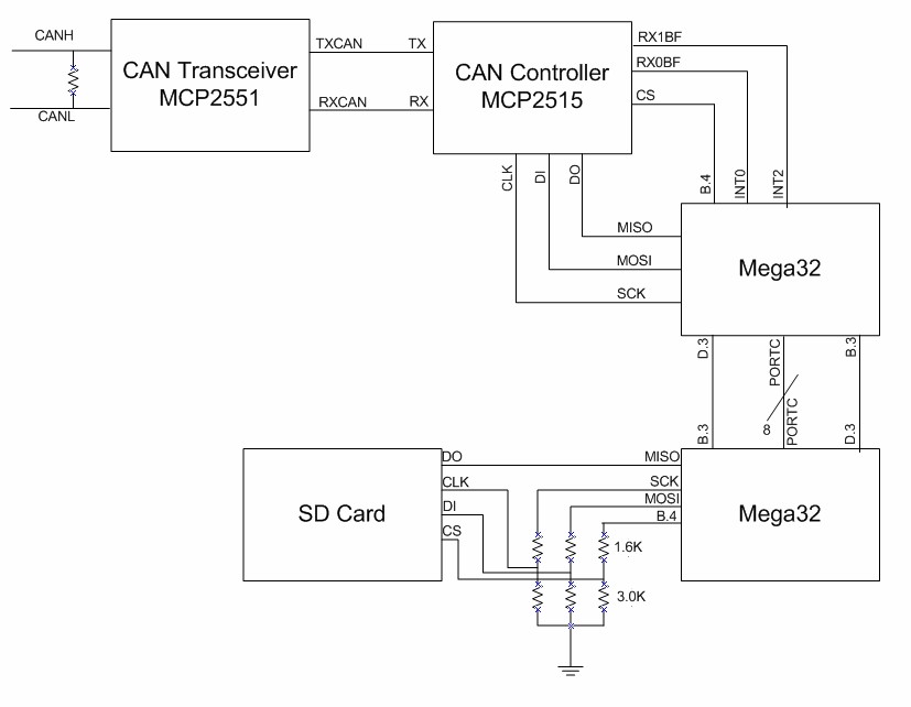
Figure 6: Receiver/SD Schematic
Figure 6 shows the configuration of the receiver and the SD card. Data is received from the CAN bus by the first Mega32 then transmitted over a parallel bus to the second Mega32, which writes it to the SD card using SPI.
CAN Transceiver – The transceiver converts differential signals on the CAN bus to 5V logic levels for the CAN controller. The packets are sent to the controller on the RX line.
CAN Controller – The CAN controller receives packets from the CAN transceiver and stores the data in its receive buffer registers. A packet reception triggers an interrupt on the RX0BF line, which is connected to external interrupt 0 on the Mega32. An external interrupt on the Mega32 causes the microcontroller to begin reading the data from the controller via the SPI bus.
SD Card Connection – The SD card uses a 3.3V supply separate from the 5V supply used by all other chips. In order to change the Mega32’s 5V logic-high levels to 3.3V levels, simple voltage dividers are used on the SCK, MOSI and CS pins. The MISO line connects directly from the SD card to the Mega32: since the 3.3V level is high enough for the Mega32, no level changer is required.
Figure 7 is a photo of the receiver and SD setup. The receiver (green protoboard) reads CAN messages from a CAN controller (not pictured) and transmits them to the SD Mega32 (yellow protoboard) via the parallel bus. This Mega32 writes the data to the SD card via the SPI bus.
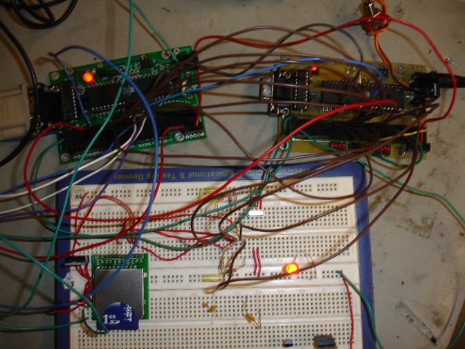
Figure 7: Receiver Mega32, SD Mega32 and SD Card
Software
Details
Satellite Software
Reset Time
At reset, the satellite initializes the SPI, Timer0, Timer2 and External Interrupt 0 control registers. The SPI interface is enabled, the SPI ISR is disabled, the MSB transmits first, and the Mega32 is configured as the master. The USART is configured for 9600 baud with Tx and Rx enabled, and the Rx complete ISR is enabled. Timer0 is configured in compare-match mode to generate an ISR at 500 Hz, which will be used to trigger data acquisition and transmission. Timer2 is configured in compare-match mode to generate an ISR at 1000 Hz, which will be used to generate the timestamp for CAN packets. External Interrupt 0 generates an ISR on a negative edge on pin D.2, which will be used to start data acquisition.
CAN Controller
Initialization
Before data can be transmitted over the CAN bus, the controller must be properly configured. All communication between the Mega32 and the CAN controller is via the SPI bus running at 8 MHz. The functions to read from and write to the controller are stored in the custom header file mcp2515.h. The controller is set to normal operation mode (at reset it enters a configuration-only mode by default). It is configured to generate an active-low interrupt on its INT pin when a transmission has completed. The CAN packet identifier is defined in the code, which is loaded onto the controller. The controller is also configured to not receive any CAN packets transmitted by other satellites by setting its receiver filters.
Main
The satellite’s main loop checks the values of three flags and launches the appropriate function if a flag is set. The poll_ADC flag is set by the Timer2 compare-match ISR every 2 ms. The flag will not be set until the EXT_INT0 ISR has run once. The external interrupt starts data acquisition, which will proceed at 500 Hz from that point forward. The ADC_buffer_full flag is set once the ADC has been read and the data is ready to be formatted for CAN transmission. The CAN_buffer_full flag is set once the data has been formatted and can be transmitted.
Analog-to-Digital
Converter
When the poll_ADC flag is set, the Mega32 will read the ADC’s eight channels in succession by calling the function spi_adc(char). It takes as an argument the channel to read and returns the 10-bit value. This function is in the custom header file mcp3008.h. The ADC reads are done using the SPI bus at 4 MHz. After the eight reads, the eight 10-bit values are stored in a buffer on the Mega32, the ADC_buffer_full flag is set and the poll_ADC flag is cleared.
Data Formatting
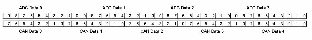
A CAN packet can carry up to 8 bytes of data, or 64 bits. Since there are 80 bits of data (8 samples x 10 bits/sample), a minimum of 2 CAN packets are required for each set of ADC values. The eight 10-bit values are formatted as ten 8-bit values and stored into another buffer on the Mega32. Figure 8 illustrates this formatting for the first four 10-bit values. The last four are converted in an identical manner. After this conversion has completed, the ADC_buffer_full flag is cleared and the CAN_buffer_full flag is set.
|
|
|
Figure 8: 10-bit to 8-bit Conversion |
CAN Transmission
The Mega32 transmits the 10 bytes of sensor data along with a 1-byte identifier and a 3-byte timestamp. The first CAN packet contains 8 data bytes: the identifier, timestamp, and the first 4 bytes of sensor data. The second CAN packet contains the last 6 sensor data bytes. These 14 bytes will be written in order to the SD card. The identifier and timestamp are included to make the data understandable to the user by telling them which satellite the data originated from and at what time. The Mega32 loads the TXB0 transmitter data length code and data buffer registers on the CAN controller and then initiates transmission by setting the TXREQ bit in the TX0CTRL register. The Mega32 waits for the transmission to complete by looping until it receives the transmission complete interrupt from the controller, which connects to pin B.0. Pin B.0 is configured as an input with the pull-up resistor turned on, so the external interrupt drives the pin low. After sending the first packet, the Mega32 clears the interrupt flag, loads the last 6 data bytes and transmits them in the same way as the first 8 bytes. Once transmission has completed, the CAN_buffer_full flag is cleared.
Receiver Software
CAN Initialization
CAN initialization consists of setting three registers using the SPI bus. The SPI bus is set up the same as detailed in the satellite software section. The device status register is set to 0x7 for normal operation, and the RXB0CTRL (Receive Buffer 0 Control) register is set to 0x60 to ensure no filters or masks are on. The third register enables RX0BF as an interrupt, which connects to INT0 on the Mega32. The SPI setup remains the same as in the Satellite initialization.
External Interrupt 0 is enabled by setting bit 1 high in the MCUCR register on the Mega32. Setting the GICR register to 0x80 turns on the enabled external interrupts.
Parallel Transmission Initialization
The parallel data transfer system requires that INT1 be set as described above. This interrupt is set the same on both the “receiver” Mega32 and the “SD” Mega32 (See Figure 6). This external interrupt will be triggered by the parallel processor when data can be written or correspondingly, read. DDRC is used as the parallel port and is set as an output on the receiver side and an input on the SD side.
CAN Receiving
When CAN messages are present on the MCP2515, a flag is set which interrupts INT0. INT0 correspondingly sets a flag which allowing the message to be read at the next convenient time. The message is read using get_msg(), which stores the data in msg_buffer. As the messages are different lengths, the lengths are compared to ensure that an error hasn’t occurred during reading. If the current message is the same length as the previous message, the current message gets thrown out. If the message buffer is full the message is not removed from the MCP2515 until the buffer has been cleared. The identifier and time stamp are all saved in the message buffer. When the buffer is full a flag is set to initialize the creation of a data buffer. The same events occurs with the second message buffer on the MCP2515, except INT2 is triggered when a message is ready, and get_msg_1() is the function called to read it.
Load_data_buffer() parses the data from the message buffers and adds the data to a 512 byte long data array which is suitable to send to the SD Mega32. When this data array fills, it is sent using parallel communication to the SD Mega32.
Parallel Communication
The parallel communication between the CAN receiving (CAN Mega32) Mega32 and the SD card writing (SD Mega32) Mega32 is extremely important, as it allows very quick transfer between the two chips. To initiate the parallel communication, the SD Mega32 toggles the INTO pin on the CAN Mega32 until a byte of 0xFF is sent. The communication has now been initialized, with the SD Mega32 waiting for the next byte to be sent. When the data_buffer is full it is transmitted by setting PORTB.3 high, setting PORTC to the next byte to send and then setting PORTB.3 low. This triggers INT0 on the SD Mega32. This interrupt sets the p_ready flag, which allows the Mega32 to store the port. When it has finished reading PINC, the SD Mega32 toggles PORTB.3 to interrupt the receiver Mega32. This process continues until all 512 bytes have been sent.
When 512 byes have been sent the SD Mega32 the SD write cycle begins.
SD Software
Setup
The Secure Digital card must be operated in SPI mode, as the two and four pin SD modes are proprietary and are expensive to purchase. When using an SD card, the SPI bus can be clocked up to 25 MHz, which exceeds the maximum that the Mega32 can output. As the maximum possible data transfer rate is desired, the SPI SCK was set to Foc/2. This is accomplished by setting the lower two bits of the SPI Control Register (SPCR) to 00, and the SPI2X bit to 1. With the Mega32 running at 16MHz, the SPI bus is then running at 8MHz. PINB.2 was used as the chip select for the SD card, and the MOSI, MISO, and SCK pins (PINB.5-7, respectively) were used.
Initialization
To begin transmission to the SD card, the chip must first be reset. This is accomplished using the SD_Reset function. This function first wakes up the SD card with clock pulses while the SD chip select is high. The chip select is then set low and the “go to idle state” command is sent to the SD card using the SD_Command function. SD_Command issues a one byte command to the SD card, then a 4 bit address (if needed for the command) and then a second 1 bit command. Padding bytes to ensure the SD card is ready and finished are added to both sides of the command bytes. The last bye is returned from the function. SD_Reset will repeat the “go to idle state command” 1000 times, at which is returns an error code. If there is no error going in to the idle state, the idle state is then checked using SD_Command again, repeating in the same manner. An error is also returned if there the card is not in idle mode. If no errors occur, the sector size is set to 512 bytes, the cycle redundancy check is turned off, SDCS is set high, and zero is returned. The SD_Reset function is repeated until it is successful. This can often take a long time to complete, though usually less than a second. Once the SD card is reset, normal operation can begin.
Data Transmission
Data transmission to the SD card is actually very simple once the chip is reset. When a data buffer is filled, the SD_Write function is called and parallel transmission is halted (see Parallel Communication). The present_sector (which defaults to 400 at reset), left shifted 9, is passed to SD_Write. The address must be left shifted 9 because the address in code is what sector we want, where as the SD card uses offsets, which are a multiple of 512 greater. Shifting by 9 effectively multiplies by 512. SD_Write commands the chip to be in write mode at the specified address. Several Paddin bytes are added to ensure that the SD card is ready, and then the write start flag, 0xFE, is sent. The 512 bytes of sector_array_AD then follow. Instead of writing a repeated function, the data transmission code here is written out in full to ensure fast execution. It was found that by removing a for loop and the function call, around a 25% increase in write speed could be achieved. Once the data has been transmitted and padded, the program waits for the SD card to be ready again, which occurs when it returns anything other than 0xFF. The card is then deselected and the data buffer index is set to zero.
References
The SD card code references code written by Karl Antle and Ryan McDaniel in 2006. Their code was written for a PIC but included all of the correct command characters for the SD card, which proved invaluable when ensuring that the correct commands were being sent. These commands were verified during debugging in the SD_SDIO spec sheet, put out by the SD Association.
Results
The logger was tested running two satellites at 500 Hz with no apparent missed sectors or delay. Data was verified using WinHex. Figure 9 shows data collected from two satellites simultaneously. One satellite has the identifier 0xBB, the other 0xAA. Starting with the first byte, we see the identifier (0xBB), the timestamp (0x01, 0x27, 0xC9), followed by 10 bytes of data. Data from the other satellite follows this, with the identifier 0xAA at position 14. The gray horizontal line in the figure indicates the end of a sector. The last bytes of the sector are not written, and the next data set starts at the beginning of the next sector. The system was not verified using 4 satellites, but the functionality and operation of four is the same as with two, and there was certainly bandwidth to spare on both the CAN bus and in the SD card transmission.
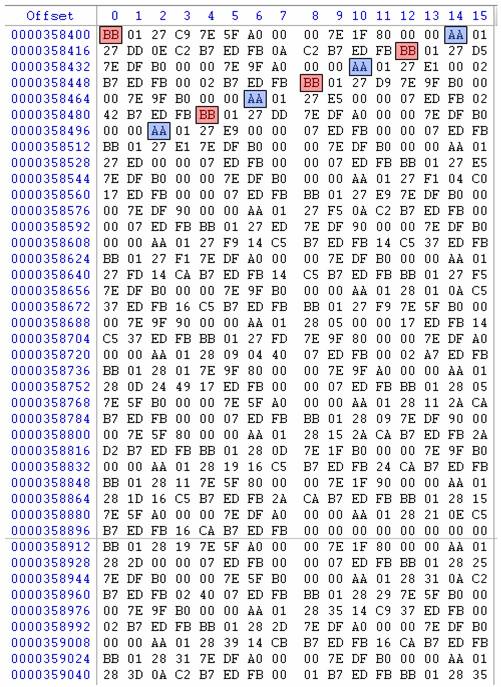
Figure 9: Data Written to SD Card by 2 Satellites
The satellites performed as expected, with the ADC read cycle taking 156 µs and the CAN transmission from start to finish taking 283 µs. These can be seen in Figure 10, where the blue line is ADC chip select and the yellow line is CAN transmitter chip select. There is a slight preparation step for the CAN transmission taking 27 µs, which can be seen as the gap between the end of the ADC chip select low and the beginning of the CAN transmitter chip select low.
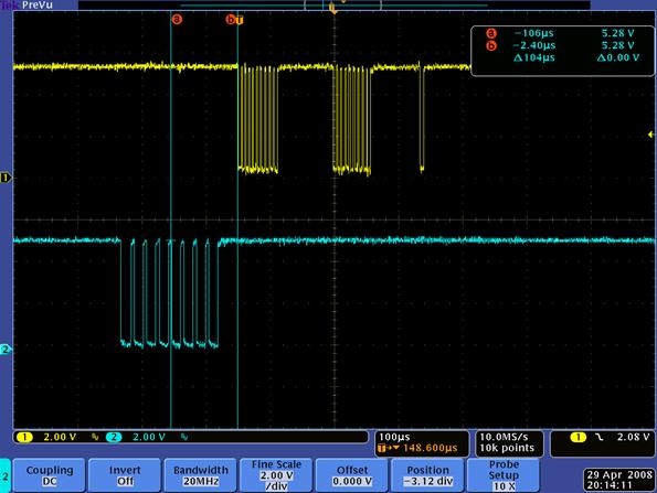
Figure 10: ADC Read and CAN Transmit Timing
The satellites also sampled at a very regular rate, which can be seen in Figure 11. The interrupt calling the sample is set to trigger at 500 Hz, which is exactly what was verified on the scope. A regular sample rate is very important for a data acquisition system and was one of the main goals of this project.
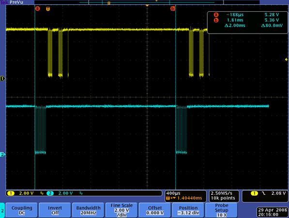
Figure 11: Time Between ADC Reads
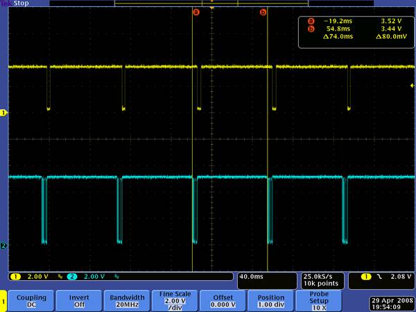
Figure 12: Time Between Parallel Reads
We verified that the parallel and SD card were operating by scoping the chip selects on both. In Figure 12, the parallel interrupt on the SD chip is blue and the yellow trace is the SD chip select. This shows how the SD controller spends most of its time idle, waiting for more information to be sent. In addition, it shows how quickly the parallel communication can take place, as it is on the same magnitude
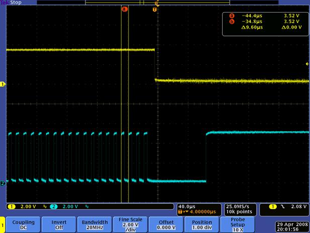
Figure 13: Parallel Bus Timing
Figure 13 shows one of the interrupts for the parallel bus as the blue trace. Each parallel read takes only 9.6 µs, and reads an entire byte.
Conclusions
Expectations
In the proposal, we set an expectation to build a system with four satellites transmitting data to a single receiver, which would write the data to an SD card through a PIC18F2585. The anticipated data rate was 500 Hz. We developed a system with two satellites transmitting simultaneously to a single receiver. We modified the original plan to use a PIC to write to the SD card and instead used another Mega32 to write to the SD card. We did achieve the data rate of 500 Hz for the system with two satellites and we anticipate that additional satellites could be added to the CAN bus and still maintain the same data rate.
While working on the project we wasted a large amount of time trying to get the PIC working with our system, for the reason that the existing CAN bus system used by the FSAE team uses a PIC to write to the SD card. In the end we did not use the PIC and instead used another Mega32 because we were much more familiar with the Mega32’s hardware and software. We could have saved a lot of time by using the Mega32 from the start and not working on the PIC at all. We adapted the SD card access code from the PIC to the Mega32.
Due to the large number of microcontrollers and other chips in our design, sloppy wiring became a major slowdown later in the project as the system grew in complexity. We believe loose wires were to blame for several fluke problems we observed while working on the project. We likely could have avoided some of this difficulty by focusing on clean wiring from the start.
Standards
Our system conforms to the CAN 2.0b specification, which describes the differential signaling on the CAN bus, the Non-Return-to-Zero (NRZ) encoding, and the dominant and recessive bit values. All of the CAN frame encapsulation is handled by the MCP2515 controller. All of the differential signaling and encoding is handled by the MCP2551 transceiver. The controller and transceiver implement the CAN specification automatically to ensure interoperability with other CAN devices. This operation is transparent to the user of the system.
Intellectual Property
The non-blocking, interrupt-driven USART functions used in the project were developed by Bruce Land and downloaded from the ECE476 webpage. The functions to read and write the SD card were originally developed by Karl Antle, Ryan Mcdaniel and Simon Wong for use on a PIC18F2585 on the FSAE team. These functions were adapted for use on the Mega32 by David Porter. All other code is the original creation of the team members. We do not plan to patent this project.
Ethical Considerations
This project does not use any radio frequency communication, so it does not interfere with any other radio frequency equipment. We have included a power LED on the SD card breakout board so that the user always knows whether the power to the system is turned on. This prevents them from connecting or disconnecting an SD card while the power is on. All control of the system is either from a PC via USART or by flipping switches connected to two of the microcontrollers. The user is not exposed to dangerous voltages through either of these interfaces. We expect this project to perform at the current data rate with up to four satellites attached to the CAN bus, however, this has not been tested. Based on measurements made with two satellites, there is sufficient time between data transmissions to allow additional satellites into the system with no additional delay.
Legal Considerations
This project does not use any radio frequency communication, so it is not subject to any FCC regulations. This project does not knowingly infringe on any existing copyrights or patents.
Appendices
Source Code
MCP2515 CAN Controller functions
Schematics
Parts List
|
Part |
Total Qty |
Qty from Source |
Source |
Price |
|
Custom PCB |
4 |
1 |
ECE476 Lab |
5.00 |
|
|
|
2 |
Borrowed from CU Minesweeper |
free |
|
|
|
1 |
Borrowed from FSAE |
free |
|
Mega32 |
4 |
1 |
ECE476 Lab |
8.00 |
|
|
|
2 |
Borrowed from CU Minesweeper |
free |
|
|
|
1 |
Borrowed from FSAE |
free |
|
DIP40 socket |
4 |
1 |
ECE476 Lab |
.50 |
|
|
|
2 |
Borrowed from CU Minesweeper |
free |
|
|
|
1 |
Borrowed from FSAE |
free |
|
DIP20 socket |
4 |
4 |
Borrowed from CU Minesweeper |
free |
|
MAX233CPP |
4 |
4 |
Sampled |
free |
|
RS232 |
4 |
4 |
Borrowed from CU Minesweeper |
free |
|
Whiteboard |
2 |
2 |
ECE476 Lab |
12.00 |
|
MCP2515 |
3 |
3 |
Digikey |
8.94 |
|
MCP3008 |
2 |
2 |
Digikey |
5.80 |
|
MCP2551 |
3 |
3 |
Digikey |
4.35 |
|
16MHz crystal |
7 |
1 |
ECE476 Lab |
free |
|
|
|
6 |
Borrowed from CU Minesweeper |
free |
|
22pF cap |
6 |
4 |
ECE476 Lab |
free |
|
|
|
2 |
Borrowed from CU Minesweeper |
free |
|
SD card slot |
1 |
1 |
Borrowed from FSAE |
free |
|
SD card |
1 |
1 |
Borrowed from FSAE |
free |
|
Power supply |
1 |
1 |
Borrowed from FSAE |
free |
|
Power supply |
1 |
1 |
Borrowed from CU Minesweeper |
free |
|
Header pins |
lots |
lots |
Borrowed from CU Minesweeper |
free |
|
|
|
|
|
|
|
|
|
|
Total Price |
44.59 |
Task List
|
Write Mega32-MCP2515 SPI interface |
Steve |
|
Write Mega32-MCP3008 SPI interface |
Dave |
|
Write Mega32-Mega32 Parallel interface |
Dave |
|
Write Mega32-SD SPI interface |
Dave |
|
Create USART debug interface |
Steve |
|
Generate and receive CAN packets |
Steve |
|
Put it all together |
Both |
|
Create webpage |
Both |
References
Standards
Datasheets
Microchip MCP2515 CAN Controller with SPI Interface
Microchip MCP2551 CAN Transceiver
Microchip MCP3008 Analog-Digital Converter with SPI Interface
Code References
USART Communication with Mega32 (ECE476 Website)