Introduction and Rationale
We used our ECE 4760 final project as a platform to develop a proof of concept for Mivo. Mivo is a low-cost, stripped down mobile payment system. Our prototype combines Radio Frequency Identification (RFID), Security Pin Authentication and Ethernet Data Transfer to provide a prototype for a low-cost secure payment system that has the potential to change lives in rural areas of developing countries.
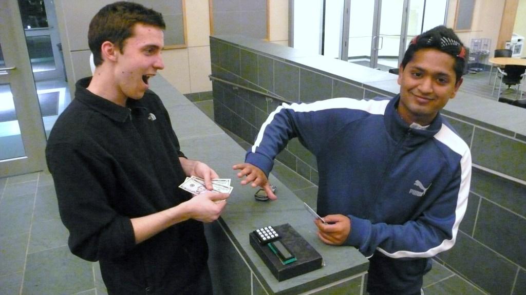
Harry and Harsh with Mivo (No cash please!)
The Idea:
Mivo is a service that aims to securely and conveniently move retail banking and financial services to cell-phones. It is a mobile-banking facility for the unbanked. We propose to deliver access to financial services to the unbanked, on low-end mobile phones. Worldwide there are 4.1 billion cell-phone users compared to just 1.6 billion people with bank accounts; further, research reveals a potential of $250 billion in micro-finance in the world, yet only $25 billion has been lent out. Mivo has the potential to bridge both gaps.
This is an idea targeted at developing countries; as the Internet and ATMs are unavailable in rural areas and penetration is low even in urban areas there are many problems faced (including access to financial services and remittances). The idea is to construct a complete mobile-payment ecosystem comprised of RFID-enabled phones and text message (SMS) transactions to access a virtual account- a simple, fast and safe solution for financial transactions. While Mivo can be a life-changer in the developing world, it also has awesome applications in the developed world. As an example application, Mivo users would be able to pay for an airline or movie ticket by text-messaging an advertised SMS code and then skip the line at the counter by scanning their RFID-equipped phone at the entry point and entering their authentication details.
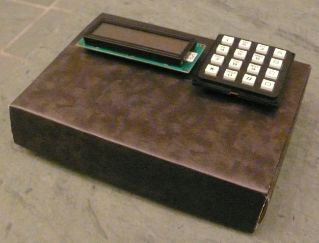
Our Mobile Payment System
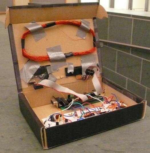
Inside Our Mobile Payment System (without the Ethernet Module)
High Level Design
We envisioned that the tasks of a generic technological payment system are:
- Identification
- Authentication
- Database access and update
Identification:
After considerable contemplation and debate we decided that we would use RFID (Radio Frequency Identification) for Identification. We selected RFID because this standard has a fairly short-range connection, a small connection-setup time (both of which make it slightly tougher to hack than some other standards) and also because we knew that our Cornell Cards have RFID tags embedded within them. Thus, we would be able to use these cards for identification instead of investing in RFID tags.
Authentication:
We decided to use 4-digit security pin for Authentication because we wanted a system that is quick and convenient while being secure. We had also considered adding a Fingerprint based authentication; however, due to the time constraint of 5 weeks we decided that we would add this feature later.
Database access and update:
Now for the Database access, while we would eventually want to transfer data over airwaves (in order to exploit the existing telecommunication infrastructure and avoid the hassle of setting up Ethernet connections), for the purpose of this project we decided to use Ethernet based data transfer. We took this decision because neither of us is familiar with 2G or 3G standards and implementing this in 5 weeks would have been a stretch.
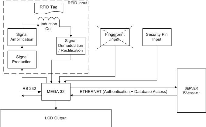
Top Level System Architecture (from Project Proposal)
Going into this project we were both really apprehensive of how much we would be able to achieve, but as advised by Professor Bruce Land and our TA Yuchen Zhang, we divided up our (Goliath-of-a-) project into sub-tasks. Neither of us has taken a course on RFID design; however we researched online to find a host of resources to help us on our circuit and data-analysis. In fact we found the documentation on Proximity Security System (project by Craig Ross and Ricardo Goto, Spring 2006) extremely helpful in selecting our design methodology. Their page also linked us to [Jonathan Westhues Proximity website] and the [microID 125kHz RFID System Guide] which provide some solid documentation on designing secure proximity systems. We had used the LCD and keypad in previous labs and hence we referred to Prof. Lands code: LCD and keypad. Eventually after many hours of research we were lucky to come across Brian Bryces website (please refer to the Acknowledgements section) which served as a good reference for us while we were designing our Ethernet system. We decided to use the Atmel Mega 16 microcontroller (as opposed to the Mega 644 that we had used in all of our labs during the semester) simply because we did not need much on-chip memory and the Mega 16 would count as a free chip in our budget (of course, we were also comfortably under-budget).
Overview:
At the top-level, we wrote a state machine that controls the working of the entire system and integrates the various subsystems into a single entity. We will go into the details of the state machine later in the Logical Structure section of our report. However, it is important to understand the top level working of the system. After the cashier enters the amount using the 4x4 keypad the state machine transitions to the RFIDInput state, which triggers the RFID system. Our system uses an inductive-antenna coil to activate the RFID tag in our Cornell ID cards and then reads off the response from the card. This response is put through a bandpass filter and wave rectification filter and finally some digital logic (more on this in the RFID section of our report) before it is fed to the Atmel Mega16 microcontroller, which further decodes the data to extract a unique code that is consistent across multiple tries for each RFID tag. Then the user is prompted to enter his/her security pin. This data and the user entered security-pin are transferred to an Ethernet Controller (connected using an SPI interface) which accesses a mySQL database through an Ethernet connection (for the detailed implementation please look at the Ethernet section of our report). A program at the backend server replies with a Good G, or Bad B message. All the user-prompts and data output are displayed on a 16x2 LCD screen and all input (at Point of Sale, i.e. front-end) is through a 4x4 keypad.
Logical Structure
A state machine controls how the entire system works. We decided to use this topology because we were going to use a state machine (from Bruces keypad code) to debounce a button-press on the keypad and extending this structure to control the various sub-systems of our project seemed a logical next step.
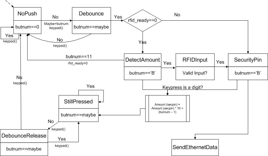
Our State Machine (Program Control) (Click Here for Full Size)
Our program starts up in the NoPush state. If a key is pressed it moves to the Debounce state (which occurs after an interval of time equal to debounce_interval set to 30 milliseconds). We used a 4x4 keypad and we had to debounce the keypad because electrical contacts in mechanical pushbutton switches often break contact multiple times when the button is first pushed. The debouncing logic removes the resulting ripple signal, and provides a clean transition. The idea here is that the bouncing of the switch will stop after an interval of 30 milliseconds.
We assign a signal called “rfid_ready” to determine which state to transition to next. A value of rfid_ready = 0 means that this is a new transaction and the state machine transitions to the DetectAmount state prompting the cashier to enter the amount. After the cashier types in the digits using the keypad he/she can confirm by pressing “B” (corresponding to butnum = 12). At any time the system can be reset by pressing “A” (corresponding to butnum = 11).
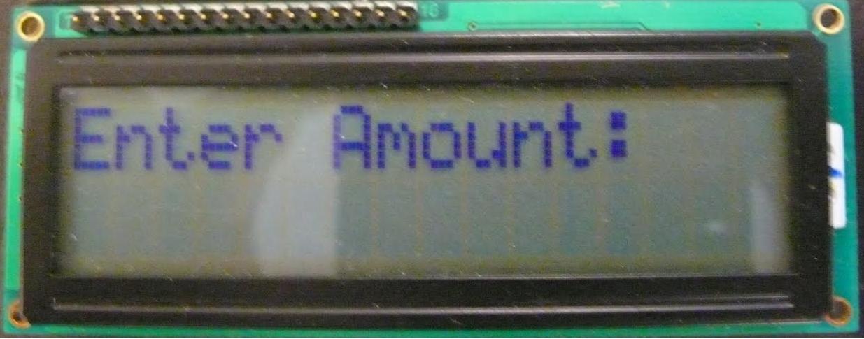
Merchant Prompted to Enter Amount
A value of rfid_ready = 1 means that amount has been entered already but there was an error in entering the security-pin (i.e. user entered an incorrect pin and pressed cancel or entered a pin that is not 4 digits long). In this case the system asks for the authentication details again.
Next, the RFIDInput state is entered and this triggers the system to get into the RFID tag identification state. This is a major subsystem of our project and will be explained in detail in the “RFID” section of our report. The RFID system outputs the bitstream read off the RFID tag and the state machine then transitions to the SecurityPin state.
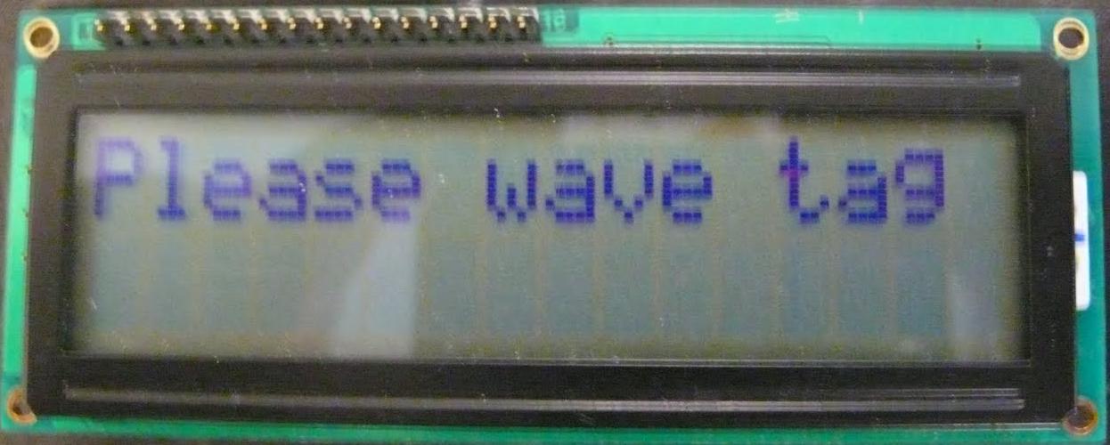
User Prompted to Wave Tag
In the SecurityPin state the user is prompted to enter his/her security-pin. The working of this state is pretty straightforward. If the user enters a pin that is not 4 digits long and confirms the system prompts the user to re-enter his/her authentication details and the system transitions to the RFIDInput state. Else, if the pin is in the correct format the state machine transitions to the SendEthernetData state.
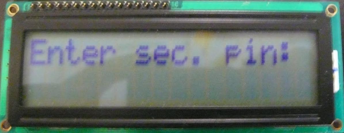
User Prompted to Enter Security Pin
The SendEthernetData state transfers (1) the amount, (2) the RFID tag and (3) the user-entered security pin over the Ethernet to a mySQL database that is queried for the received tag and checks if the security pin was entered correctly. If the tag is found, the security pin is correct, and the user has the given amount in his/her account a Good “G” signal is returned over the Ethernet. Else a Bad “B” signal is returned. The user is informed about the details of the transaction on the LCD. The actual implementation for Ethernet data transfer is explained in the “Ethernet” section of our report.
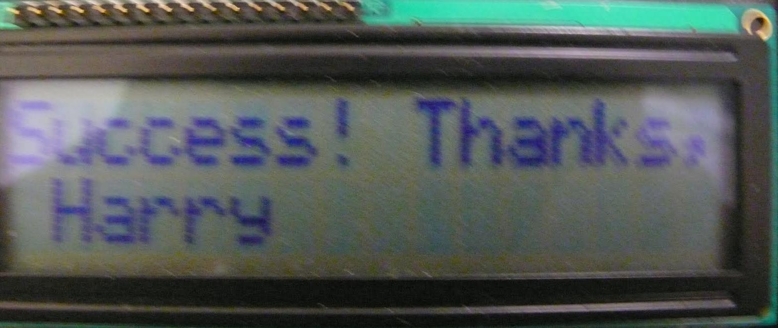
mySQL databsase returning a “Success” message, after identifying Harry's tag
A new transaction can now be started by pressing the reset button A, on the keypad.
Note: The LCD implementation was fairly straightforward because we had used the same LCD in previous labs and used the functions from the libraries that we were provided with. For a detailed explanation, please refer to the “LCD” section of our report. The keypad implementation was also done in a previous lab and hence we were fairly comfortable with both the circuitry and software required to include it in our final project. For a detailed explanation, please refer to the “Keypad” section of our report.
RFID
Before we start a detailed explanation of our implementation we will take a step back and talk a little about the technology in general.
Excerpts from the microID 125kHz RFID System Guide:
RFID Introduction:
Radio Frequency Identification (RFID) systems use radio frequency to identify, locate and track people, assets and animals. Passive RFID systems are composed of three components – a reader (interrogator), passive tag and host computer. The tag is composed of an antenna coil and a silicon chip that includes basic modulation circuitry and non-volatile memory. The tag is energized by a time-varying electromagnetic radio frequency (RF) wave that is transmitted by the reader. This RF signal is called a carrier signal. When the RF field passes through an antenna coil, there is an AC voltage generated across the coil. This voltage is rectified to result in a DC voltage for the device operation. The device becomes functional when the DC voltage reaches a certain level. The information stored in the device is transmitted back to the reader. This is often called backscattering. By detecting the backscattering signal, the information stored in the device can be fully identified.
RFID Tag:
Tag consists of a silicon device and antenna circuit. The purpose of the antenna circuit is to induce an energizing signal and to send a modulated RF signal. The read range of tag largely depends upon the antenna circuit and size. The antenna circuit of tag is made of LC resonant circuit or E-field dipole antenna, depending on the carrier frequency. The LC resonant circuit is used for the frequency of less than 100 MHz. In this frequency band, the communication between the reader and tag takes place with magnetic coupling between the two antennas through the magnetic field. The antenna utilizing the inductive coupling is often called magnetic dipole antenna. The antenna circuit must be designed such a way to maximize the magnetic coupling between them.
Modulation Protocol:
The passive RFID tag uses backscattering of the carrier frequency for sending data from the tag to reader. The amplitude of backscattering signal is modulated with modulation data of the tag device. The modulation data can be encoded in the form of ASK (NRZ or Manchester), FSK or PSK. Therefore, the modulation signal from the tag is Amplitude-Amplitude, Amplitude-FSK and Amplitude-PSK.
Carrier:
Carrier is the transmitting radio frequency of reader (interrogator). This RF carrier provides energy to the tag device, and is used to detect modulation data from the tag using backscattering. In read/write device, the carrier is also used to deliver interrogator’s command and data to the tag.
Frequency Shift Keying:
This form of modulation uses two different frequencies for data transfer; the most common FSK mode is FC/8/10 (FC is the carrier frequency). In other words, a ‘0’ is transmitted as an amplitude-modulated clock cycle with period corresponding to the carrier frequency divided by 8, and a ‘1’ is transmitted as an amplitude-modulated clock cycle period corresponding to the carrier frequency divided by 10. The amplitude modulation of the carrier thus switches from FC/8 to FC/10 corresponding to 0’s and 1’s in the bitstream, and the reader has only to count cycles between the peak-detected clock edges to decode the data. FSK allows for a simple reader design, provides very strong noise immunity, but suffers from a lower data rate than some other forms of data modulation.
Now, we were really lucky for a couple of reasons. (1) Cornell has had RFID tags embedded in each of the Cornell ID cards since Fall of 2003 so we could simply use these tags (albeit these tags would not be embedded in our cell-phones, this would be OK for now), (2) Craig and Ricardo (from Spring 2006) had already done all the research on Cornell’s RFID tags (we are extremely grateful to them for their comprehensive report).
Salient Points:
- The tags operated on a 125 [kHz] carrier frequency.
- The modulation method used was FSK (Frequency Shift Keying).
This information was extremely crucial because we saved a lot of time on research and could concentrate on building a robust system instead! Thus, now we knew that 0’s corresponded to a (125/8) 15.625[kHz] frequency and 1’s corresponded to a (125/10) 12.5[kHz] frequency.
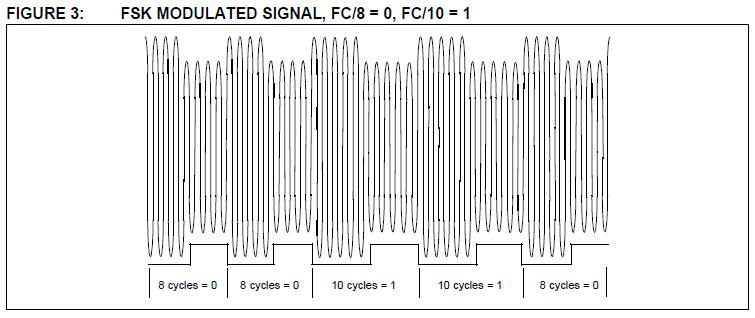
FSK Modulated Signal
Before delving into the specifics of the individual parts of the circuit here’s a breakdown of the top-level tasks (referenced from the microID 125kHz RFID System Guide):
-
Transmission: The transmitting section contains circuitry for a carrier signal (125 kHz), power amplifiers, and a tuned antenna coil. The 125 kHz carrier signal is typically generated by passing a 125 [kHz] square-wave signal from the Mega16 through an RF choke. The signal is amplified before it is fed into the antenna tuning circuit. A complementary power amplifier circuit is typically used to boost the transmitting signal level. An antenna impedance tuning circuit consisting of capacitors is used to maximize the signal level at the carrier frequency. This tuning circuit is also needed to form an exact LC resonant circuit for the carrier signal. The tuning compensates the variations in the component values and the perturbation of coil inductance due to environment effect.
-
Reception: The receiving section consists of an antenna coil, demodulator, filters, amplifiers, and microcontroller. The FSK reader needs two steps for a full recovery of the data. The first step is demodulating the backscattering signal, and the second step is detecting the frequency (or period) of the demodulation signal. The demodulation is accomplished by detecting the envelope of the carrier signal. A half-wave capacitor-filtered rectifier circuit is used for the demodulation process. A diode detects the peak voltage of the backscattering signal. The voltage is then fed into an RC charging/discharging circuit. The RC time constant must be small enough to allow the voltage across C to fall fast enough to keep in step with the envelope. However, the time constant must not be so small as to introduce excessive ripple. The demodulated signal must then pass through a filter and signal shaping circuit before it is fed to the microcontroller. The microcontroller performs data decoding after this.
RFID Hardware:
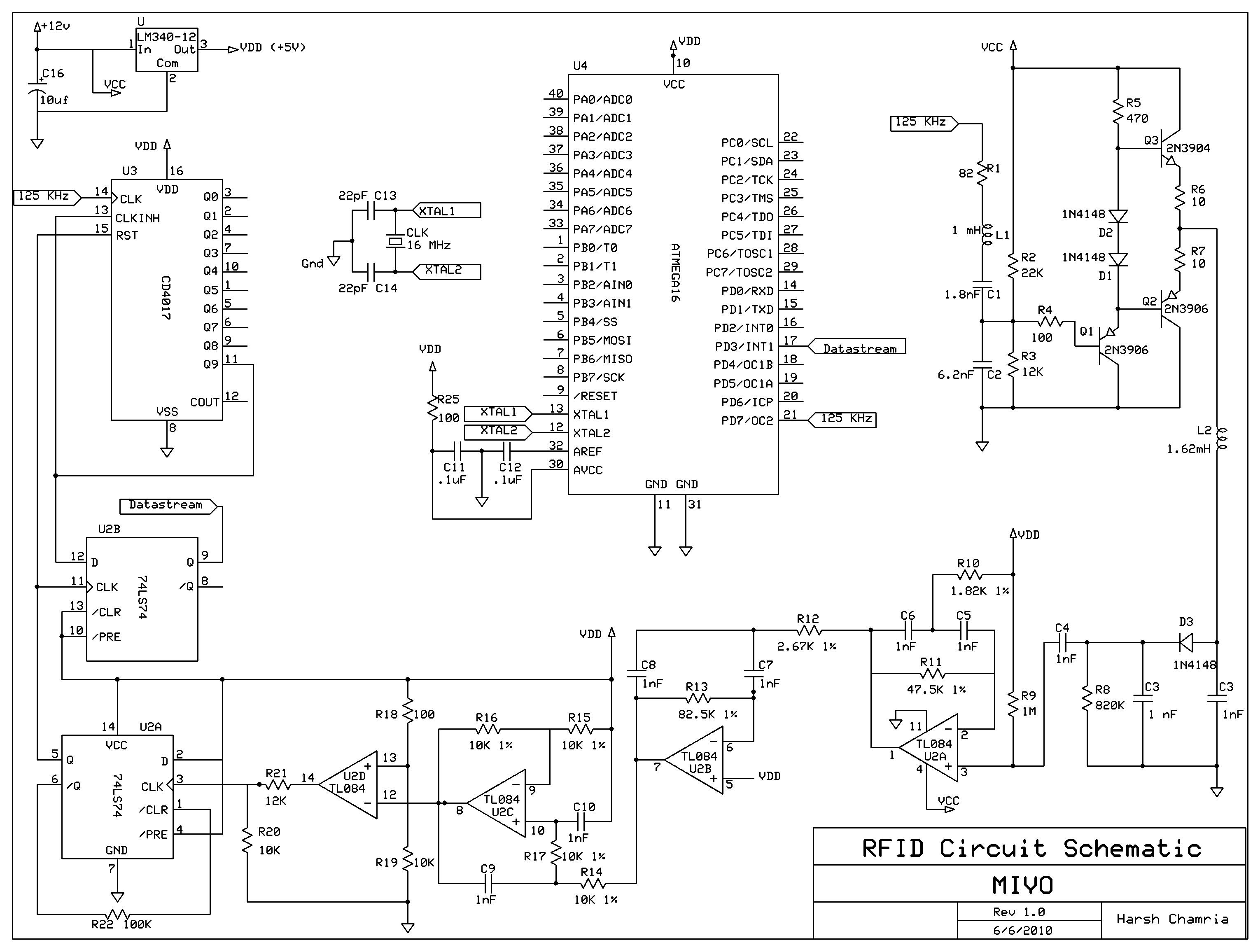
Complete RFID Circuit Schematic (Click Here for Full Size)
Note: We adopted the ATMega32 schematic from Spring 2008 as it fit in better with our design. However, the pin-configuration and external hardware setup are identical in the ATMega32 and ATMega16 chips.
Explanation:
Transmission- RF Choke and Power Amplifier: The circuit represents a 125 [kHz] square-wave signal fed into an RF choke followed by a current buffer and half-bridge amplifier.
The RF choke is used to filter majority of the high frequency signals in the square-wave, passing through only the fundamental harmonic (sine-wave) of 125 [kHz]. We could have generated a sine-wave in the MCU and passed that directly to the power amplifier however this would have been much more taxing on the MCU (as we would have had to implement a sine-wave table, etc). Generating a square-wave on the other hand is extremely simple and uses the MCU resources to a bare minimum (please see the RFID Software section for details). Diodes are used here, in order to remove crossover distortion (transients due to the half-bridge transistors switching between on and off states).
All of the components in this circuit were found in the ECE 4760 lab apart from the 1 [mH] inductor, which we ordered through DigiKey (part numbers can be found in the Parts List section).
Reception Antenna: This is definitely one of the most crucial elements of the circuit and we made sure to follow the recommendation (by the microID guide) of using a series L-C resonant circuit, as opposed to a parallel R-C circuit. This topology ensures that maximum current flow occurs at maximum resonance and also provides for a simpler design.
The resonance frequency is given by the equation:
![]()
As the ECE 4760 lab had 1nF capacitors in abundance, we decided to use C = 1 [nF]. This, along with (resonant frequency) f0 = 125 [kHz] gave us a value for L ≈ 1.62 [mH].
Now, for the construction of the antenna we decided to go for a rectangular shaped antenna as opposed to a circular one because from our preliminary end-product designs (i.e. aesthetic box) we knew that we would need a rectangular antenna. As far as the dimensions of this antenna are concerned, we decided that we would go with an antenna about the size of our whiteboard (as our box would have to be at least as large as the whiteboard (or solder board).
The [microID guide] came in handy here as well because we could simply use the equation for calculating the inductance of a coil. The equation for the inductance of an N-turn rectangular coil, with multilayer is:
![]()
Here: L- Inductance in [µH], {x,y}- {Length, Breadth} of coil in [cms], h- Height of coil in [cms], b- diameter of wire in [cms].
The values we used: L = 1620[µH], {x, y, h} = {4.2, 15.2, 1} [cms], b = 0.32[cms] (AWG28 lacquered copper wire from the ECE 4760 lab). Solving this equation for N gave us N ≈ 83 turns. Oscilloscope results below show the inductance coil output, both with and without RFID tags being present.
Reception Circuit: Since the capacitor (in series with the coil) is grounded, the carrier signal (125 kHz) is filtered out to ground after passing the antenna coil. The circuit provides minimum impedance at the resonance frequency. This results in maximizing the antenna current, and therefore, the magnetic field strength is maximized.
We now need to half-wave rectify and R-C filter the received signal. The inductor, capacitor and diode (and the other bottom parts in the circuit) form a signal receiving section. The voltage drop in the antenna coil is a summation (superposition) of the transmitting signal and backscattering signal. The diode is a demodulator which detects the envelope of the backscattering signal. The diode and capacitor (2.2nF) form a half-wave capacitor-filtered rectifier circuit. The detected envelope signal is charged into the 2.2nF capacitor. The resistor provides a discharge path for the voltage charged in the capacitor. This voltage passes active filters and the pulse shaping circuitry. Finally this signal is passed through a capacitor (1nF) which knocks off the DC offset.
Filtering Circuit: Next we use active Twin-T and Butterworth filters using the TL084CN (high-speed) Op Amp. The first filter acts as an isolator with bandwidth being 10[Hz] – 20[Hz], and unity-gain for all frequencies outside the band. The second filter introduces some more gain into the pass-band. Next, the signal goes into a Butterworth filter with sharp roll-off. This filter gets rid of any high-frequency components in the signal.
Finally, the filtered signal is passed through a comparator to generate a square-wave type signal. The final result is that we get very clean 12.5[kHz] and 15.625[kHz] frequencies out of the system.
One of the major differences in our design from the previous year’s design was that we got no signal when a tag was not present near the coil. This is great because we didn’t need any hack to ignore this signal.
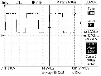
Oscilloscope outputs from comparator (12.5[kHz])
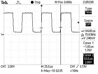
Oscilloscope outputs from comparator (15.625[kHz])
Note: We did not simulate any of these circuits simply because we were using a commercial guide (presumably thoroughly tested) and we were lucky to have the Sp 2006 group’s simulation results. In fact, we devoted our time to trying out different values of components in order to achieve the best performance. For further details (such as how to increase the range, etc, please refer to the microID 125kHz RFID System Guide).
Hardware/Software Tradeoff & Data Creation: We debated whether we could take the filtered signals and feed them directly to the MCU or if we would need some more hardware decoding. However, in order to accurately measure the frequency of the incoming data we would have to sample at a rate of about 125[kHz] and this would take up a lot of the resources of the MCU (at a clock rate of 16[MHz] this would give us 128 cycles to do everything else). We realized this because Craig and Ricardo had explained this pretty well in their report and also because we knew that it would be much faster to do this in hardware. Now, the microID RFID guide provided a really smart way that made use of D flip flops and a decade counter. The circuit is designed as follows:
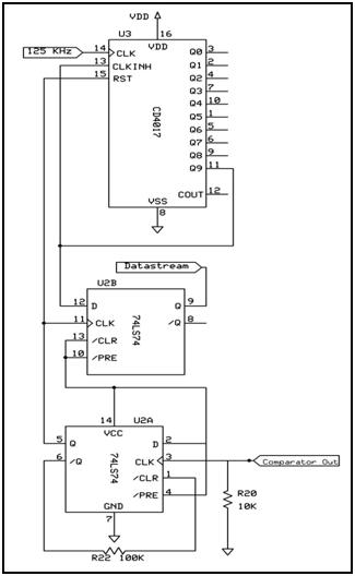
Digital Component of RFID Circuit
(Click Here for Full Size)
The explanation for this circuit is taken from Craig and Ricardos webpage as they did a great job of documenting and explaining the logic: The comparator output serves as the clock for the first D flip-flop, which also takes logic 1 as its D value. On the rising edge of the comparator clock, Q is immediately set to 1. However, simultaneously ~Q goes low and clears the flip-flop. This creates an extremely short pulse which serves as a reset for the decade counter and clock for the second flip-flop. The decade counter is just a 1-hot counter which takes a 125 KHz clock. With every rising edge of this clock, the counter outputs the next pin to logic 1; so typical output would look like (if one were looking at output pins 0-9 of the counter) 1000000000 0100000000 00100000000 etc. However, this counter is being reset with every rising edge of the comparator output. Thus, since we've already determined that 125 KHz/10 = 12.5 KHz is to be our frequency that represents logical 1, all we have to do is check for the output on pin9 to know whether or not we see that frequency. If the system is operating at either one of the other possible frequencies, the counter will be reset before pin9 can go active. The pin9 output serves as input to the second flip-flop and also to the clock inhibitor, which keeps the 9th pin high until the counter is reset. Because of this set-up, the Q output of the second flip-flop will remain logical 1 so long as modulating frequency is 12.5 KHz and will drop down to 0 if its anything else. Theoretically, this circuit should work perfectly. However, experimentally it did not, and thus required a small modification. The 100 KOhm resistor on the first flip-flop serves to lengthen the time it takes for the ~Q signal to get to CLEAR. Since all transistors have some amount of natural capacitance, this forms an RC circuit of sorts with a set RC time constant for the signal to rise or fall. As it turns out, this time was too short for the decade counter. The original design from the reference guide specified only a 10KOhm resistor between ~Q and CLEAR. With the 10[KOhm] resistor, pulse widths for the reset pulse were a mere 50 [ns] long, while the counter required at least 250 [ns]. This caused some very erratic behavior. After many hours of debugging, we finally pinpointed the problem and replaced the resistor with the 100 [KOhm] resistor which increased the pulse width long enough for the counter to correctly operate.
RFID Software: Once the data was converted into a digital Manchester signal by the RFID circuit, we then had to process it and convert it into a useful format to the microcontroller. For this, we decided to write a library for the RFID, called rfid.c, which dealt specifically with the task of receiving and interpreting an RFID signal. Unlike Ricardo and Craigs design for RFID, we did not use a sampling method for Manchester decoding. Instead, we opted for a more robust method with less interrupts a timing-based method. This method only interrupts when it has to i.e. on a change of logic value, and then the microcontroller interprets the amount of time between interrupts in order to determine the value of the Manchester bit. To do this, we go through a sequence of events after turning on the external interrupt for any logic change:
- Wait until we receive a start sequence (extra long logic high)
- On next interrupt, decode the first Manchester bit: delay by a very short amount to ensure steady state, read the logic level.
- If time difference is short, save the read logic level into a data buffer only if it wasnt recorded last time. If time difference is long, save the logic level.
- If anything was recorded in the previous step, add to the checksum such that it is sample number dependent (we used sample * i % 9, where i is the sample number)
- Repeat steps 2 and 3 until we read an end sequence (extra long logic low)
- Insert a 2 at the end of the buffer, so we know where we stopped recording
The sample number dependent checksum was added as a feature since it is more likely to be wrong in the case of multiple bit errors. If we only added the binary values, we would have created a parity check, which may not have been sufficient in cases of a lot of noise. This allowed us to cut down on the number of redundancy checks by a factor of three, and still get the same reliable results, leading to a faster system. To better explain what we mean by short, long, and extra long: since Manchester encoding has a logic change at every data bit, the longest delay we could have would be 0110. That means that during the pair of 1s, it stays logic high for two half-cycles. The shortest delay we could have would be 0101, where the 1 stays high for only one half-cycle. For the RFID system, if we clock it at the same scale as the previous two, there is also another state, which is 111110. This is a very long time, easily detectable, and denotes the start of a data stream. Once we successfully fill the buffer, we ensure the reliability by checking it multiple times. We checked 20 times, which was way overkill, but we really wanted to minimize the chance of a wrong ID. In reality, two checks actually is sufficient for most of the time, with three checks delivering near perfect results. Since we are only reading a 44-bit value from the RFID tag, we can do the 20 checks very quickly (approximately one second in most cases). We saved each data bit as a char in a string, so then we just convert it into a long using bin2dec so it can be returned using less space than a string. One cool final note was that by doing Manchester decoding with the timing-based method, we were able to get the data by only connecting one wire for ground and one wire for data to the microcontroller!
Manchester Encoding [from Wikipedia]:
In telecommunications, Manchester code is a line code in which the encoding of each data bit has at least one transition and occupies the same time. It therefore has no DC component, and is self-clocking, which means that it may be inductively or capacitively coupled, and that a clock signal can be recovered from the encoded data. Essentially Manchester encoding works in the following way: A transition from 0 to 1 corresponds to a single 1 value and a transition from 1 to 0 corresponds to a single 0 value. Thus 01 -> 1, 10 -> 0, and the reduced bitstream is half as long as the original bitstream.
Ethernet
Hardware Overview:
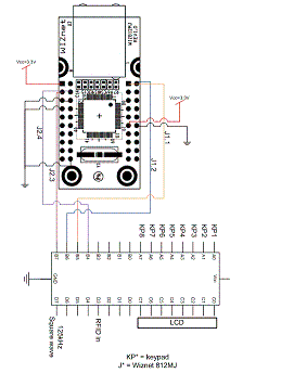
Master Hardware Circuit Schematic (Click Here for Full Size)
Ethernet Background:
Ethernet is the term encompassing the primarily wire-based network protocols and specifications in use throughout the world today. It was originally developed in the early 1970s by Xerox PARC in order to facilitate the development of large computer networks. Ethernet uses a packet-frame architecture to transmit data (namely IP), and has methods available to deal with network congestion and reliable transport. Specifically, the pieces of the Ethernet that we used directly were: cat5 twisted-pair cabling, TCP (Transmission Control Protocol), MAC (Media Access Control), IP (Internet Protocol), HTTP (Hypertext Transport Protocol).
Connecting these Ethernet devices together physically is twisted-pair cat5e cabling. We used 100BASE-TX speed, which can transmit up to 100Mb/s over the line. This IEEE 802.3u standard provides an efficient physical connection layer utilizing (not surprisingly) twisted pairs of cable to transmit bits. Clients receiving or transmitting using 100BASE-TX are responsible for synchronization and encoding bits into ‘4B5B’ binary encoding.
In IP, each device gets an IP address that uniquely identifies itself to the local network. This number is a 32-bit integer, usually organized into 4 bytes separated by periods, for example x.x.x.x, where x represents a 0-255 number. What is called a subnet mask also exists, which creates a bitmask which determines which bits must be fixed during communication.A typical subnet mask might be 255.255.255.0 (corresponding to 0xFF.0xFF.0xFF.0x00), meaning that the device can only connect to other devices with address x.x.x.y, where y can be anything from0-255.
Additionally, for device to device communication in IP, each device needs to have a MAC address. This 48-bit number (every byte delimited by a ‘:’) is a unique identifier for each Ethernet interface, and IP uses it so that packets can find their way to the destination. A MAC address can be considered like a ‘Social Security Number’ of a networked device. An example MAC address might be: 48:32:AE:4B:18:F6.
Running on top of IP, we used TCP to provide reliable data transfer. This protocol, which is designed to maintain connection state, encapsulates its underlying data with a TCP header of 20-60 bytes, which provides all of the information necessary for reliable transmission and congestion control. Aside from this, we will leave it to the reader to research, since TCP is very well documented elsewhere and not a significant portion of our project.
Finally, the most visible method of communicating over Ethernet is via HTTP. Once we are at the point that we can take the underlying levels previously described for granted, we can transmit data. HTTP is the incredibly ubiquitous protocol used in the World Wide Web today, and specifies methods of requesting and receiving text from an IP address. HTTP uses a header format that looks like:
GET /process.php?rfid=491829822&pin=1234&amt=30 HTTP/1.1
Host: 10.0.0.100
As you can see, HTTP headers can be relatively simple. In reality, though, a typical web page request uses many more optional parameters that give extra information to the server, but this is beyond the scope of our project. In order to pass context information to the server, which would allow it to display dynamic content, HTTP specifies two methods: GET and POST. The latter essentially codes variables, hidden to the user, as part of the HTTP data, while the former simply appends the variable names and values to the end of the URL, using a format such as seen in the diagram.
Our Implementation:
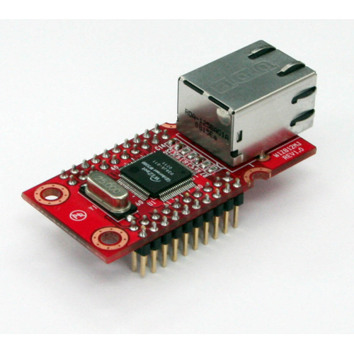
Our Ethernet Chip: WIZ812MJ
Luckily for us, we were able to get our hands on a Wiznet WIZ812MJ Ethernet development board, which abstracted the design for every layer except HTTP. The WIZ812MJ board gave us pins and a physical Ethernet port, which was actually connected to a Wiznet W5100 chip, which did the actual network processing. So, instead of actually coding the complex state machines associated with each protocol, the W5100 chip did that for us, and we just had to communicate with it via SPI (Serial Peripheral Interface).
Communicating over HTTP:
For our application, we sent HTTP ‘GET’ requests, with our parameters encoded as GET variables. First, we had to create a library for interfacing with the W5100, which we called ‘ethlib.c’. This library was created with a base from Brian Bryce’s AVR POP3 mail fetcher, which also used the W5100. In essence, this library provided the framework for setting up and connecting to an Ethernet network. All of the code was modularized and parts that were unnecessary to us were stripped so that it could be executed from another program, and some additional features were added. In addition, Bryce’s code had some connection reliability problems that were diagnosed, debugged, and fixed in the final library. Some of the features we added was a ‘connect_defaultTCP’ method, which just connected the device to predefined parameters. This helped clean up the code a lot, and also made it easy to change the parameters. We decided against using the EEPROM storage available on the ATMega16 for network parameter storage as Bryce did. This design decision was simply because we had enough space to commit them to data memory, and we did not want to add a whole set of functions dedicated to setting up the device from EEPROM. That said, a lot of time was still spent debugging and documenting the W5100 until we were satisfied we had an extremely reliable device and connection established. We used 10.0.0.100 as the IP address of the server, and 10.0.0.101 as the IP address of the W5100.
For HTTP communication, since the W5100 reports the entire HTTP response back (including the header), we needed a way of parsing out the data. The communication standard we designed had the actual data stream start with a “$” character, and end with a “^” character. This allowed us to efficiently discard the HTTP response header in C code, so that we would be left with the data. The authentication response was also encoded in a specific format: if the authentication was not successful, we returned a status code of ‘0’, followed by nothing else. If the authentication was successful, but the user did not have sufficient funds for the transaction, we denoted this with status code ‘1’, followed by the user’s name. If everything went well, and the transaction succeeded, we return status code ‘2’, followed by the user’s name. An example success, for example, looked like: “$2Harry^”.
Ethernet Backend Operations:
From the point when we had the Ethernet library and a data transfer protocol established, all that was left was to use it to transmit the data we collected from our user to the server. As previously stated, we did this by encoding the data as GET variables: ‘rfid’, ‘pin’, and ‘amt’. ‘rfid’ corresponds to the RFID value, converted to a long, read in from the RFID method. ‘pin’ corresponds to the entered pin number, and ‘amt’ corresponds to the entered payment amount. This data was passed to a PHP script, process.php, which was running on a LAMP (Linux, Apache2, Mysql, PHP) server. The process.php script’s purpose was two-fold: authenticating the user and replying with the appropriate status code and authentication data, and also to log every attempt made to access the system. We made sure to output something every time process.php was accessed – authentication and payment successes were logged to the ‘rfid.log’ file, and anything else was logged to ‘fail.log’, along with the reason for failure. In addition, if there was a successful transaction, we also logged the information about the transaction into the database, in a specific table called ‘transactions’. This presents users with a way to view their transaction history. Once all has been logged, and the response sent, the microcontroller then parses the response and displays an appropriate message to the user.
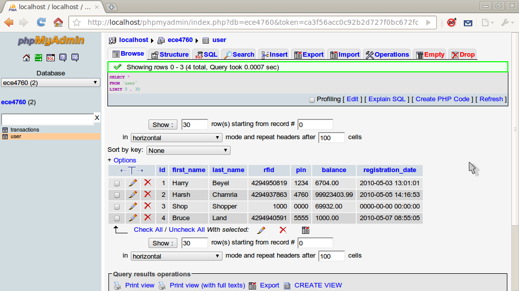
User Database Snapshot(Click Here for Full Size)
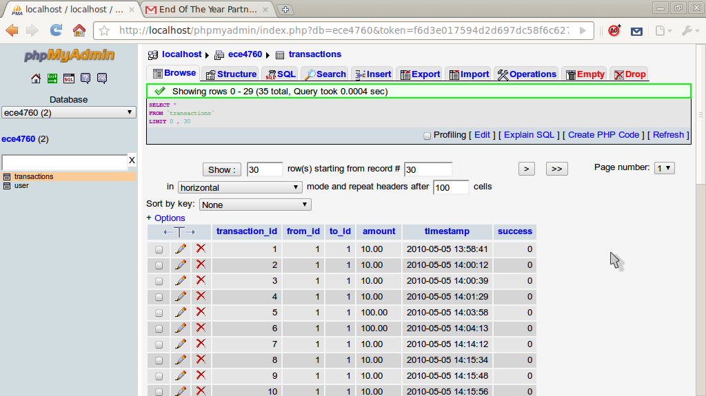
User Transaction Snapshot(Click Here for Full Size)
Ethernet Pin Configuration:
| J1 | J2 |
| 1 -> B.5 | 1 -> VCC |
| 2 -> B.6 | 3 -> B.7 |
| 11 -> GND | 4 -> B.4 |
| 12 -> VCC | 5 -> GND |
| 6 -> GND | |
| 7 -> GND | |
| 20 -> GND |
LCD:
We decided to use a 16x2 LCD as it was readily available in the ECE 4760 lab. We had used the LCD in multiple labs previously and the documentation for the LCD can be found here. Information on how to connect the LCD and code to test the connections can be found in the Spring 2010, ECE 4760, Lab 1 page here.
Keypad:
We needed a keypad that had all the decimal digits (i.e. 0-9) and a couple of extra keys for “Reset” and “Cancel” functions. We decided to use the 4x4 keypad as it was easily available in the ECE 4760 lab. We connected Pins 1-8 on the keypad to Port A pins A.0-A.7. More information on wiring for the keypad and the code to test the connections can be found in the Spring 2010, ECE 4760, Lab 2 page here.
Microcontroller Operations:
We decided to use the Atmel Mega 16 microcontroller (as opposed to the Mega 644 that we had used in all of our labs during the semester) simply because we did not need much on-chip memory and the Mega 16 would count as a “free” chip in our budget (of course, we were also comfortably under-budget). We would like to extend our gratitude to Professor Land for providing us with his excellently designed MCU board. We used the Max233CPP for the RS232 connection during the debugging phases, but did not need it in the final project demonstration. The documentation for this board can be found here.
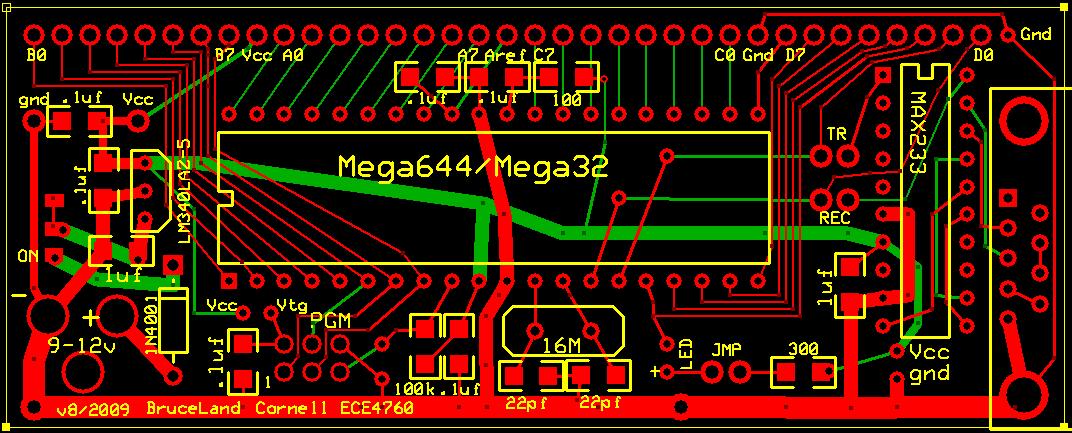
Prototpe Board Schematic (Credit Prof. Land)
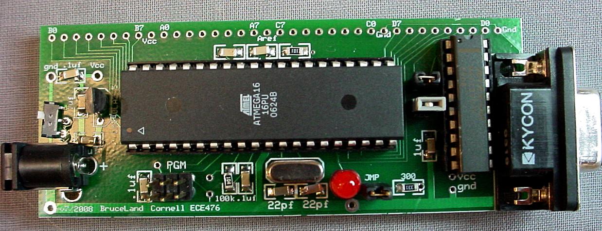
Completed Prototpe Board Circuit (Credit Prof. Land)
Port/Pin Configuration on MCU:
Pin D.7 - 125[kHz] square wave to generate the RFID carrier frequency.
Pin D.3 - External Interrupt 1 to accept filtered data from the RFID reception circuit.
Port A - Keypad (Pins [1-8] on keypad correspond to Pins [A.0-A.7]).
Port C - LCD (please refer to the “LCD” section of the report for the setup).
Pins [B.4 - B.7] - Ethernet (please refer to the “Ethernet” section of the report for the setup).
Standards:
ISO/IEC 14443 or ISO/IEC 15693:
The Cornell ID cards we use in this project are developed by HID®. Specifically, the Cornell ID is a HID DuoProx II card that is also ISO 7810 compliant (magnetic strip). We did not need to use the magnetic strip feature. The card is also ISO/IEC 15693 compliant; ISO 15693 was developed in 1999 and has become the standard for contactless payment systems.
ISO/IEC 18000:
This is an international standard that describes a series of different RFID technologies. We use ISO 18000-2, which describes the air interface communications below 135 [kHz].
TCP/IP [taken from Wikipedia]:
The Internet Protocol Suite (commonly known as TCP/IP) is the set of communications protocols used for the Internet and other similar networks. It is named from two of the most important protocols in it: the Transmission Control Protocol (TCP) and the Internet Protocol (IP), which were the first two networking protocols defined in this standard. Today's IP networking represents a synthesis of several developments that began to evolve in the 1960s and 1970s, namely the Internet and LANs (Local Area Networks), which emerged in the mid- to late-1980s, together with the advent of the World Wide Web in the early 1990s.
Ethernet [taken from Wikipedia]:
Ethernet is a family of frame-based computer networking technologies for local area networks (LANs). It defines a number of wiring and signaling standards for the Physical Layer of the OSI networking model as well as a common addressing format and Media Access Control at the Data Link Layer. Ethernet is standardized as IEEE 802.3. The combination of the twisted pair versions of Ethernet for connecting end systems to the network, along with the fiber optic versions for site backbones, is the most widespread wired LAN technology.
mySQL [taken from Wikipedia]:
MySQL is a relational database management system (RDBMS)[1] that runs as a server providing multi-user access to a number of databases.
Results
Speed of Execution:
Our mobile-payment system prototype completed read an RFID tag in about a second, and database access over Ethernet took less than 1 second. In all, the user would be strictly “waiting” only for a total of about 2 seconds. Of course, this 2 seconds does not take into account the time that the cashier takes to enter the amount, or the time that the user takes to enter his/her security pin. In order to make the RFID reading quicker we would need to reduce the number of times we check the tag. We did not want to reduce the number of checks from 20 to say 5, but that would also reduce the accuracy of the system.
Accuracy:
We had an accuracy of 100%. We had no false positives, as we would check the same tag 20 times in order to make sure that the ID is actually the same. However, depending on the angle in which the tag is held in front of the coil, or the distance of the angle from the coil, we did have a few false negatives. Now, we could account for this in software but we can’t find any hardware method to detect this scenario. In the eventual commercial application, when the tag is used a sticker on the user’s phone, users could simply be prompted to bring their phone within a 1” reading distance.
Safety:
This device does not pose any safety or health threats to its users. We have an insulating card-board box as the container for the system and the user interacts with the device only through the keypad, which is made out of insulating plastic. There are power and Ethernet cables that are connected to the device and these components cannot inflict harm upon a user as the user does not interact with these cables.
Interference:
This is an issue that any communication medium deals with, however, as this is a “Near-Field-Communication” system, chances of interference from another 125[kHz] emitter are very slim. Also, if there are two tags on a user’s phone (say for different applications, both using 125[kHz] as the carrier frequency), the system would be unusable. However, in the general case, this system does not suffer from any interference issues.
Usability:
Our system is usable by most individuals without serious physical ailments. Individuals with certain disabilities may find our device inconvenient to use, however we are in no ways discriminating against anyone. The device may be modified so as to offer auditory feedback for the blind, Braille key-modification on the keypad and possibly voice recognition for authentication for individuals who have lost their hands.
Conclusions
We feel that we have successfully implemented the first prototype of our mobile-payment system. We achieved every goal that we had defined in our Project Proposal and at the end of a fantastic five weeks we are extremely satisfied with our mammoth project! We will be looking forward to adding all our friends to our database and stress-testing the system to iron out any creases. Our next step will be to implement data transfer over a 2G network, after which, we will be aim to add levels of encryption to make the system hack-proof.
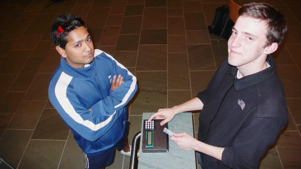
Relief, Satisfaction, Happiness!
Ethical Considerations:
We ensured that our project properly follows the IEEE Code of Ethics and our project does not pose any ethical problems. We believe that all the decisions we made were fully ethical and followed the code of ethics guidelines. While working in lab we ensured that we met with the highest safety and health standards, and made sure that we were not adversely affecting the welfare of the public. Moreover, this device does not pose any safety or health threats to its users. We have an insulating card-board box as the container for the system and the user interacts with the device only through the keypad, which is made out of insulating plastic. There are power and Ethernet cables that are connected to the device and these components cannot inflict harm upon a user as the user does not interact with these cables.
While developing this project we did not come across any situations that involved perceived conflicts of interest. In fact, as is expected in the ECE 4760 lab we were always willing to help our fellow classmates whenever they asked for assistance in their projects. To our knowledge we have been fully honest in making any claims or stating any estimates based on measured data. There was never any instance of bribery that we encountered. Also, as we have mentioned before, neither of us were experts in the fields of the various components we used in our project, and our goal was to improve the understanding of technology, it’s potential applications and eventual consequences. We hoped to use existing technologies to develop a device that can truly serve as a proof-of-concept for a mobile-payment system. We had intended to maintain and improve our technical competence and understand that we can undertake technological tasks for others only if we are qualified by training, or after the full disclosure of pertinent limitations.
We are open to advice, criticism and essentially any comments on our technical work. We will be willing to acknowledge and pleased to correct any errors, and have made sure to credit properly the contributions of others. Our device does not discriminate against any race, religion, gender, age or national origin. Individuals with certain disabilities may find our device inconvenient to use, however we are in no ways discriminating against anyone. The device may be modified so as to offer auditory feedback for the blind, Braille key-modification on the keypad and possibly voice recognition for authentication for individuals who have lost their hands. During the course of our project, we made sure to avoid injuring any fellow classmates, their property or reputation by malicious action. On the contrary, we were always glad to help our classmates out whenever we could be of assistance.
Intellectual Property Considerations:
As mentioned before, neither my partner nor I have taken courses in RFID design and in fact this was our first experience in working with the standard. We have made sure to cite any and all designs that we referenced (in our “Acknowledgements” section) and locally while describing the module. There are many patents filed by the HID corporation itself on methods to read their cards (an example can be found here. Similarly there are many patents filed under mobile payments (an example can be found here. However, we have violated no patents while working on our project as (1) we have a specific concept for our final system (and this prototype is just the first step in getting there), (2) this is an academic project that is following all FCC standards .
We are very grateful to WIZNET for sampling us their WIZ812MJ module. They did not require us to sign any non-disclosure as no code came with the device.
Legal Considerations:
[From RFID Gazette] Part 15 of the FCC’s rules for low-powered devices deals with RFID regulations. RFID devices are referred to as “intentional radiators”. These low-powered devices do not raise a serious threat of interference with other devices and hence can be operated without a license. All the same, RFID devices have to meet the RF emissions limitations and power restrictions as laid down by the FCC.
Societal Impact:
As Internet and ATM machines are unavailable in rural areas and penetration is low even in urban areas, the following problems exist:
- Individuals who have opened bank accounts in the cities have a problem accessing their bank-services
- Individuals without bank-accounts who would like to avail of convenient services such as ATM debit cards have to resort to cash for all their financial needs
- Migrants working in places elsewhere in the country have difficulties sending their remittances home
- Financial institutions find it unviable to setup station in remote locations in the country
- Micro-finance lenders have trouble connecting with viable recipients
- Average Revenues Per User and margins for telecomm operators have been declining and the field needs Value Added Services if it is to sustain healthy growth
An idea such as Mivo has the potential to solve these issues. We see many problems in today’s payment systems in developed countries- security and convenience (of say, peer-to-peer payments) being the important ones. No system is perfect but the system we envision could potentially solve these issues.
Acknowledgements:
First and foremost we would like to extend our gratitude to Professor Bruce Land for preparing us to develop our Final Project through the course of the semester, have the lab open endless hours for our projects and for helping us debug our problems. We want to thank Bruce for his code for the LCD libraries.
We would also like to thank all the TAs for all their help and particularly our Friday lab TA, Yuchen Zhang.
We are extremely grateful to WIZNET for donating us their WIZ812MJ module. We would recommend any future ECE 4760 students to approach WIZNET for their networking considerations!
Finally, we are grateful to Craig Ross and Ricardo Goto (Spring 2006), whose comprehensive report made it possible for us to complete our project in the given time, even though we had so many varied components to integrate into a single microcontroller chip. Their project can be found at: http://instruct1.cit.cornell.edu/courses/ee476/FinalProjects/s2006/cjr37/Website/index.htm. We found the microID 125[kHz] reference guide through them which turned out to be the most helpful resource. The datasheet can be found at: http://ww1.microchip.com/downloads/en/DeviceDoc/51115F.pdf.
We would also like to thank Brian A. Bryce for his Ethernet code. Brian wrote POP3 Email client using W5100 and his code can be found at: http://babryce.com/w5100/emailV010.c. It is quite a co-incidence that Brian is actually a Cornell alumni (we found out from his stellar CV).
Division of Work:
| Harsh | Harry |
| RFID Circuit | RFID Receive Code |
| RFID Transmit Code | Ethernet Code |
| State Machine Code | State Machine Code |
| System Integration | System Integration |
| Final Report | Final Report |
| Website Design | |
Appendix
Parts List
| Part | Manufacturer/ Supplier | DigiKey Part Number | Unit Cost | Quantity | Total |
|---|---|---|---|---|---|
| RF Choke | JW Miller A Bourns Company | 5800-102-RC | $1.33 | 1 | $1.33 |
| Op Amp | Texas Instruments | TL084CN | $0.63 | 1 | $0.63 |
| Decade Counter | Texas Instruments | CD4017BE | $0.50 | 1 | $0.50 |
| Dual D Flip Flop | ECE 4760 Lab | SN74HC74N | $0.00 | 1 | $0.00 |
| Diodes | ECE 4760 Lab | 1N4001 | $0.00 | 1 | $0.00 |
| Transistors | ECE 4760 Lab | 2N3906. 2N3904 | $0.00 | 2 | $0.00 |
| Ethernet Controller | WIZNET | WIZ812MJ | $0.00 | 1 | $0.00 |
| LCD | ECE 4760 Lab | - | $8.00 | 1 | $8.00 |
| Keypad | ECE 4760 Lab | - | $6.00 | 1 | $6.00 |
| Breadoard | ECE 4760 Lab | - | $6.00 | 1 | $6.00 |
| Power Supply | ECE 4760 Lab | - | $5.00 | 1 | $5.00 |
| Custom PC Board | ECE 4760 Lab | - | $4.00 | 1 | $4.00 |
| Mega16 | ECE 4760 Lab | - | $0.00 | 1 | $0.00 |
| DIP sockets | ECE 4760 Lab | - | $0.50 | 2 | $1.00 |
| Header Pins | ECE 4760 Lab | - | $0.05 | 60 | $3.00 |
| Misc: Caps/ Resistors/ Regulators | ECE 4760 Lab | - | $0.00 | 1 | $0.00 |
| Total | $35.46 |
Code Listings:
Main Program Files:
state_machine.c
ethlib.c
rfid.c
HTTP Backend Files:
eth_setup_476.sh
mysql_close.inc.php
mysql_connect.inc.php
process.php
Libary and Header Files:
ethlib.h
rfid.h
lcd_lib.c
lcd_lib.h
uart.c
uart.h
References
MicroID 125[kHz] Reference Guide
Ricardo and Craig’s website
Bryan Bryce’s website
WIZ812MJ datasheet
ATMega16 datasheet
Related Resources
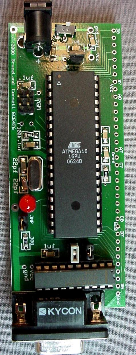
Protoboard with Atmel Mega 16. This brings our project together.
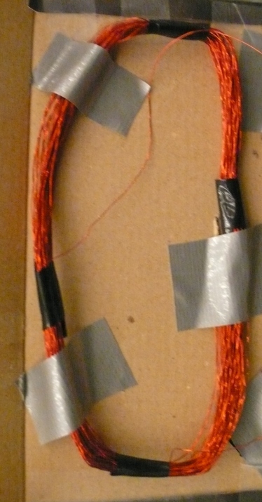
Our RFID Antenna - made of lacquered copper wire
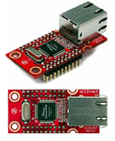
WIZ812MJ - connects our system to the Internet
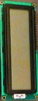
Our 2-Line 16-Character LCD
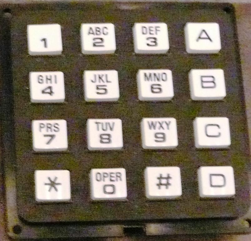
Our 4x4 Keypad
![125[khz] Carrier Wave](images/photos/125kHz_square_wave.jpg)
Our 125[kHz] carrier wave (Click Here for Full Size)
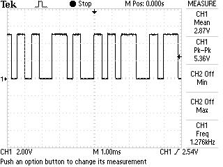
RFID tag datastream to MCU (Click Here for Full Size)
