ECE4760 Final Project:
Compact Guitar Pedalboard
Spring 2011
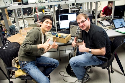
Brian Choi (bmc68), Michael Kilzer (mjk277)
Logical Structure
The implementation of the pedalboard is fairly straightforward. The input audio signal will first be equalized and amplified with an op-amp-based circuit. This signal will be converted into a 16 bit digital value through an external analog-to-digital converter, and then sent to the microcontroller for digital signal processing. User input will be used to control the parameters of the digital effects (whether they are on/off, effect strength). The microcontroller will take the digital input data, process the necessary effects, and output the processed signal through an external digital-to-analog converter. The DAC will convert the digital signal to an analog signal that can be played by a speaker or an amplifier. The microcontroller will also provide some feedback through status LEDs which will indicate the effects that are currently active.
Effects Summary
Volume
Often it is important for the volume to be adjusted when playing guitar, especially in situations such as before and after solos. The volume effect will adjust the gain of the audio signal, resulting in a louder or softer sound. The volume effect is controlled by a slider which the user can adjust to modify the gain.
Equalizer
The equalizer is used to modify the gain of specific frequency regions. For the guitar, this unit is used to enhance or emphasize certain aspects of the guitar’s tone, such as the low midrange regions (giving a warmer sound) or the treble regions (giving a brighter sound). The equalizer has six bands, with pass-band frequencies centered around 100, 200, 400, 800, 1600, and 3200 Hz. The equalizer, like the volume unit, is also controller by sliders which can be used to adjust the gain for each band.
Overdrive/Distortion
There are two different settings to this effect; both have different implementations. The user can toggle through the settings by stepping on the overdrive switch. Overdrive, otherwise known as “soft” clipping, will attenuate signals based on the level of the signals. This means that the signal peaks will be attenuated while the rest of the signal is left relatively unchanged. The result is additional overtones, which generate a warmer sound. The second setting, which is distortion or “hard” clipping, will clip the signal if it is higher than a set threshold. This results in a “dirty”, gritty sound.
Compressor
This effect is one of the least noticeable by listeners, but it is invaluable to guitarists. This effect will be activated by the compressor switch. This effect will lower the dynamic range of the signal, by increasing the gain of low amplitude signals and decreasing the gain of high amplitude signals. As a result, the resulting sound will be relatively at the same volume, no matter how loud or soft one may be playing. Compression also has the effect of sustaining the guitar sound, meaning that the sound will “ring” longer than usual after a note has been played.
Chorus
This effect applies slight variations in pitch to part of the audio signal, and recombines the processed signal with the original signal. The result imitates the effect that is produced by choirs and orchestras, where the sound seems like it has been produced by many instruments. This effect is activated by the stepping on the appropriate switch. Also, the amount of the signal that is modified can be altered by turning a knob.
Hardware/Software Tradeoffs
Use of external ADC
In the implementation of our project, a decision had to be made regarding whether the internal ADC on the Mega644 should be used or an external ADC should be used. In favor of the internal ADC, it would be quite simple to implement, requiring only a few bits in the ADCSRA and ADMUX registers. On the downside though, the ADC on the MCU would only be capable on 10-bit resolution at a maximum which is not very good for audio reproduction. This was confirmed when we hooked up the guitar to the internal ADC and heard a very noisy signal.
The external ADC (Analog Devices AD7680) had a 16-bit resolution which would be quite adequate for our purposes. Furthermore, the ADC used SPI to interface with the microcontroller, making it easy to communicate data from the ADC to the MCU. While not as easy as the internal ADC to use, SPI is an intuitive protocol, which made the code implementation of reading in data straightforward. When we tested the external ADC with the guitar, the results were much better as a cleaner sound was heard. For the ADC, the hardware won over the software method as it could read in a higher resolution.
Use of external DAC
The same train of thought that went into choosing to use an external ADC went into choosing to use an external DAC. Our goal was to maximize the output resolution. The resolution we would be able to achieve via PWM would be 8-bits maximum. Using Pulse Width Modulation as a DAC is an elegant solution. However, using the PWM would mean that we would waste the extra bits of resolution provided to us by the AD7680. Through the use of an external DAC (Linear Technologies LTC1657) we were able to preserve the 16 bits of data we read in with the ADC. The ability to have a finer resolution in the DAC enabled us to further nuance our effects more than we would have been able to otherwise with PWM.
Use of analog filters
In choosing between a software-implemented equalizer and a hardware-implemented equalizer, the decision was based upon three criteria: 1. Does it add complexity to the code? 2. Is the sound quality preserved? 3. Is it hard to implement hardware-wise? For the hardware implementation of the equalizer and filters, it does not add any complexity to the code and preserves the quality of the input audio quite well. The implementation while not hard is quite tedious due to the amounts of soldering and wiring involved. The software implementation does add complexity to the software while preserving the quality of the input audio thanks to the 16 bit ADC and DAC. The hardware would also be easier to manage since the potentiometers needed would simply be attached to the microcontroller rather than the filter circuitry with additional operational amplifiers. In the end, we chose to go with the hardware implementation of the filters and equalizer since they would do the job just as well as the software implementation without adding complexity to the software.
Relevant Standards
During the development of our pedal board it will be necessary to use the RS-232 standard in debugging our code. Most people are familiar with the RS-232 standard for serial ports on computers. In our implementation of the standard, we will be using 3 wires: one for transmission, one for receiving, and one for ground. This enables us to easily send and receive data with the ATmega644’s USART (Universal Asynchronous Receiver/Transmitter) interface after stepping up the voltage to +5 and -10 volts so that it can interface with the computer’s serial port.
Our project will be implementing the Serial Peripherial Interface Bus (SPI) from Motorola to communicate with the external ADC and DAC. SPI consists of four wires as follows: Serial Clock (SCLK), Serial Data Out (SDO), Serial Data In (SDI), and Chip Select. The use of both an output and input wire enables devices to operate in full duplex mode. In practice the “master” will set its CS low to the desired “slave,” and output a clock signal on SCLK and data on SDO. The slave is also free to send back data over the master’s SDI while CS is low.
Code-wise, the C source code of our project will conform to the ANSI C standard put in place by the American National Standards Institute.
For our ECE 4760 final project, we designed and built an electric guitar pedalboard that will take in an analog audio signal from a guitar and add analog effects such as equalization, gain control, as well as digital effects such as distortion, compression, and chorus. The processed sound will be outputted through a ¼” cable jack that can be connected to a speaker or audio amplifier for playing. The effects of the pedalboard adequately emulate the effects produced by commercially available guitar effects and pedals, but at a fraction of the total cost and size. The design was based on the Atmel Mega644 microcontroller with external ADC and DAC interfaces, as well as analog circuitry to process the input analog signals.
Introduction
A compact, inexpensive guitar effects unit that combines both analog and digital signal processing techniques.
Motivation
Guitar pedals are an essential for any electric guitar player, as they produce the myriad effects that electric guitars are known for. These effects range from filtering (EQ, wah) and tone modification (distortion, overdrive) to sound dynamics (volume, compression). Due to the fact that there are so many of these effects, most guitar players use a pedal board unit to consolidate the pedals for ease of setup and playing. However, even with the standardization of digital effects using transistors, the whole pedal board unit (consisting of many different pedals/effects and the board itself) can become very unwieldy and expensive. A set of professional quality guitar pedals will often cost over $500, and will weigh well over 40 pounds total. Our project aims to create a compact, inexpensive solution to this problem through the use of the Mega644 MCU.
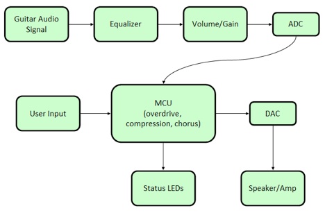
Block diagram of the pedalboard system.

Boss BCB-60 Pedal Board with Digital Delay, Phase Shifter, Compression, Distortion, and Equalizer effects. Image taken from http://www.boss.us
Concept
Our design is modeled off the many commercially available guitar pedals and effects units. Most standard guitar pedals will have a large switch, or “pedal”, that toggles an effect on or off. Each pedal will also often have additional knobs, which will change some parameters of the effect (such as how strong the effect is). These knobs usually need not be easily accessible while playing, as in most cases effect parameters are not changed in the middle of a song.
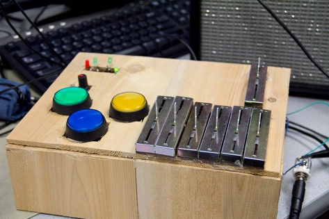
Our concept followed this idea closely; the user would step on a large button while playing to activate an effect. A knob is also used to adjust the parameters of one of the effects. Also, LEDs are used to tell the user which effects are currently on. Standard 1/4” instrument cables can be plugged into the input and output jacks of the effects unit.
A total of five effects have been implemented: volume control, equalizer, overdrive/distortion, compression, and chorus. The pedalboard will process 16-bit audio at a variable rate that depends on the number of effects that are active; however it will be at least 25kHz.
General Hardware
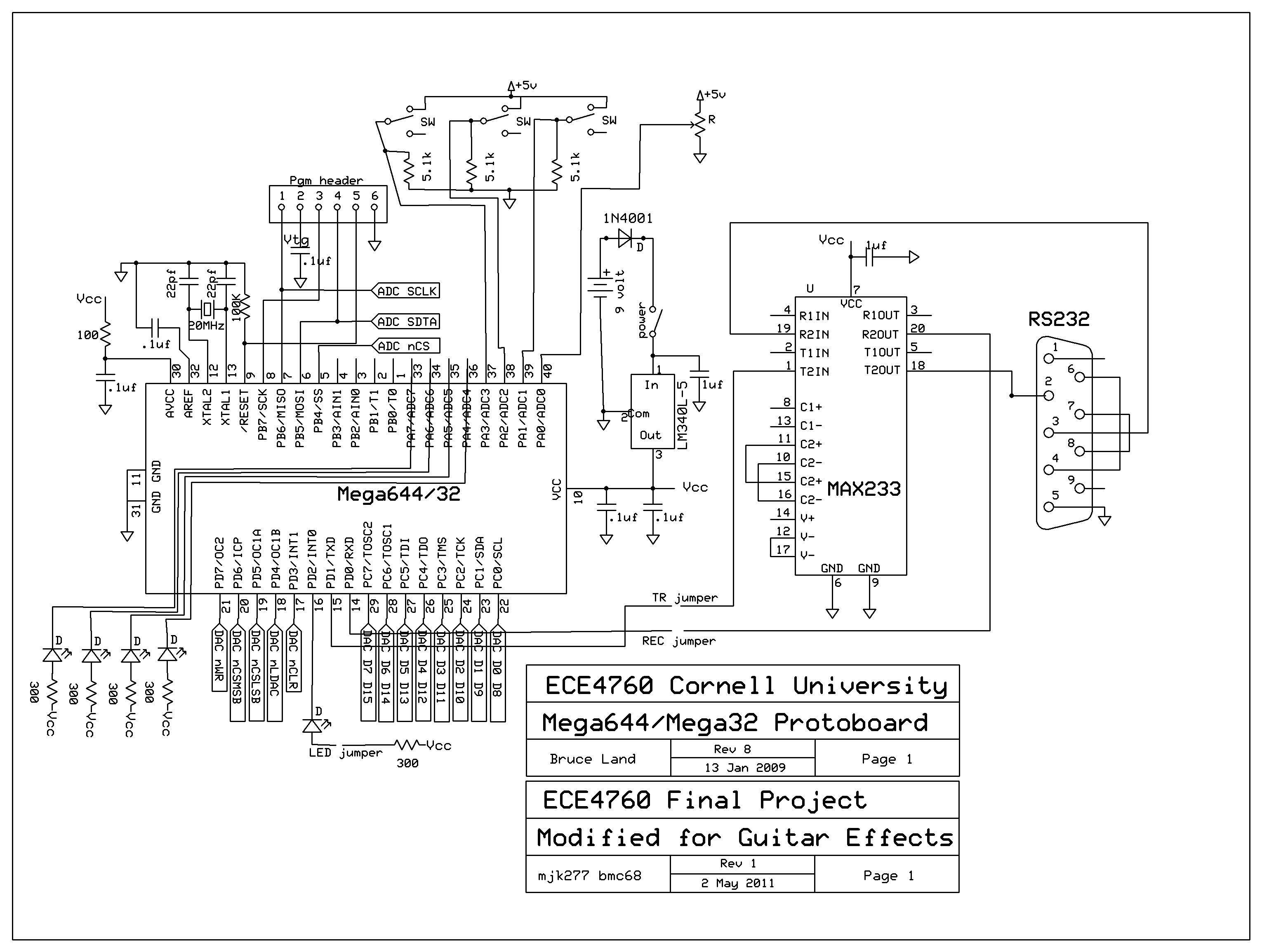
We used the PCB designed by Bruce Land specifically for this class to house the Mega644 chip. The chip includes a serial output for the UART interface, as well as an RS232 connection for programming. We used a 20 MHz crystal to clock the MCU; this choice was made to speed up the sampling rate of the audio.
Additional hardware components include active low pushbutton circuits designed to output 0 V when the pushbutton is pressed, and LEDs connected to port pins (in series with 2K resistors) to indicate which effects are on.
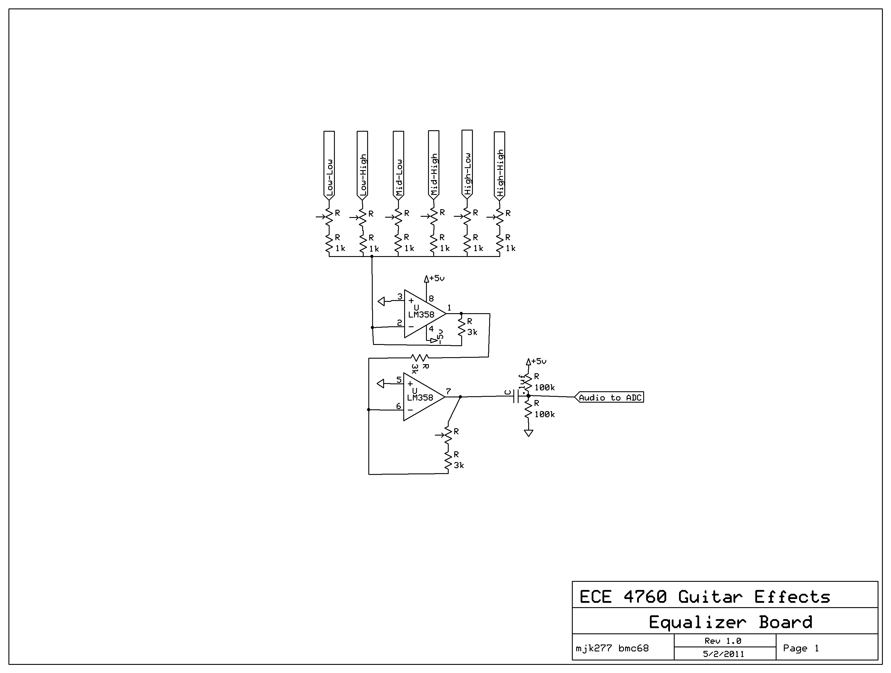
Equalizer and Volume Control
The equalizer and volume control were all hardware based, primarily using active bandpass filters and op-amp circuits to achieve amplification and filtering. The basic design of the op-amp filter is shown below.
Overdrive/Distortion
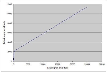
The mode of this effect (off/overdrive/distortion) is determined by the variable OD, which cycles through the three states at the press of the corresponding pushbutton. In the off state, no effect is applied. In overdrive state, soft clipping is applied through the application of a cube law. With the input x scaled appropriately so that the value is within the signed int range, the equation used was ((–x3/228)+x). In order to save processing time by avoiding a float multiply, the cube calculation was done in three steps; by first calculating the square, shifting the 32 bit product right by 16 bits, and multiplying again. A graph of the input-output characteristic is shown below.
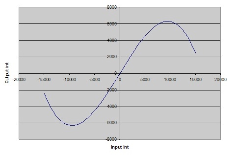
Graph of the overdrive input/output characteristic.
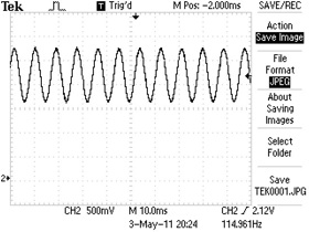
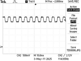
Output of the pedalboard for a sine wave input without overdrive applied (left) and with overdrive applied (right).
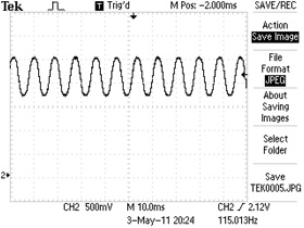
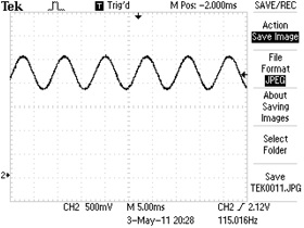
Output of the pedalboard for a sine wave input with distortion applied.
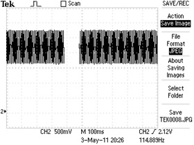
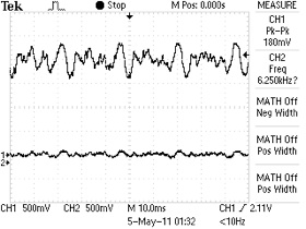
Output of the pedalboard for a sine wave input without chorus applied (left) and with chorus applied (right).

Graph of the input-output characteristic of the compressor. Note that compression is based on signal amplitude.
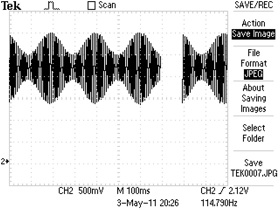
Output of the pedalboard for a sine wave input without compression applied (left) and with compression applied (right). The original signal was fairly high in amplitude, so it was attenuated.
Speed of Execution
Overall, the code that we wrote executes quite quickly, showing basically no delay in reacting to user inputs such as enabling an effect, changing the gain, or changing the equalizer pattern. Time delay only becomes a large factor when all three effects are enabled at the same time. This is because the sum of the code that is run when all three effects are enabled prevents the ADC from sampling at greater than 44 kilo-samples per second (with all three effects on, the sampling rate was about 20 kHz). At very high audio frequencies anti-aliasing could occur, causing undesirable effects on output.
Accuracy
The quality of the signal after it has passed through the board is very good with a little noise due to various sources of interference such as 60Hz or wires close to one another in the circuitry. If one is to only use one effect, the accuracy of the signal produced does decrease. This is due to the fact that while the speed of the alternating signal increases the sampling rate of the ADC stays current. This in turn leaves out more and more details as the frequency increases. In theory, one could increase the signal to a point at which the ADC would only be able to capture one point on the rising edge and one point on the falling edge, making for a horrible approximation. Luckily this point operates outside of the scope of frequencies we need to operate for this project. While this extreme example may not be of a concern to us, the loss of good signal approximation can and does occur as frequency increases.
Enforcing Safety in the Design
In order to prevent an electrocution hazard, we have decided to cover the electronic components in a wooden box with only the switches, LEDs, and potentiometers easily accessible to the user. We have left a hole in the back of the box so that the components may be accessible if needed. However, the cover is in place to prevent inadvertent touching of the components which may cause ESD or perhaps harm the user through the highly unlikely event of electrocution.
Usability
The user interface was meant to be intuitive. The switches for the three effects are quite large so that they could be pressed with a foot. Furthermore, the chorus effect has an additional potentiometer which modifies the effect. This potentiometer is intuitively placed above the button which controls the effect. The equalizer sliders are placed in such a fashion that each successive slider from left to right modifies higher and higher frequencies. The gain slider is placed separately from the equalizer sliders so that they are not confused with each other. Finally, there are LEDs indicating power, the compression effect, the overdrive effect, and the chorus effect so that the user may know when the system is on and under which mode it is operating.
The linear term in the cubic equation dominates at low levels of output, but the cubic term attenuates the signal at high values. The result is a waveform with flatter but still curved peaks. In the case that the absolute value of the input signal is over 10000, the attenuation of the signal becomes too strong. However, with the amplification levels in the circuit, the signal value will only get that high if one makes a conscious attempt to do so – in this case, the possibility of broken strings will be a greater cause of concern than an over-attenuated signal.
The distortion algorithm is much simpler; if the value of the input coming from the ADC is within about 3000 of the base value, then the signal will be unaltered. However, if the input value is outside of this range, the value will automatically be reset to be 3000 above (or below) the base value. This will result in perfectly flattened signal peaks.
This effect is the most computationally heavy; taking over 400 cycles on the overdrive setting. This is mainly due to the two long multiplications that take place. The time it takes to process the overdrive is one of the reasons that the standard 44.1 kHz sampling rate could not be perpetually achieved.
Chorus
The chorus effect, which mixes in pitch modulated signals with the original signal, made use of a trigonometric identity to greatly simplify the calculation while still maintaining effect integrity. According to the product-to-sum identity, the product of two sine waves has frequency components at the sum and difference of the two initial sine waves. We used this identity to create pitch modulations; by multiplying the original signals by a low frequency sine wave, it was possible to create two pitch modulated versions of the original signal.
The low frequency sine wave was generated using direct digital synthesis; a 1024 value sine table was created, and this table was stepped through using a timer interrupt. The frequency of this sine wave was about 8 Hz. This frequency was high enough so that there would be no audible enveloping of the processed signal, and low enough so that the pitch modulated components still had a similar pitch. This signal was then scaled with a shift so that it would be about half the amplitude of the original signal, then added to the original signal (shifted right one bit). The ratio of mixed signal to original signal can be altered by turning the potentiometer knob; the ADC will read in it’s value, and change the scaling of the original and mixed signals accordingly. At the highest setting, the waveform will be noticeably enveloped (see picture below).
The chorus effect is not as computationally heavy as the overdrive, but it will still take over 100 cycles as there is one long multiply (multiplication by the low frequency sine wave).
Compression
The compression effect used a mathematical approximation to compress the dynamic range of the signal. Compression works similarly to the overdrive effect where the higher values are attenuated, but is based on the amplitude of the signal and not the value of the signal. Therefore, it is important to look only at the peaks of the waveform when compression is applied. In our algorithm, a value must satisfy three conditions to be classified as a peak. It must first be greater than the value that comes before and after it, thereby being a local maximum. The second condition is that the value must be greater than 500 above the base (no signal) value. This is to prevent noise from triggering peaks. Lastly, the value must be greater than 3000 (a significantly high value) or within 300 of the previous peak. These conditions account for the two situations in which peaks will occur: when a note is first played, and the “ringing” that occurs after a note is played.
Based on the measured peak value, a scale factor is then computed, and the signal is multiplied by this factor. The equation for the scale factor is: ((32768/peak)+3)/8. A graph showing the input-output characteristics is shown above. An important note is that this computation takes place in 3 steps in order to avoid an integer divide, which introduces some inaccuracy due to rounding. Also, for low values of the signal, a constant scale factor of 8 is applied in order to prevent the scale factor from growing absurdly large for very weak signals.
Analog to Digital Converter Interface
In the control and data gathering from the AD7680, the Serial Peripheral Interface was used. Therefore, it was essential to initialize the SPI in the init() function. Firstly, the direction of the pins in PORTB had to be set. nCS, and SCLK are both outputs from the MCU while MISO is an input from the ADC to the MCU. Therefore, DDB4 and DDB7 were set to 1. Now that the port directions were set, the SPI could be enabled and configured through the SPCR and SPSR registers. Under SPCR, we enable SPI, set MSB first, set the ATmega644 as the master, setup on the falling edge and sample on the rising edge. Furthermore, the SPI2X bit is set to 1 in SPSR to enable SPI to run at 10MHz since it divides the oscillator speed by 2.
Now that SPI has been initialized, readData() can be called to poll and retrieve a 16 bit value from the ADC. In readData(), PORTB.4 is set low to select the ADC and 3 bytes of “junk” data are sent to the ADC via the SPI_MasterTransmit() function which sends out data via the SPDR register. What is being sent is not significant. Rather, the SCLK signal generated from the 3 bytes being sent is significant since that signal enables the ADC to send back data in the SPDR register via nCS. In readData() as each byte is sent, the byte received from the DAC is stored in Ain1, Ain2, and Ain3 respectively. The nCS is set high again on PORTD.4. To leave the DAC open to complete another operation. Since 24 clock cycles are passed to the ADC per its requirements, the ADC buffers the data with 4 zeros before the data and after the data. Therefore, it is essential to shift the data received to get the desired 16-bit output. In our case, Ain1 is shifted to the left by 11 bits, Ain2 is shifted to the left by 3 bits, and Ain3 is shifted to the right by 5 bits. The resulting 160bits are stored in Atot to be used in signal processing and the output signal.
Digital to Analog Converter Interface
As with the ADC, the DAC must have pins and ports initialized so that it may function correctly. In the case of the LTC1657, the initialization is perhaps simpler since there is no SPI to configure, only the directions of the needed ports. In our setup, all of PORTC is set to output (0xFF) as are pins D.7 for nWR, D.6 for nCSMSB, D.5 for nCSLSB, D.4 for nLDAC, and D.3 for nCLR. As part of initialization the nCLR pins is briefly set low in order to clear any settings that might have been set during startup.
With the DAC initialized, one may call writeDAC(uint16_t data) to write a value to the DAC and output the value on the DAC’s output pin. In order to accomplish this task, the data is first split into two characters: upper, lower. Upper consists of data shifted to the right by 8 bits while lower is just the first 8 bits of data. The splitting of data is necessary to conserve port space on the MCU. While the DAC does support writing 16 bits at a time, it is more practical and cost-effective for us to write the data to the DAC as two separate bytes. To write to the DAC, the nWR is first set low so that the DAC know that data will be sent. The nCSMSB is set low so that the DAC knows the MSB will be sent and then upper issent over PORTC. nCSMSB is then set high and nCSLSB is set low with lower sent over PORTC. After the two bytes are sent, nCSLSB is set high as is nWR. nLDAC is then toggled low and then high to let the DAC know that it can output the voltage on its output pin.
The pedalboard performed relatively well; all five of the implemented effects were noticeable in the output signal (which was hooked up to an amplifier and a speaker). The ADC and DAC functioned well, communicating correctly with the microcontroller. The user controls were responsive aside from the large pushbuttons, which required a long press to toggle. The sound quality of the processed signal was mediocre; there was a lot of crackling and high frequency noise in the output signal which was due to either a noisy power source, or the capacitors in the equalizer band-pass circuits.
Each of the effects performed the desired effect on the input sound signal. The volume slider was able to reduce the signal gain to almost nothing, while also being able to increase that gain to the point where the signal value would clip at the source voltage of 5 volts. Most of the equalizer controls were functional as well, except a few that were not as responsive. We believe that this is most likely due to faulty capacitors or bad solder connections within the circuit. The overdrive effect worked very well as long as the volume was turned up sufficiently high; the overdrive setting would add a subtle warmth to the sound while the distortion setting added harsh, gritty distortions to the sound. The chorus effect also adds a subtle change to the sound unless it is turned up to the highest setting where enveloping by the low frequency sine wave is audible. Lastly, the compressor worked more to reduce loud sounds while leaving soft sounds the same volume. While this was not the intended behavior of the effect, it is still beneficial as it decreases the dynamic range by reducing the gap between loud and soft playing.
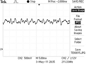
Output of the pedalboard for guitar input without no effects applied(left) and with all three effects applied (right).
Video demonstration of the compact guitar pedalboard.
ADC and DAC Hardware Interface with Microcontroller
The analog-to-digital converter we chose to use was Analog Devices AD7680. The main reasons for choosing this particular ADC were its resolution of 16-bits and its ability to communicate via SPI which makes it easier to use. Using an ADC with a resolution of 16 bits was quite important to us as this resolution would more closely match the actual sound than the 10-bit ADC on the ATmega644. This was quite apparent in our initial testing as the sounds recorded and played back using just the ATmega644 were somewhat distorted from the original signal. The wiring was quite simple as the whole ADC setup only needed 6 wires and a decoupling capacitor from power to ground. Wires were used for Vdd, Ground, Analog In (From the Equalizer Board), negative Chip Select, Clock (SCLK), and Master In Slave Out (MISO). nCS was attached to PORTB.4, SCLK was attached to PORTB.7, and MISO was attached to PORTB.6 on the microcontroller. The use of the SPI protocol made use of the ADC trivial as a simple toggling of the nCS to the low position would initiate a data acquisition, clocked back over MISO at the tick of the clock on SCLK.
The Digital to Analog Converter we chose to use was Linear Technologies LTC1657. This DAC had a 16 bit output which was necessary in order to prevent the signal from losing quality that had been preserved with the 16-bit DAC. The integrated circuit made use of a parallel interface which consumed all of one port on the microcontroller and then a few more pins for various control bits. In our setup, the 8 bits of data would be transmitted from the microcontroller to the DAC from PORTC. Furthermore, a pin to control writing (nWR) was attached to PORTD.7. nWR is set low when the user wishes to write data to one or both of the data registers. A pin to toggle writing to the MSB of data (nCSMSB) was attached to PORTD.6. This pin would be set low to write to the upper 8-bits of data. The same sort of pin was used for the lower 8-bits, called nCSLSB, and attached to PORTD.5. A pin (nLDAC) was attached to PORTD.4 which set the loaded data to output once toggled low. A pin to clear, nCLR is attached to PORTD.3. This pin would allow the user to write to the DAC in two steps, once for the high byte and once for the low byte, and then toggle the pin to output the new value on the DAC’s output. In wiring the DAC a few other connections had to be made as well. A 0.1 µF decoupling capacitor had to be used to decrease the amount of noise in the signal. This configuration enabled us to output values from 0 to 5V with a step size of 76 microvolts, which is precise enough for our needs.
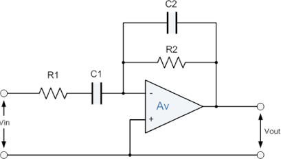
Schematic of op-amp active bandpass filter. R1 and C1 comprise the high pass filter, and R2 and C2 comprise the low pass filter. Image taken from http://www.electronics-tutorials.ws.
The equalizer was comprised of six different sets of active bandpass filters in the inverting configuration. They were tuned so that the pass band frequencies were approximately 100 Hz. 200 Hz, 400 Hz, 800 Hz, 1600 Hz, and 3200 Hz. The resistors R1 and R2 were set to be equal at 5.1 kOhms, so that the gain would be equal to 1. A schematic of the six filters is available in the appendix.
The six outputs from the filters would then be combined in a summing amplifier configuration, using a 100 kOhm logarithmic slide potentiometer to control the gain. The summing amplifier will weight the input voltages according to the values of the input resistors. A basic summing amplifier configuration is shown below. In our design, we placed the potentiometers in parallel with the static input resistors. Increasing the value of the potentiometer would work to decrease the signal gain for a particular band.
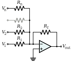
Basic schematic of summing amplifier. Taken from http://www.wikipedia.org.
The volume control unit was built similarly to the op-amp filter, but without capacitors as filtering was not necessary. A 100 kOhm potentiometer was placed in series with the feedback resistor to control gain from +3 (+5dB) to -33 (-15 dB).
All operational amplifiers were powered with dual power supplies at +5 V and -5 V. -5 V was generated by using a negative voltage regulator (ICL7660).
Meeting Expectations
In looking at the design, I can say that the majority of our expectations were met. We were able to include an equalizer on our board along with gain/volume control. We were even able to assemble a case for the equalizer so that the user would not have to see the insides or expose themselves to a potential electrocution hazard when using the device. We were also able to include two out of the three effects we had initially planned to do: compression and distortion. The third effect, delay, was replaced with chorus since we did not have enough pins to use an EEPROM needed for the effect. Other than that, we met the goals we had in mind when we set out to do the project.
If we were to do this project again, there are a couple things we would do differently the next time around. For one, we would have ordered some of the parts earlier so that we could test them out sooner. Some of the parts we ordered arrived only a couple weeks before the project due date. One example of this is the sliders, which we needed to implement the equalizer. While we had successfully implemented the equalizer using trimmer potentiometers we did not use the sliders in the project until about 2 weeks before the due date of the project. While the sliders worked out fine in the end, it would have been nice to have more wiggle room to work with them since there was some ambiguity in pin assignments on the sliders. Another thing we would definitely do differently the next time is write the report as the project is being completed. We waited to write the report until the project was basically done. While this would work in most cases, the last week of classes is an instance where this does not work. Having to write the report too while testing the pedal board and completing projects for other classes was pretty stressful and we would rather not have to do that again. Overall, we would practice different time management skills if we were to do this project again.
Areas of Further Research
There are a few areas in which more research could be done to make the project better in the future. For one, a software equalizer could be implemented. While this would create added complexity in the code, it would definitely decrease the amount of wiring involved. Honestly, it would probably look pretty impressive if there was an LCD screen giving feedback about equalizer status too. Another area where more research could be done is adding additional effects. While we only did compression, overdrive, and chorus, there are many more effects that can be done. We just chose to do these effects because of their familiarity. There is nothing stopping an adventurous person from implementing additional effects though. Finally, the hardware could be changed or software reorganized to allow for enough pins to implement the delay effect.
Legal and Ethical Considerations
In the designing and construction of our project, we strove for consistency with the IEEE Code of Ethics. In creating a case for the project, it was our not only our goal to create an aesthetic housing for the project but to protect the user from any inadvertent electrocution hazards. This is consistent with the first tenet of the Code of Conduct which states that one makes “decisions consistent with the safety, health and welfare of the public.” When it came time to write our report, we avoided exaggerating what our project could do and tried to be as factual as possible so that our accomplishments in completing this project would not be inflated. Our project tried to avoid conflicts of interest such as product placement or the like, and when we did source parts as samples we disclosed this on our parts list. In the writing of our report, we strove to be honest with our own technical work through crediting those responsible for the general guitar effect algorithms and taking care not to obfuscate our technical errors in the implementation of our project. Finally, we strove to create a project that could be used by all people. The only group that might have trouble using the project would be those who are deaf. Since our project deals with modifying sound waves, they will not be able to tell whether it is working or not. Those who are blind can still use the project once they memorize the locations of the controls, which should take just a short amount of time.
In terms of intellectual property considerations, we will be using code that has been given to us for past ECE 4760 projects in the implementation of the pedal board. We also used the UART code by Professor Land for testing purposes. We do not believe we have infringed upon any patents in the course of making this project. With all of the products commercially available, we believe that pursuing a patent (or publication) is not very realistic for this project.
Division of Labor
Michael
-Coding functions to communicate with ADC and DAC
-Soldering the Equalizer, Filter, and ADC/DAC boards
-Drawing the Schematics
-Acquiring extra proto-board and MCU from Cornell Baja SAE
-Breaking code up into functions
-Writing part of the report
Brian
-Designing the Equalizer and Filter Boards
-Coding compression, overdrive, and chorus effects
-Ordering parts
-Building case
-Writing part of the report
-Converting report text to web page
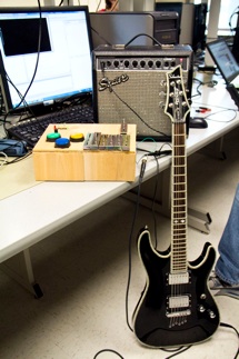
Finished pedalboard with casing.
Acknowlegements
We would like to thank Bruce Land as well as all of the TAs for ECE 4760 for making the course (and this final project) enjoyable (and less painful) will all of their help and advice. We would also like to thank all the other students in the class for bearing with our loud and ugly noises.
Additional Information
Link to commented code: finalproj_compression.c
Schematics: Protoboard.bmp FilterBoard.bmp EqualizerBoard.bmp
Budget: table.html
Appendix
Copyright 2011, Brian Choi, Michael Kilzer
