"A digital stethoscope that can amplify, play, and record heart signals in real-time."
Project Soundbyte
The purpose of this project was to design and implement a digital stethoscope to serve as a platform for potential computer aided diagnosis (CAD) applications for the detection of cardiac murmurs. The system uses a custom-built sensor to capture heart sounds at 8 kHz and converts them to electrical signals to be processed by an ATmega644 microcontroller. The captured signals are outputted via pulse-width modulation to a standard 3.5 mm audio socket for real-time auscultation. In addition, the stethoscope uses a 1MB external Flash memory chip to record and playback audio waveforms. For the user interface, the system includes a 4-line 20-character wide LCD display and a 16-button keypad. Real-time and recorded data can also be visualized using a MATLAB interface that runs on a separate PC and connects to the stethoscope system via the USART interface on the microcontroller. The MATLAB interface also uses the transmitted data to calculate and display the patient’s average heart rate in beats per minute.
This project is meant to provide a framework for developing useful embedded CAD tools for cardiac murmur detection. Heart murmurs may go unnoticed during routine check-ups since detection relies on the training of physicians, the quality of the equipment used, and the severity of the condition. A digital stethoscope can be used to assist physicians in analyzing cardiac signals in real time during auscultation to reduce the risks of not detecting certain conditions.

Figure 1. Digital Stethoscope System
High Level Design top
Overview
The overall architecture of the system is centered on the ATmega644 microcontroller. The acoustic sensor and keypad are inputs to the MCU, while the LCD, headphones, and MATLAB visualization tool are outputs. Communication with the Flash memory is bi-directional. Figure 2 shows an overview of the system high level design.
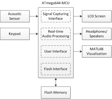
Figure 2. System High Level Design
The MCU runs several software interfaces to support the various features of the digital stethoscope. The signal capturing interface uses the analog-to-digital converter to sample the acoustic sensor at 8 kHz. The real-time audio processing module modifies the measured signal based on user settings and outputs it to the 3.5 mm audio socket via pulse-width modulation. The user interface supports the detection and de-bouncing of keypad button presses as well as controls the LCD display to reflect the current state of the system. In addition, the user interface also outputs real-time or recorded data at 100 Hz to a MATLAB utility running on a separate PC for signal visualization and average heart rate calculations. The Flash interface includes a software library for SPI communication to read from and write data to the external Flash memory chip.
Hardware Design & Implementation top
Stethoscope Acoustic Sensor
The stethoscope acoustic sensor was an integral hardware component of the system. The quality of the sensor directly impacts the quality of the real-time audio output as well as all analyses performed on the measured waveforms. Because of this, a custom sensor was designed and developed to capture heart signals. The sensor includes a standard stethoscope chest piece to amplify acoustic signals and an electret condenser microphone to convert the amplified signals to electrical waveforms. A microphone with a 20 Hz – 20 kHz frequency range was selected in order to capture all of the low frequencies characteristic of internal body sounds. The microphone was placed within a rubber tubing as close as possible to the base of the chest piece. In order to reduce noise and improve convenience, a 3.5 mm shielded cable was soldered to the leads of the microphone and pulled through the rubber tubing to interface with the MCU. Figure 3 shows an image of the constructed stethoscope sensor.
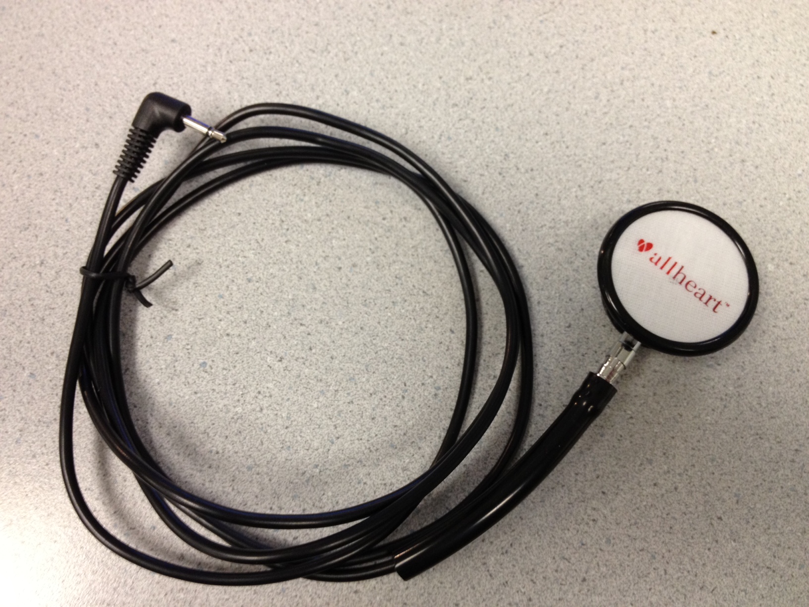
Figure 3. Stethoscope Acoustic Sensor
The sensor construction was tested by using a multimeter to detect shorts and to verify that proper connections were made. The actual sensing capability of the component was tested using the bias/amplifier circuit described in the next section.
Microphone Bias and Amplifier Circuit
The microphone in the acoustic sensor needed to be biased in order for proper operation. In addition, the output of the microphone is on the order of millivolts, which is relatively small in magnitude compared to the precision of the ADC sampling the sensor (the ADC has a precision of approximately 20 mV when taking 8-bit samples). This makes it challenging for the microcontroller to detect changes in sensor output. In order to address both these issues, a bias and amplifier circuit was designed and implemented to interface the raw sensor output with the MCU. The goal of the circuit was to properly bias the microphone and amplify the sensor output to detect voltage swings caused by sounds. The figure below shows a schematic of the completed circuit.
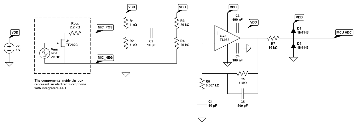
Figure 4. Microphone Bias and Amplifier Circuit
The typical operating range for the microphone was 2 V, with a maximum rating of 10 V. The MCU provided a voltage of 5 V, so a simple voltage divider circuit with identical 1k resistors was used to reduce the voltage to 2.5 V to bias the microphone. The output of the microphone was passed through a capacitor to remove the DC offset. The capacitor used was large enough to make sure that the desired low frequencies were not filtered out. With two 1k resistors in parallel with the output of the microphone, the equivalent output impedance of the sensor is roughly 400 ohms. Using a 10 uF capacitor, a simple high pass filter with a cutoff frequency around 40 Hz was designed, which is below most of the low frequencies of interest.
The AC-coupled signal was connected to the positive input (Vin+) of an operational amplifier to boost the signal amplitude. Because the microcontroller ADC measures voltages between 0 and 5 V, the Vin+ line of the op-amp was biased to 2.5 V in order to capture the largest magnitude of positive and negative swings from the microphone output. This biasing was implemented with another voltage divider circuit using identical 20k resistors. The values of these resistors were chosen to be larger than the resistors in the previous voltage divider in order to avoid affecting the equivalent output impedance of the previous stage.
For signal amplification, a non-inverting op-amp configuration was used. The gain of the circuit is defined by the following equation:

The resistors were selected to achieve an ideal gain of 150 for frequencies between the range of 20 Hz and 2 kHz. The gain was selected based on the 300 kHz gain-bandwidth product constraint of the op-amp. *Note: the resistor R6 was implemented in hardware as a variable resistor (10k trimpot) in order to allow for more convenient prototyping and testing. A capacitor was added in series with resistor R6 in the op-amp feedback loop to create a system with unity gain for DC voltage inputs. The unity gain at DC is important to prevent amplification of the 2.5 V bias at the Vin+ node. Without this additional capacitor, the output of the amplifier would saturate to 5 V when the microphone did not detect any sounds. A 10 uF capacitor was selected for C1 in order to achieve a high pass filter cutoff of approximately 2 Hz, which is close to DC in order to pass all non-DC signals. On the other hand, a 500 pF capacitor was selected for C5 in parallel with a 1M resistor in order to create a low-pass filter with a cutoff frequency of approximately 300 Hz. With all of these basic hardware filter realizations, the effective frequency range of the filtered output signal is between 40 – 300 Hz.
For stability, 0.1 uF decoupling capacitors were added in parallel to the Vcc and Gnd nodes of the op-amp. And to protect the ADC pin on the MCU, protective diodes and a 10k series resistor were added to the circuit.
The amplifier circuitry was thoroughly tested after it was built on the breadboard. A function generator was connected to the input of the circuit and frequencies were manually swept to test and verify the circuit’s frequency response. The following table and plot shows the measured frequency response of the microphone circuit:
Microphone Circuit Frequency Response Results
| Input Frequency (Hz) | Input Peak-to-Peak (mV) | Output Peak-to-Peak (mV) | Gain (abs) | Gain (dB) |
|---|---|---|---|---|
| 20 | 2.08 | 272 | 130.77 | 42.33 |
| 50 | 2.08 | 272 | 130.77 | 42.33 |
| 100 | 2.08 | 264 | 126.92 | 42.07 |
| 150 | 2.08 | 248 | 119.23 | 41.53 |
| 200 | 2.08 | 232 | 111.54 | 40.95 |
| 250 | 2.08 | 216 | 103.85 | 40.32 |
| 300 | 2.08 | 200 | 96.15 | 39.66 |
| 500 | 2.08 | 152 | 73.08 | 37.28 |
| 1000 | 2.08 | 88 | 42.31 | 32.53 |
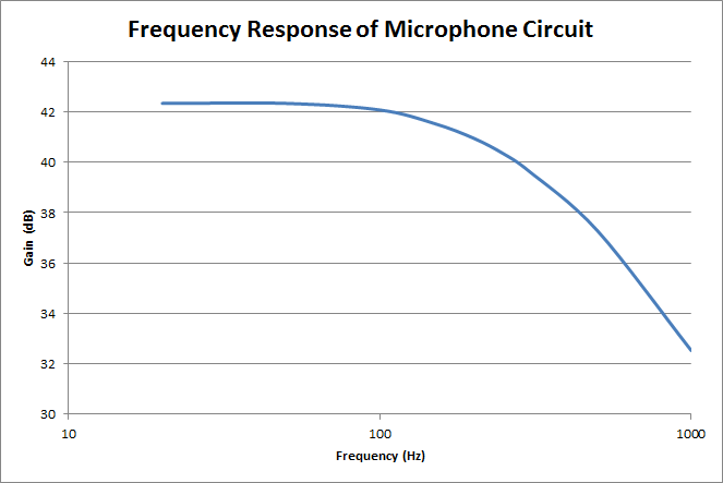
Figure 5. Microphone Circuit Frequency Response
The measured data shows that there is approximately a 3dB drop in gain at the 300 Hz cutoff frequency. This shows that the implementation of the low pass filter properly attenuates high frequency signals. After verifying that the frequency response of the circuit was as expected, the acoustic sensor was tested by connecting it to the input of the bias/amplifier circuit.
Digital-to-Analog Converter
In order to output the real-time or recorded audio waveform to a headphone/speaker, a simple digital-to-analog converter was implemented in the form of an RC low-pass filter. This circuit averages a pulse-width modulated input signal in addition to attenuating high frequency content. Figure 6 shows a schematic of the DAC circuit.
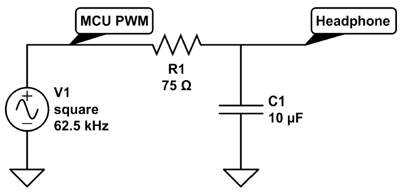
Figure 6. Digital-to-Analog Circuit for Audio Output
The RC time constant of the filter was designed to attenuate frequencies higher than approximately 210 Hz. This cutoff frequency is below the frequency range of the input signal to the MCU. The circuit was designed this way in order to reduce higher frequency noise introduced to the signal at the PWM output. A relatively small resistor value was chosen for the circuit in order to interface with low input impedance headphones.
The circuit was tested and validated using the stethoscope sensor and amplifier circuit after the software to capture the stethoscope output and generate the PWM signal was developed. The figure below shows the PWM signal and corresponding analog signal captured on an oscilloscope.
Flash Memory
A 1MB Flash memory chip was acquired to provide the capacity to store up to 10 cardiac waveforms for future playback and analysis. Since the chip requires a supply voltage between 2.7 V and 3.6 V, a power regulator was used to convert the 5 V supply powering the rest of the circuit to a stable 3.3 V supply for the memory. The microcontroller communicated with the Flash chip through a serial peripheral interface (SPI), with the MCU as the master and the Flash chip as the slave device. The SPI bus specifies four logic lines: serial clock (SCLK), master output (MOSI), master input (MISO), and slave select (SS). The SCLK, MOSI, and SS lines are outputted by the MCU and therefore require level shifting from 5 V to approximately 3.3 V. The MISO line is outputted by the Flash memory and does not require any voltage translation to interface with the MCU. This is because the 3.3 V output of the memory is within the lower bound to detect an input high voltage on the I/O pin. Figure 7 shows a schematic of the flash memory circuit.
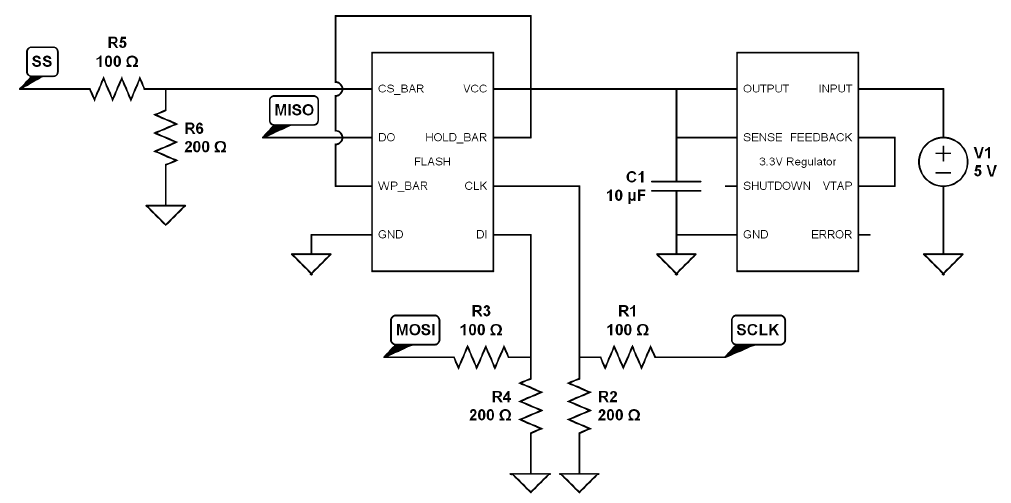
Figure 7. Flash Memory and Voltage Regulator Circuits
Voltage translation was implemented using simple resistive dividers. The values of the resistors were selected to be small in order to reduce the RC time constant of the translation. This was necessary in order to cleanly level shift the high frequency clock signal without distortion.
To test the read functionality of the Flash memory, a short segment of code was written to send a command from the microcontroller to read the memory chip manufacturer’s ID. To test the erase and write functionalities, a sector erase followed by a page write command were sent to the chip to store data. A data read command was then issued to verify that the contents of the memory were correct.
Keypad and LCD
A 16-button keypad and 4-line 20-character wide LCD display were used for the primary user interface of the system. The two components were directly connected to I/O pins on the microcontroller and did not require any extra hardware circuitry for operation.
Software Design & Implementation top
The overall software for the project consisted of embedded code running on the Atmega644 microcontroller and a MATLAB visualization tool on a PC.
ATmega644 Microcontroller
The microcontroller served as the central system component. The software running on the microcontroller was responsible for sampling the stethoscope sensor output, generating a PWM signal for audio playback, adjusting the volume of the audio output, storing the acquired data in Flash memory for later playback, and transmitting data to the MATLAB visualization tool. Figure 8 shows an overview of the software system architecture.
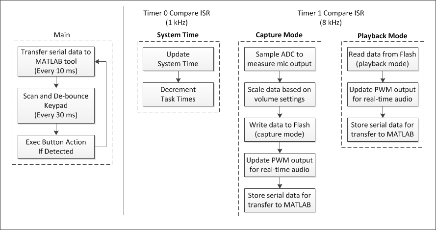
Figure 8. System Software High Level Overview
Signal Acquisition
The ADC module was used to convert the analog electrical signal from the output of the sensor circuit into a digital signal that the microcontroller can process. The voltage reference for the ADC module was set to 5 V. The system clock running at 16 MHz was divided by 32 to drive the ADC at a frequency of 500 kHz. The Timer 1 Capture ISR was used to sample the ADC at 8 kHz with 8-bit precision. Although the frequency content of most internal body sounds are relatively low (< 300 Hz), a higher sampling rate was used to improve the audio quality of the acquired signal. *Note: the minimum sampling rate needed to reconstruct a 300 Hz signal without aliasing is 600 Hz based on the Nyquist sampling theorem. Within the ISR, the sampled data is then scaled based on the current volume settings and written to a flash buffer in the MCU if the system is in capture mode.
PWM Waveform Generation and Serial Data Transfer
Cardiac waveforms were played in real time and from previous recordings by generating a PWM signal using the sampled data from the ADC. A 62.5 kHz PWM output was produced using Timer 2. The magnitude of the output is updated within the Timer 1 Capture ISR at the same 8 kHz sampling rate based on the sampled or recorded data. In addition to outputting the audio data to headphones/speakers, the data is also transmitted to a MATLAB visualization tool via the USART module at 100 Hz. Since the serial transfer task is non-critical, the data is only written to a serial transfer buffer within the Timer 1 ISR. The actual transmission of the data using the USART is performed within the main loop based on system and task times updated using the Timer 0 Compare ISR.
Flash Operations
The software interface with the Flash memory chip utilized the SPI hardware module in the microcontroller. To send a command via SPI, the slave select line was first enabled. The desired transmit data was then written to the SPI data register, which outputs the clock signal on the SCLK line and shifts the data bits (MSB first) out onto the MOSI line. After sending all data bytes, the slave select line was disabled to execute the command in the memory. *Note: SPI communication is full-duplex. As each bit is shifted out onto the MOSI line, a new bit is shifted in from the MISO line. Because of this, dummy data can be sent from the master in order to receive data from the slave. The table below lists the major Flash commands used to read, erase, and write data to the chip.
| Command | Instruction Code | Description |
|---|---|---|
| Page Program | 0x02 | Program up to 256 bytes of data at erased locations |
| Read Data | 0x03 | Read 1 or more bytes of data sequentially |
| Read Status Register-1 | 0x05 | Reads the 8-bit status register-1 |
| Write Enable | 0x06 | Must be executed before writing or erasing data |
| Sector Erase | 0x20 | Erases a 4KB sector of memory |
| Read Manufacturer ID | 0x90 | Reads the manufacturer ID of the chip |
| Chip Erase | 0xC7 | Erases the entire Flash memory |
| Block Erase (64 KB) | 0xD8 | Erases a 64 KB block of memory |
Flash Commands
Writing Acquired Data
In order to minimize SPI communication overhead, captured signal data is first written to a Flash write buffer in the Timer 1 ISR. An SPI page program command is only sent after 256 bytes of data have been collected in the buffer. Each audio recording is allocated 64KB of memory, which corresponds to approximately 8 seconds of recording data when sampling at 8 kHz. This size was chosen in order to fit all of the data within a single block.
Reading Recorded Data
In order to playback recorded data, it is necessary to read data from the Flash memory. This is done one page at a time using two Flash read buffers in the MCU. The playback data is first initialized by reading two pages of data and storing it in the read buffers. The data in the buffers are then output at 8 kHz using the PWM. After a full page of data has been output to the headphones, the second buffer is used to continue the operation. When the buffer switches, a Flash read command is issued to re-populate the original buffer. This process continues until all 64KB of data has been read from memory and outputted to the headphones.
Managing Recording Data
The digital stethoscope system supports saving up to 10 different waveform recordings. Each recording is assigned an ID between 0 and 9. Each recording is also allocated a separate 64KB block of Flash memory. A special 16-bit location in Flash memory is interpreted as a recording status register, which indicates which recordings are valid and stored in memory. This is done through a simple one-hot encoding scheme where the recording ID corresponds to the bit position in the register. For instance, if bit 3 in the recording register is set to 1, then that means that recording 3 is stored in the Flash memory at its specific block address. If the bit value is set to 0, then the recording is not stored in memory.
When initializing the system on power-up, the MCU reads a special “signature” memory address to identify whether the project signature has been written to the chip. The signature indicates that the Flash memory has been properly formatted and the data in the recording status register is valid. If the signature is not found, the chip is erased and the recording status register is programmed to have a value of 0x0000, which indicates that no recording data is stored on the chip.
Keypad and LCD Operation
The primary user interface for controlling the microcontroller consisted of the keypad and the LCD display. The keypad was used to toggle between several modes of operation to record cardiac waveforms, play them back, and adjust the volume settings. The LCD was used to display instructions and visually see that the system was setting parameters and switching between operating modes as expected. The microcontroller software was thus responsible for the operation of these two hardware components, periodically checking the state of the keypad, de-bouncing button presses, and updating the messages displayed on the LCD.
When a button on the keypad is pressed, two of the eight pins get shorted. A piece of code that collected the values of each of the pins in a single number and mapped the result to a number between 1 and 16 was provided. This value corresponded to index of the button in the 4x4 array of buttons. For example, button A was mapped to a numerical value of 4. This value (butnum) was used in the de-bounce state machine for the system (see Figure 3). If the value was anything other than zero, the system would jump from the default RELEASED_STATE to the MAYBE_PUSH_STATE. If the same button is still pressed (and the value of butnum is not zero), the system jumps to the PUSHED_STATE. If the same button is released, the system goes to the MAYBE_REL_STATE before jumping to the RELEASED_STATE and setting a tag to indicate that a button was pressed and released. The button verication and de-bounce code is executed every 30 ms. The value of butnum was mapped to the actual numerical values 0-9 if one of those buttons was pressed. The buttons corresponding to the asterisk (*), pound symbol (#), and the letters were mapped to 11-15 in that respective order. These mappings were stored in the global variable keynumber and were used to evaluate button actions. Figure 9 below demonstrates the state machine used to de-bounce a button press.
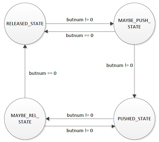
Figure 9. Keypad De-bounce State Machine
The system used several states to differentiate between when a user could specify a setting and when an input wouldn't be registered. In the default state, the system sampled the stethoscope sensor output, outputted the PWM audio signal, and transmitted the data to the PC in real time. Numbers were used to enter various modes of operation. The asterisk and pound keys served the purpose of clearing or entering previously pressed characters.
When a user selected “1” and pressed the pound symbol, the system would enter a recording mode. The user would enter “A” to start a recording and “B” to end it. After a recording is stopped, the user was given the option to play the recording, delete it, or store the sample to Flash memory for later playback. A confirmation message is then displayed based the user input and the system will return to the default state when “D” is entered. The user could play a previously recorded sample by entering “2” to enter playback mode when the system was in the default state. The user could then press the number corresponding to one of the saved waveforms to play the previously recorded sample. The volume could be adjusted by entering “3” in the default state to enter a volume selection mode and entering a number in the range between “0” and “4”. The lowest setting disables the audio output entirely while the highest one double the amplitude of the voltage swings from their default values to produce a sound that is twice as loud as the default one. The current volume setting and the number of waveforms stored could be displayed on the LCD screen by selecting “4” in the default mode. The table below conveys the button functions in each mode.
| Mode | Button | Function |
|---|---|---|
| Default | 1 | Enter Pre-Recording Mode |
| 2 | Enter Pre-Playback Mode | |
| 3 | Enter Volume Select Mode | |
| 4 | Enter Settings | |
| 5 | Enter Flash Utility Mode | |
| Pre-Recording | A | Start Recording |
| D | Return to Default Mode | |
| Post-Recording | A | Delete Saved Waveform |
| B | Play Saved Waveform | |
| Delete | Any | Return to Default Mode |
| Pre-Playback | 0-9 | Play Saved Waveform |
| Post-Playback | A | Delete Saved Waveform |
| B | Play Saved Waveform | |
| D | Return to Default Mode | |
| Volume Select | 0-9 | Set Volume Level |
| Settings | D | Return to Default Mode |
| Flash Utility | A | Erase Flash Memory |
| D | Return to Default Mode | |
Keypad Button Functions
MATLAB User Interface
A MATLAB program was developed to read data from the microcontroller through a serial connection with a baud rate of 9600 bits per second. The connection port was periodically queried and read. The received data was then processed and displayed on a MATLAB plot in real time. The program was also designed to calculate the beats-per-minute (BPM) of a cardiac waveform in real time as well. An average of a cardiac waveform was taken to filter out ambient noise and detect when voltage spikes from heartbeats in a clean fashion. The average calculation was non-linear, intended to increase drastically at the start of a heartbeat and gradually decay until the next one. The first and second derivatives of the average were taken to determine where those steep spikes occur and thus, record the start time for each heartbeat. By calculating the difference between consecutive start times, it was possible to measure the time for a single heartbeat and to calculate BPM.
Results top
Overall, the digital stethoscope system performed well in terms of audio quality, heart rate detection accuracy, and meeting real-time deadlines. The system successfully captured the heartbeat of various volunteers. The sound of the heartbeat was easily heard using standard headphones, indicating that the PWM audio output of the captured waveform was not significantly distorted by ambient noise. However, the audio became much noisier when a waveform was being recorded to the Flash memory and being subsequently played back.
The MATLAB user interface also met expectations, displaying cardiac waveforms in real time and when a stored waveform was played back as illustrated in the figure below. Several people were tested using the stethoscope to determine the accuracy of the BPM measurement algorithm. After obtaining a measurement using the digital stethoscope, the volunteers also determined their heart rate by holding two fingers to their necks and recording the number of seconds required for 10 heart beats. The results are included in the table below. The largest error between the two measurement techniques for the samples taken was around 6%, suggesting that the BPM measurements displayed on the plot were fairly accurate. It should be noted that there is a degree of uncertainty in measuring heart rate using the method with two fingers.
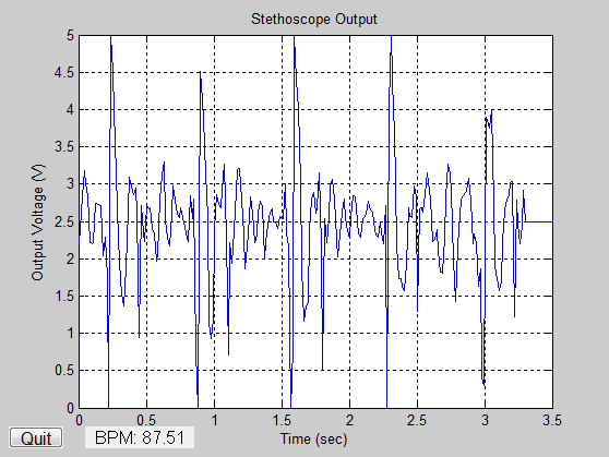
Figure 10. Cardiac Waveform Captured in MATLAB
| Volunteer | Hand Calculation (BPM) | MATLAB Algorithm (BPM) | Percentage Difference |
|---|---|---|---|
| Michael Wu | 82.7 | 83.3 | 0.76 |
| Garen Der-Khachadourian | 82.2 | 86.8 | 5.60 |
| Stephanie Stoughton | 71.4 | 72.6 | 1.68 |
| Stephen Wu | 64.5 | 67.8 | 5.12 |
Heart Rate Measurements
In terms of real-time performance, the software was able to meet the key timing requirements. The most important real-time constraint was the Timer 1 Compare ISR execution speed. The Timer 1 ISR was used to capture and playback audio samples at 8 kHz. In addition, the ISR was also responsible for writing and reading data from the Flash buffers. If the ISR takes too many CPU cycles and interrupts are missed, then the quality of the recording and playback of the audio signal would be reduced. Using simple software profiling, the CPU utilization of the Timer 1 ISR was measured under various conditions. During idle mode when the system samples the acoustic sensor and outputs it to the headphones, the CPU utilization of Timer 1 is approximately 24.75%. During capture mode when the system also stores the sampled data to the Flash write buffer, the utilization is 28.5%. And finally, when the system is in playback mode and reads data from the Flash read buffers to output the recorded sample, the utilization is 5.85%. These values indicate that real-time deadlines are being met, since the only other interrupt service routine is small and only responsible for updating the system and task times.
Since the goal of the project was to develop a system that users would interact with, safety was an important consideration. After the hardware components were prototyped and tested on a breadboard, the circuitry was implemented on a solder board to reduce wire lengths and establish permanent connections. Each hardware feature was then installed into the box enclosure. As a result, the electrical components are protected and the user is able to safely use the system.
Usability was another key consideration during the design process. One of the objectives of the project was to create a fully functional device that a user could easily operate. The keypad and LCD interface provided a user-friendly means to input commands and control the operation of the system. The MATLAB user interface intuitively displayed cardiac waveforms to assist auscultation. A 3.5 mm audio cable was used for the microphone to easily plug the stethoscope sensor into a standard jack, minimizing the wiring of the circuit and providing a clean way for the user to plug the device into the system. The stethoscope chest piece was integrated into the sensor for both functional and aesthetic purposes. The hardware components were embedded to the box to hold the final product in a simple container and provide a friendly interface for the user to plug in the peripheral components. Furthermore, a 9 V battery was included in the system to allow the user to run the system without the need for an external 9 V DC supply. For these reasons, the system’s portability is significant feature that enhances its usability.
Conclusions top
Final Thoughts
The completed digital stethoscope system was able to able to meet the various goals of the project. The system is able to perform the following key features:
1. Capture a cardiac signal using a custom-built acoustic sensor and an analog-to-digital converter
2. Output a real-time audio signal based on the sampled input using a digital-to-analog converter
3. Record and playback captured signals using external Flash memory
4. Transmit real-time and recorded serial data via the USART for visualization and analysis
Although the system meets all of the basic requirements, there is still room for future improvement and optimization. One critical challenge is to identify and remove the noise that pollutes the audio output signal during reading and writing of the Flash memory. This would greatly improve the quality of the recordings that are saved to Flash. For additional features, implementing the MATLAB heart rate detection algorithm in the microcontroller software would be valuable to move the system towards a completely embedded solution. Another useful feature of the stethoscope would be an implementation of software FIR filters to allow users to filter out specific frequency ranges.
In addition to these improvements, a significant extension to this project would be to research and implement an algorithm to detect and classify cardiac murmurs based on the captured waveform data. With a quick online search, it is clear that digital stethoscope systems are commercially available to physicians and other healthcare specialists. However, most of these products do not offer any built-in CAD features to help improve diagnostic abilities. As the computational performance of microcontrollers increase, it is becoming possible for effective CAD applications to be developed for embedded systems. A digital stethoscope with embedded CAD features could help identify cardiac murmurs and other heart conditions, eliminating the need for separate imaging procedures (e.g. echocardiography) for diagnosis.
Intellectual Property Considerations
Several resources were used as references in this project. Bruce Land's keypad de-bounce and LCD display software proved useful in implementing the user interface for the application. Online resources were referenced to implement the MATLAB user interface as well. Each reference is appropriately documented and acknowledged in the References section. There is no intention to pursue the acquisition of a patent for this project. Several patents already exist for digital or electronic stethoscopes. This project was intended as a proof-of-concept.
Legal and Ethical Considerations
The hardware and software design decisions made throughout the project followed the IEEE Code of Ethics. Precautions were taken to ensure that no one was subjected to a situation that involved physical risk and all hardware components were soldered and wired carefully. Assistance was requested when obstacles were encountered during the design process. The design is intended for use and does not cause harm to the patient. Individuals who volunteered for auscultation verbally consented to participate in the process.
Appendices top
A. Source Code
Source files
- lab5_stethoscope.c (36KB) – microcontroller software used to control signal acquisition, PWM waveform generation, and keypad/LCD display operation
- flash.c (4KB) – microcontroller software used to control cardiac waveform recording and playback
- uart.c (5KB) – Bruce Land's UART code
- lcd_lib.c (9KB) – Bruce Land's LCD library code
- realtime.m (6KB) – MATLAB virtualization software
Header files
- lab5_stethoscope.h (6KB) – contains global variables, definitions, and function prototypes
- flash.h (2KB) – contains Flash function prototypes
- uart.h (1KB) – contains UART function prototypes
- lcd_lib.h (5KB) – contains LCD display prototypes
Download all files: software.zip (20KB)
B. Bill of Materials
| Component | Part # | Quantity | Vendor | Cost |
|---|---|---|---|---|
| 3.5mm Cable | CP-2206-ND | 1 | Digikey | $3.09 |
| Condenser Microphone | P9955-ND | 1 | Digikey | $2.22 |
| Flash Memory (1 MB) | W25Q80BVDAIG-ND | 1 | Digikey | $1.39 |
| Operational Amplifier | MCP6231-E/P-ND | 1 | Digikey | $0.38 |
| Stethoscope | AH-DST0201 | 1 | Allheart.com | $6.98 |
| Plastic Box (Clear Blue) | N/A | 1 | Michael's | $3.00 |
| Max233CPP | N/A | 1 | ECE 4760 Lab | $7.00 |
| ATmega644 | N/A | 1 | ECE 4760 Lab | $6.00 |
| Keypad | N/A | 1 | ECE 4760 Lab | $6.00 |
| Custom PC Board | N/A | 1 | ECE 4760 Lab | $4.00 |
| Solder board (6 inch) | N/A | 1 | ECE 4760 Lab | $2.50 |
| Small solder board (2 inch) | N/A | 1 | ECE 4760 Lab | $1.00 |
| Voltage Regulator (3.3V) | N/A | 1 | ECE 4760 Lab | $0.00 |
| Resistors | N/A | Many | ECE 4760 Lab | $0.00 |
| Capacitors | N/A | Many | ECE 4760 Lab | $0.00 |
| Diodes | N/A | 2 | ECE 4760 Lab | $0.00 |
| LCD Display | N/A | 1 | Previously Owned | $0.00 |
| Switch | N/A | 1 | Previously Owned | $0.00 |
| Voltage Regulator (5V) | N/A | 1 | Previously Owned | $0.00 |
| 9V Battery | N/A | 1 | Previously Owned | $0.00 |
| Total: | $43.56 |
C. Tasks
| Michael Wu | Garen Der-Khachadourian |
|---|---|
| Hardware wiring | MATLAB user interface |
| Stethoscope capture, record, playback code | Keypad/LCD Display code |
| Flash memory programming | Webpage formatting |
The other aspects of the project were completed as a group. These tasks include: building the protoboard, integrating the hardware into the box, and testing the hardware and software components.
References top
This section provides links to datasheets, vendor sites, and external references used for the project.
Datasheets
- ATmega644
- Winbound 8M-Bit SPIFlash
- Microchip Operational Amplifier (MCP6231)
- Microphone (Panasonic ABA5000CE6)
- Voltage Regulators (Texas Instruments LP2950,LP2951)
- 3.5 mm Audio Cable (Tensility CA-2206)
Vendor Sites
References
Acknowledgements top
This project would not have been possible without the help of several key individuals. Thanks go to Bruce Land, who was an indispensible resource that provided valuable advice and feedback. Another thanks goes out to the teaching assistants of ECE 4760, especiall Joe Montanino and Pavel Vasilev, for their constant support. Several volunteers facilitated the testing process and their help was appreciated. These volunteers include: Stephanie Stoughton, Stephen Wu, Chris Piccoli, and Suryansh Agarwal.
