Cornell University
Electrical Engineering 476
SPI serial communications
with AVR Mega644/1284
Introduction
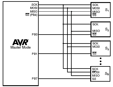
Most of the AVR MCUs have hardware support for Serial Peripheral Interface (SPI) which is a three-wire, synchronous, serial protocol. The three wires are master-out-slave-in (MOSI), master-in-slave-out (MISO), and clock. If you are going to dynamically select which device will be the master, then there is a fourth wire, slave-select (SS) which must be used. If you are using the SPI for controlling multiple peripherals then usually the Mega will be the only master and all the peripherals will be slaves. If you are using the SPI for MCU to MCU communication then usually only one MCU will be master, but using the SS line can modify this. SPI is a byte-oriented transfer with the master and a selected slave exchanging a byte simultaneously (see below). The Mega644 has one SPI interface, which is shared with the programmer. The share means that you have to be careful when attaching SPI devices so that the SPI device and the programmer never write to the interface at the same time. In practice, this means putting a resistor, perhaps 1K, between the MCU and the SPI device.
Note that the Mega1284 has two additional SPI interfaces, accessed by putting either of the two USARTs into MSPIM mode. This mode is SPI master only and, of course, the rs232 function of the USART is disabled.
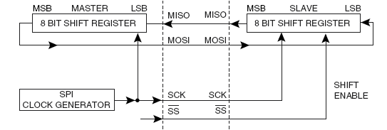
The clock rate is selectable and can be as high as 1/2 the crystal frequency when the MCU is master and 1/4 the crystal frequency when the MCU is slave. Many peripheral devices must run slower than this, however. The MCU data sheet will show how to set up registers, but Atmel appnote AVR151 explains the system more completely. As shown below, more SPI peripherials could be added by sharing the MISO, MOSI, and SCLK lines and by having a separate chip select line for each one. If the peripherals are of different type (e.g. ADC and DAC) or speed, you may need to change the SPCR settings between transfers to different peripherals.
SPI is one of serveral industry-sponsored serial interfaces which are in use. A good summary of SPI and other serial board-level protocols are at Microcontroller Pros Corp web site particularly part1, part2.
Mega32 codevision routines are here.
Using SPI in GCC
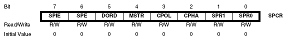
You need to set up the SPI control register, SPCR, and one bit of the status register, SPSR. The bits of the SPCR are shown below. You do not need to turn on the SPI interrupt (SPIE bit) because sending a byte is faster than getting into an ISR. You need to set SPE which enables the SPI subsystem, choose the data order (DORD), set the MSTR bit to make the MCU an SPI master, choose the clock polarity (CPOL), phase (CPHA), and rate (SPR1 and SPR0). Some rates require that you also set bit zero in the SPSR. The data order, clock polarity, phase and rate will depend in detail upon which peripheral device you are trying to communicate with. Most of the bits in the SPCR are easy to understand, but getting the clock polarity and clock phase correct may take some experimentation if the peripheral device data sheet is vague. If you are setting up SPI between two MCUs, just set the clock polarity and phase to be the same on both MCUs.
Reading and writing the SPI data register (SPDR) actually sends/receives data. See examples in the next sections.
External ADC using ADC0832
The ADC0832 is a two channel, 8-bit ADC. The input channel is set with one SPI byte transfer, then the ADC value is read with the next SPI byte transfer. The data sheet suggests that the last three bits of the input byte set the channel (start bit, mode bit, channel bit) but due to a 1 bit delay for mux settling, the input byte has to be sent (msb first) as [0 0 0 0 1 mode chan 0] with the extra zero padding the end. The mode is 1 if single-ended or 0 if differential and chan is either 0 or 1. The start bit is part of the ADC protocol, but not part of the SPI transfer protocol. The start bit is included because different members of this ADC family have different numbers of mux bits. The clock polarity and phase are set to 1 for this device. Setting the clock rate to Fosc/32 (with Fosc=16 MHz) produced a reliable conversion in about 32 microseconds. Conversion is started when the chip select line (CS) is taken low by the MCU and ends when it is taken high. Each new conversion must start with a high-to-low transition on the CS. The code shows how to set up the various i/o lines. Note also that the byte received during the mux setup is discarded in the junk variable and that something has to be sent when reading the ADC (junk in the code). Connections are shown in the table below. As always, you should put a 0.1 μfarad capacitor from Vcc to ground very close to the ADC.
| Mega644 |
ADC0832 |
| MOSI (B.5) |
DI |
| MISO (B.6) |
DO |
| SCLK (B.7) |
CLK |
| B.4 |
CS |
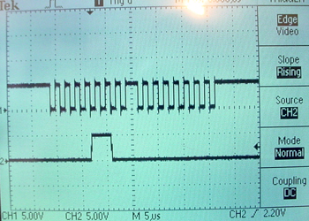
The first image below shows the CLK and DI lines with the mux setting for single-ended, channel zero. The second shows the CLK and DO lines while the ADC was transmitting the level 13. You can see that the mux command from the MCU occurs during the first eight CLK transitions, while the data is transmitted back to the MCU during the second eight.
External DAC using AD7303
The AD7303 is a two channel, 8-bit DAC with buffered voltage output. The channels may be updated simultaneously or separately. Each channel write requires two one-byte transfers to the DAC. The first is a control byte, and the second is the channel data byte. The control byte specifies which channel will be updated as well as the update mode (see larger table below). Connections are shown in the table below. As always, you should put a 0.1 μfarad capacitor from Vcc to ground very close to the DAC.
| Mega644 |
AD7303 |
| MOSI (B.5) |
DIN |
| SCLK (B.7) |
SCLK |
| B.4 |
SYNC |
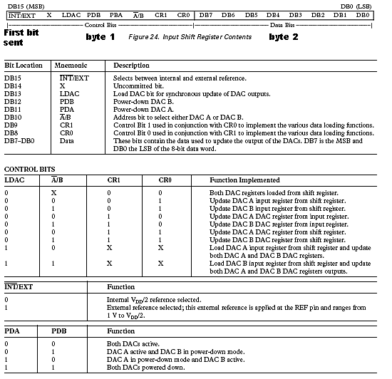
The demo program sends 4 bytes per loop to update both channels. First channel A is set up and loaded (without update), then channel B is set up and loaded, while specifiying simultaneous channel update. A table of the DAC control options is below. One control word can load channel A or B, update channel A or B, or load channel A or B and update both simutaneously. You must also specify internal or external reference voltage in each control word. If you specify internal reference, the output voltage range is 0 to Vcc.
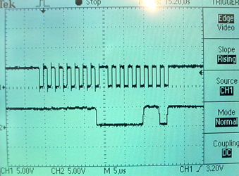
The image below shows both output channels (A on top, B on bottom). Running at 8 MHz SPI clock rate (1 microSec/byte), both channels were updated in about 5.5 microseconds. Normally, you would put the channel update code in an ISR to produce a known rate.

Copyright Cornell University Feb 2009