Overall structure of the FPGA
The FPGA floor plan shows the overall layout of the generic Cyclone5.
Our FPGA has:
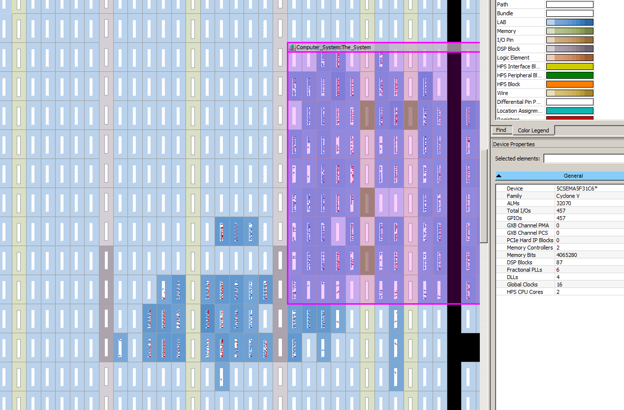
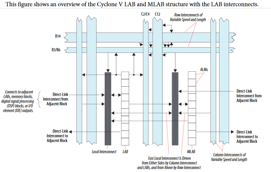
A floor plan shows that the computational fabric is arranged as a column structure, with the HPS in one corner, and I/O along the edges of the FPGA. The column structure mixes LABs, DSP, and M10k memory for fast, hopefully efficient, routing. Another view of the fabric is a screen dump from the Quartus chip planner which shows the column structure color coded for block type. Pale blue for unused ALMs, dark blue for ALMs in use. Tan for DSP and Green for memory. Zooming in to one column of the LAB structure shows some of the interconnect structure which connects ALMs within a LAB and connections between LABs.
Wiring and routing
Each LAB can drive 30 ALMs through fast-local and direct-link interconnects. Ten ALMs are in any given LAB and ten ALMs are in each of the adjacent LABs.The local interconnect can drive ALMs in the same LAB using column and row interconnects and ALMoutputs in the same LAB. Neighboring LABs, MLABs, M10K blocks, or digital signal processing (DSP) blocks from the left or right can also drive the LAB’s local interconnect using the direct link connection. Longer distance connections are handled by row/column connects which trade off speed and distance.
ALM -- Adaptive Logic Module
Each ALM can be configured in several ways.
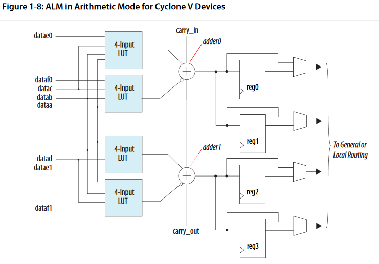
A diagram summarizing the ALM, and more ALM Detail.
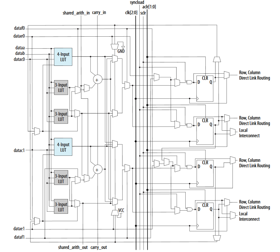
A specific ALM configuration dumped from the Quartus Chip planner interface: Detail example.
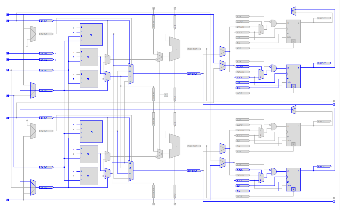
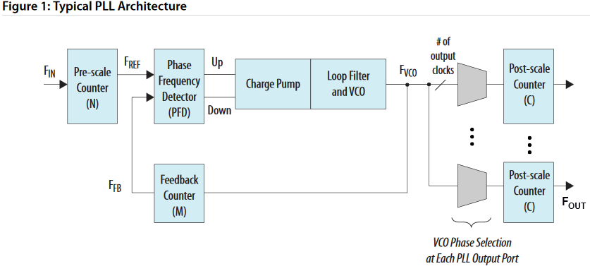
Clock Networks
The Cyclone V devices contain the following clock networks that are organized into a hierarchical structure:
Every GCLK, RCLK, and PCLK network has its own clock control block. The control block provides the following features:
• Clock source selection (dynamic selection available only for GCLKs)
• Global clock multiplexing
• Clock power down (static or dynamic clock enable or disable available only for GCLKs and RCLKs)
In Cyclone V devices, clock input pins, PLL outputs, high-speed serial interface (HSSI) outputs, and internal logic can drive the GCLK, RCLK, and PCLK networks. The clock networks attempt to deliver minimum clock-skew signals by using a distribution tree.
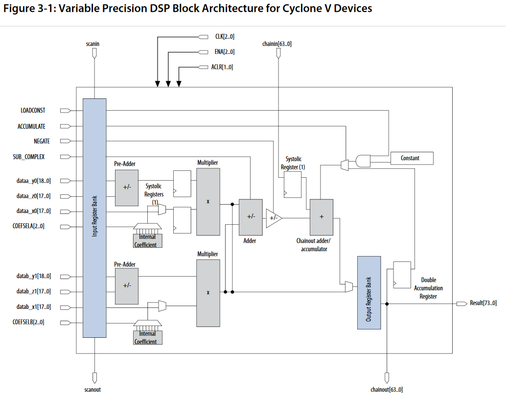
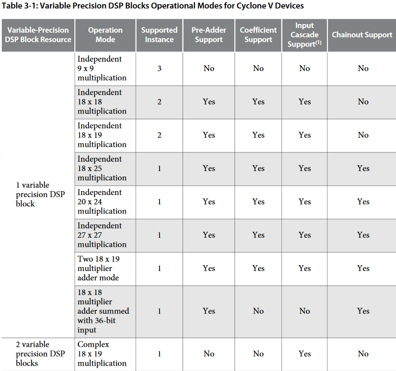
DSP
The Cyclone V variable precision DSP blocks offer the following features:
• High-performance, power-optimized, and fully registered multiplication operations
• 9-bit, 18-bit, and 27-bit word lengths
• Two 18 x 19 complex multiplications at a rate of 250 MHz.
• Built-in addition, subtraction, and dual 64-bit accumulation unit to combine multiplication results
• Cascading 19-bit or 27-bit to form the tap-delay line for filtering applications
• Hard pre-adder supported in 19-bit, and 27-bit mode for symmetric filters
• Internal coefficient register bank for filter implementation
• 18-bit and 27-bit systolic finite impulse response (FIR) filters with distributed output adder
The DSP blocks seem quite complex to set up, once you get past simple multipication. Some functions can be inferred from Verilog (see page 13-5 of HDL styles), but you should look at the DSP summary document, and consider using the Quartus IP modules LPM_MULT, ALTERA_MULT_ADD, ALTMULT_COMPLEX to infer DSP blocks.
The Cyclone V variable precision DSP block consists of the following elements:
• Input register bank
The input register bank consists of data, dynamic control signals, and two sets of delay registers. All the registers in the DSP blocks are positive-edge triggered and cleared on power up. Each multiplier operand can feed an input register or a multiplier directly, bypassing the input registers.
• Pre-adder
Each variable precision DSP block has two 19-bit pre-adders. You can configure these pre-adders in thefollowing configurations:
-- Two independent 19-bit pre-adders
--
One 27-bit pre-adder
The pre-adder supports both addition and subtraction in the following input configurations:•
--
18-bit (signed) addition or subtraction for 18 x 19 mode•
--
17-bit (unsigned) addition or subtraction for 18 x 19 mode•
--
26-bit addition or subtraction for 27 x 27 mode
• Internal coefficients (two banks of 8 coefficients)
The DSP block has the flexibility of selecting the multiplicand from eitherthe dynamic input or the internal coefficient.The internal coefficient can support up to eight constant coefficients for the multiplicands in 18-bit and 27-bit modes. When you enable the internal coefficient feature, COEFSELA/COEFSELB are used to control the selection of the coefficient multiplexer.
• Multipliers
One 27 x 27 multiplier, or Two 18 (signed)/(unsigned) x 19 (signed) multipliers, or Three 9 x 9 multipliers
• Adder
You can use the adder in various sizes, depending on the operational mode:
--
One 64-bit adder with the 64-bit accumulator
--
Two 18 x 19 modes—the adder is divided into two 37-bit adders to produce the full 37-bit result ofeach independent 18 x 19 multiplication
--
Three 9 x 9 modes— you can use the adder as three 18-bit adders to produce three 9 x 9 multiplicationresults independently
• Accumulator and chainout adder
• Systolic registers
If the variable precision DSP block is not configured in systolic FIR mode, both systolic registers are bypassed.
• Double accumulation register
• Output register bank
FPGA I/O
The Cyclone V I/Os support the following features:
• Single-ended, non-voltage-referenced, and voltage-referenced I/O standards
• Low-voltage differential signaling (LVDS), RSDS, mini-LVDS, HSTL, HSUL, and SSTL I/O standards
• Serializer/deserializer (SERDES)
• Programmable output current strength
• Programmable slew-rate
• Programmable bus-hold
• Programmable pull-up resistor
• Programmable pre-emphasis
• Programmable I/O delay
• Programmable voltage output differential (VOD)
• Open-drain output
• On-chip series termination (RS OCT) with and without calibration
• On-chip parallel termination (RT OCT)
• On-chip differential termination (RD OCT)
• High-speed differential I/O support
Cyclone 5 FPGA memory
The memory systems of Altera Cyclone5 FPGAs have various features and limitations.
I will not talk about the HPS side here, only the FPGA side.
Memory systems include:
See also: