Charles HY Cheung, Fall 2007,
Abstract
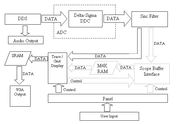
High Level Design
The bitstream output of the DDC signal is fed into the sinc filter, which filters and decimates the signal to a 16-bit word. The effective max sample rate is thus reduced to the Nyquist 20MSps/(decimation rate * 2). The decimated signal is fed into a controlled buffer. The controlled (oscilloscope) buffer fills up M4K RAM based on specified trigger parameters. When triggered or held, the oscilloscope will stop acquiring. Due to the difficulty of synchronizing M4K RAM to the VGA trace, a buffered signal display was never realized. Hence, the decimated signal is fed into the trace display for direct tracing of the signal instead.
The trace display writes the VGA-mapped SRAM and reads the user-specified control parameters to generate a grid, the vertical voltsperdiv amplitude, and the secperdiv speed of the trace. Bypassing the difficulties of floating point operations in hardware, these values were represented differently as a division factor of the maximum amplitude and as a division factor of the drawing speed. Because a quantized number of pixels are displayed on the screen, the speed of the trace is directly related to the acquisition speed of the decimated signal.
The panel is used to interface user input, such as the switches on the DE2 dev board, with control values.
Program Hardware Design
An analog signal generated by a direct-digital synthesizer lookup table is fed into the DDC. An ADC delta-sigma converter consists of a negative feedback impulse generated by a comparator fed in with the signal into an integrator. The resultant output is a series of pulses that vary in period with the input signal level. In order to model this digitally, a delta-sigma DDC was used. The integrator was modeled by a latched adder followed by a most significant bit comparator. The bitstream is converted to 2’s complement to match the output signal of the audio DAC.
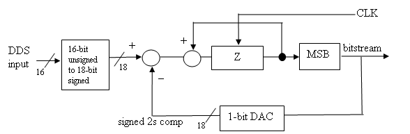
Z is a clocked delay. CLK is the acquisition rate of the DDC.
Sinc Filter
A 24-bit IIR 3rd order Sinc filter was modeled based on the AD7401 datasheet. The topology shown below consists of an accumulator followed by a differentiator. A decimation rate control value was added into the Sinc filter to allow user variation of effective sampling speed, which is equivalent to the ADC sample rate / decimation rate. A larger decimation value would allow a greater time capture of the incoming bitstream, allowing for greater accuracy trading off acquisition speed. The AD7401 Datasheet describes the signal gain to decimation rate.
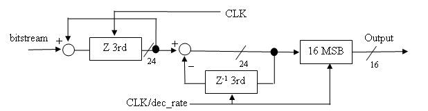
Z is a clock delay. Z-1 denotes a prior delay at clock.
Scope Buffer Interface
The scope buffer interface is used to write the decimated signal into RAM at a specified rate. It supports triggering to stop writing at either a rising or falling edge of a specified threshold. It also detects when it’s full and has a hold input to stop writing. This allows for very long pipelined history of the trace to be viewed.
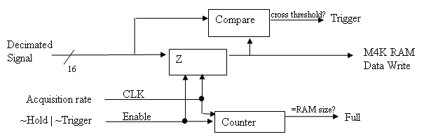
Z is a clock delay. Counter is cleared after RAM size is reached.
Trace Display
The trace display module is a state machine that updates the grid and trace on the VGA based on control values. The grid has a maximum of 10 horizontal and vertical divisions that are specified for the 640x480 VGA display depending on the viewport size. The trace pixels are quantized by scaling the size of the decimated signal. The trace is drawn until the end of the screen is reached. Once the end is reached, the trace is redrawn from the left to the right. An alternative pipeline mode was used to display the history of the trace by viewing what was in M4K RAM. Since the M4K ram did not synchronize with the VGA, it was discarded.
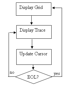
Simplified Flow Chart of
The y-coordinates of the trace is determined by the formula:
TRACE_POSITION = (INPUT*YVIEWPORTRES)/(32'hFFFF+volperdivval) + OFFSET
where the 16-bit INPUT signal is scaled down to the specified viewport resolution. The scaling happens at maximum viewport resolution so an additional term volperdivval when increased decreases scope’s Vref/Div value.
The speed of the trace is divided by the screen blanking rate by the term secperdivctr which is the dividing factor. For the 640x480 screen, the vertical and horizontal syncs at an average of 4 pixels drawn which happens at
TRACE_SPEED = VGA_CLOCK / [(VSYNC|HSYNC)
* STATES * secperdivctr] = 25.2MHz / [4 * 3 * secperdivctr]
Being a dividing factor, secperdivctr is inversely proportional to actual Sec/Div and is given approximately by
SEC_PER_DIV =
PIXELS_PER_DIV / TRACE_SPEED
For a viewport that spans the whole 640x480 screen and with a grid of 10 divisions, there are 64 pixels per div.
Results & Conclusions
|
|
Min |
Max |
|
Input Signal Speed |
0.1 Hz |
1.25 MHz |
|
Vref/Div |
0.00416 |
0.2 |
|
Sec/Div |
30 μs |
1 s |
Assuming a grid of 10 x 10 divisions at 640x480 resolution
The maximum input signal speed would result in an 8-bit resolution, which is adequate for a maximum of 256 pixel y-resolution. Any further speeds will reduce the resolution to 20MHz / (decimation rate – 8). The minimum input signal speed is limited by the Sec/Div resolution. Assuming a whole period needs to fit on the screen, 1/10s = 0.1Hz. Note that slower frequencies can be viewed but the period would not fit in one trace drawing.
Vref is the maximum reference voltage value which, for the DDS, is a 2s complement number. With the real-world size of the viewing display, the actual Vref/Div is decreased. An amplifier is included in the code to increase the Vref/Div range, however, bit size will have to be increased for all ADC stages, as well as the trace and buffer. Maximum Vref/Div is thus constrained by word size, which can be changed. For real hardware, a DAC controlled analog amplifier or chain of amplifiers is best with a specific rail range. Typically this is in the tens of volts. One must choose an amplifier with an appropriate bandwidth to handle maximum input signal speeds. For the AD7401 ADC, suggestions are made in the datasheet.
Maximum Sec/Div is limited by secperdivctr bit size, which is at 21 bits. It is trivial to increase this size for very low frequency readings.
Minimum Sec/Div is limited by the VGA vertical and horizontal sync rate, as well as the number of states drawn. If the M4K RAM was implemented successfully, this value could be lowered to the maximum input signal speed or beyond.
Project Constraints
As aforementioned, the initial constraint on the analog side was the package size of the chip, limited by the SOIC process with minimum 1mm spacing between leads. Although it’s possible to solder SOP chips with the use of solder paste, flux, and steady hands, a lack of experience and the need for simple hardware dissuaded the use of SOP chips, although they will be revisited for further improvements. The primary constraint in the digital part of the project was the M4K RAM not synchronizing with the horizontal and vertical sync of the display. A rasterizer component clocked to the refresh rate of the VGA can possibly alleviate these issues since it provides a layer between the controlling trace and SRAM. Clock synchronization is important in scope display to display real-time changes as soon as they happen to the viewing signal.
Once a proper rasterizer is complete, the trace history can be read and the next step would be to implement a scrolling trace. Afterwards, work would be done to maximize the capturing pipeline to view a large time history of a signal. Also, the addition of equivalent time sampling techniques can allow reading of faster periodic input signal speeds.
Another important DSO function is the ability to store data. Development time would be decreased since the flash SD Card interface is already written for the DE2 Board.
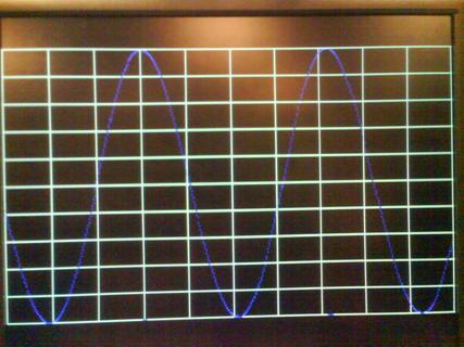
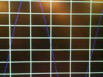
A slow trace at 16 Hz, at ~15mSec/Div, 0.2 Vref/Div, is shown below:
Appendix
http://www.qsl.net/wd1v/scopefaq/
DSO FAQ
http://www.analog.com/UploadedFiles/Data_Sheets/AD7401.pdf
Analog Devices AD7401 Datasheet
Interfacing the Nintendo DS with a FPGA
Abstract
In order to add extended functionality to the DE2 Dev board, the Nintendo DS could be interfaced through the Slot-1 connector through GPIO. The benefit of interfacing a FPGA to the DS is the capture and use of the touch screen, dual 3” TFT 256 x 192 displays, 802.11b Wi-fi, microphone, and stereo audio output. More importantly, the ubiquity and portability of the system can allow FPGA projects to be redesigned into a Slot-1 PCB for portable projects at low cost. The initial proposed idea was to implement the graphics of the oscilloscope on the DS so that the device could be made portable.
DS Hardware
The Nintendo DS hardware is well-documented from the
homebrew scene. It consists of an ARM7
and ARM9 processor at speeds 33 MHz and 67MHz respectively. More importantly, the Nintendo DS cartridge,
or what is known as the Slot-1 cart, contains program code flashed to ROM that
the DS initializes and runs from. The
cart is the subject of a possible method to allow communication between the
FPGA and the DS at ARM7/ARM9 program instruction speed.
DS Slot-1 Connection
The physical I/O pins of the slot-1
connection is shown below:
|
Pin |
Function |
|
1 |
GND |
|
2 |
CLK (active high) |
|
3 |
NC |
|
4 |
ROM CS (selects when low) |
|
5 |
ROM reset |
|
6 |
EEPROM CS (selects when low) |
|
7 |
GND (IRQ removal detect) |
|
8 |
+3.3V |
|
9 |
D0 |
|
10 |
D1 |
|
11 |
D2 |
|
12 |
D3 |
|
13 |
D4 |
|
14 |
D5 |
|
15 |
D6 / MISO |
|
16 |
D7 / MOSI |
|
17 |
GND |
where D0-D7 are the 8-bit ROM lines.
The EEPROM SPI signal is sent over a data lines MISO MOSI a clock after CS is set to low. The handling of the SPI data must be performed by either the Slot-2 or Slot-1 ROM instruction data. The SPI that the Slot-1 connection employs uses a phase and polarity of 1, WCOL and ROE set to 1.
Method
Since a SPI module is included in SOPC Builder, it is trivial to include 3 SPI pins through GPIO. The problem with this is the baudrate limit of 2MHz. Although not affecting the current project’s scope limitations, this idea was initially rejected because of its slow speed. In addition, the use of Slot-1 ROM for program instruction would have the FPGA employ a switching scheme in which ROM CS is set high and EEPROM CS set low to enable the external SPI. This requires a hex file header with the proper registers to bypass encryption and load compiled ARM7/ARM9 data into the ROM data lines of the DS. Thinking along these lines, it’s possible to have maximum program instruction speed for data transfer, which means a speed of 67MHz, discounting the processor cycle per VGA instruction which will lower this rate.
The proposed scheme follows these steps:
- Set ROM CS low to enable ROM data reads
- Transfer a header file that bypasses encryption
- Upon the DS requesting the bypass data address, send a compiled DS hex code which initializes on the ARM7/ARM9 processor
- The DS hex code, for example, will have an infinite loop to draw x and y pixels at a certain color, or will buffer in data for a trace.
- Upon receiving a specific OPCODE command, the x and y pixels with the color, or trace data, will be replaced by the FPGA in hardware.
Hence a DS VGA driver or FPGA ARM7/ARM9 data transfer scheme can be written in Verilog for this purpose. In fact, almost all functions of the DS are exploitable as long as the Verilog can synchronize to the specific OPCODE command.
Compiling DS hex code for ARM7/ARM9 program instruction is already well established in the homebrew community. See PALib, DevKitPro, libnds.
References
http://neimod.com/dstek/ ARM7 and ARM9 I/O registers
http://www.natrium42.com/wiki/Main_Page DS serial documentation - A device that communicates through SPI.
Requires a Slot-2 Flashcard for implementation.
http://nocash.emubase.de/gbatek.htm A
comprehensive list of memory maps, I/O registers, and other related info.
Includes header information to bypass encryption.
http://masscat.afraid.org/ninds/serial_files/doxygen/index.html
SPI/UART Bridge driver
http://files.darkfader.net/ds/files/cartridge.txt
DS Slot1 Pinout
http://www.palib.info/ PAlib
http://www.devkitpro.org/ DevKitPro – IDE & libraries for compiling DS ARM7/ARM9 code. Libnds as well as PAlib is included.