*Note: This website is an eye-friendly technical website and so is display in high contrast. Click here for a more normal view.
Introduction
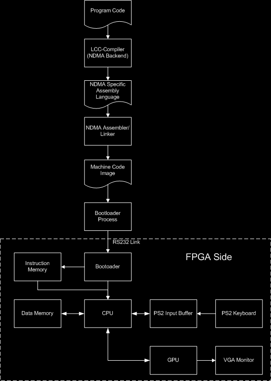
Design of a fully integrated toolkit for system generationThis project was the design of a software and hardware toolkit for the purpose of implementing a fully featured system on chip computer. This required the accurate design of all the different sub systems and architectural systems that had to be put together to get a program running on such a system. Below is a diagram of a demo configuration of the system which supports user input through a PS2 keyboard and output through a VGA monitor.
High Level Design
Rationale
The rationale of this project oriented around being able to create a complete system on chip through the use of a set of modules combined in what I call a toolkit. A large motivation was due to Object Oriented Design from computer science where functional elements are written once and reused. Once the interfaces are established it is easy to swap out different modules and write different modules for different applications
This was done here through an asynchronous handshake interface which allowed any amount of data to be transferred between two modules that could be on different clock domains. This is very prevalent with the demo setup since all the different hardware modules are running at very different speeds.
The best part about this toolkit is that it can be simply "cut and pasted" into a design for the purpose of rapid prototyping. It is extremely useful for debugging since unlike similar tools like Altera's SOPC builder the code is open and available to view. This can be used to debug through hardware logic analyzer tools or with simulation tools such as Icarus Verilog.
Logical Structure
The logical structure of this project is shown above in the overall state diagram so it will not be repeated here. To briefly explain, each of modules on the FPGA side were written and tested in Verilog while the other systems are written in C++ on Window's Visual Studio 2005.
The core architecture was a custom RISC architecture called NDMA or Network Driven Microprocessor Architecure where the assembler implemented these instructions from assembly language. The NDMA compiler used was LCC which allowed me to plug in a custom back-end to an already pre-made and tested compiler front end but all the while having it produce code for my custom architecture.
Hardware/Software Tradeoffs
In this design a few design decisions were made to simplyfy either the hardware or the software where the other option represented a large jump in complexity. For example the NDMA Architecture implemented single cycle branches and loads through the use of overlapped execution and a dedicated data memory. This was for the purpose of decreasing the size of code and ensuring that timing was exact for network operations. However, has the downside of having to load program resources at program runtime.
The Altera M4K blocks which were used for data memory did not support unaligned memory access so instructions such as:
Could not be implemented without the implementation of compiler complexity. So to counteract this the data memory used was set as a 32 bit wide location and software complexity implemented so that characters are given a memory location each. This is an inefficiency of the architecture due to the deficiency of the memory blocks. A future module to implement would be a 4 m4k block array of 8 bit words. However, time is always a factor in a design and this will be done in the future.
Standards
The toolkit contains modules which interface with a wide variety of standars.
- The Bootloader uses the RS232
standard which is an asynchronous serial communications protocol.
- The GPU implements a VGA signal interface, however the standard was implemented
by a VGA controller module and PLL which were not written by me rather but are modified
versions of default Altera code.
- The PS2 Input Buffer implements the PS/2 Keyboard interface standard with scan
code set 2. The PS/2 interface is also essentially a serial interface although is not
asynchronous since the keyboard provides a clock.
- The NDMA cpu was originally based on the mips encoding of instructions and
their op codes however many have changed substantially and it does not conform to the
MIPS standard in most ways anymore.
- The LCD Module implements the HD44780 LCD Standard for interfacing with the
LCD on the DE2 Board. Although I never plugged this into an output buffer this
could be done using my interfacing standard that I implemented.
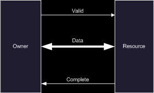
My Interface Standard - I implemented my own standard that allowed different modules of different clock domains to interface. Essentially the interface consists of a two wire handshake. The owner of the resource will have an output valid signal and an input complete signal where the resource will take the valid as input and output the complete. When the owner would like to "activate" the device it will set the data and set the valid line high. When the resource is done it will set the complete line high which the owner will then use to lower the valid flag thereby resetting the resource. Similarily if the owner would like to recieve the resource the same thing is done except the resource would set the data the owner would read it in and only afterwards the valid line would go low.
Patent/Trademark Information
The DE2_TOP.v file provided by Terasic was used as the base of design for the top level module of the design which essentially is the place were all the connections for the system were made. Most of this file is simply declarations for the purpose of connecting the Cyclone II FPGA to the DE2 board and is not pertinent to the contents of my project. However, this file does demonstrate some of the basic logic required to ensure correct functionality of the project.
Also the GPU contains a VGA controller logic that was not written by me. These files consist of the VGA controller logic except for the VGACNT module which was written to encapsulate their function. The VGA controller code was bundled with the DE2 default code put on the CD-rom received with the system.
Design
Hardware
This project involved the design of a variety of different hardware modules of varying functionlity. They all follow the appropriate interfacing standards to interface with peripherals or with other modules.
Network Driven Microprocessor Architecture CPU
The NDMA cpu core is designed based on the instruction encoding scheme of MIPS but this is where most of the similarities lie. The CPU is an overlapped execution CPU where the PC is incremented on the negative edge of the clock, which will then make all of the values of the current instruction valid by the next negative when the register file is written to. The advantage, however, is that on the positive edge the quick compare result and ALU results will be valid so that the PC will be incremented to the right spot without need of a branch delay. Also the load needs no delay due to a dedicated data memory which cost is offset in software complexity. This allows for a very close to completely RISC architecture ideal for network based multiprocesser mesh networks.
The CPU uses a dedicated in/out register module which is used to interface the CPU with outside modules. Also the architecure contains instructions for the purpose of network driven operation but this has been disabled for the current project and will be enabled in the near future.
Below is a table listing all of the supported instructions for the CPU. This demo CPU does not have a multiply enabled however it is written into the verilog code and could be enabled. Since the FPGA has dedicated multiplys this would meet the timing requirements (however the divide does not so it is suggested not to enable this unit but rather in the future add a dedicated mult/div unit which will halt the CPU until done.
| Instruction | Instruction Status | |
| Memory Operations | ||
| lw | Load Word | yes |
| lh | Load half word | yes |
| lhu | Load half word unsigned | yes |
| lb | Load byte | yes |
| lbu | Load byte unsigned | yes |
| sw | Store word | yes |
| sh | Store half word | yes |
| sb | Store byte | yes |
| Immediate Ops | ||
| addi | Add immediate | yes |
| addiu | Add immediate unsigned | yes |
| lui | Load upper immediate | yes |
| slti | Set less than immediate | yes |
| sltiu | Set less than immediate unsigned | yes |
| andi | And immediate | yes |
| xori | Exclusive OR immediate | yes |
| ori | OR immediate | yes |
| smsg | Send message to CPU | yes |
| rmsg | Receive message from CPU | some |
| sid | Set processor ID | yes |
| Register Instructions | ||
| add | Register add | yes |
| addu | Unsigned register add | yes |
| sub | Register subtract | yes |
| subu | Unsigned register substract | yes |
| and | Register AND | yes |
| or | Register OR | yes |
| xor | Register XOR | yes |
| slt | Register set less than | yes |
| sltu | Unsigned register set less than | yes |
| sll | Shift left logical | yes |
| srl | Shift right logical | yes |
| sra | Shift right arithmetic | yes |
| Branch Instructions | ||
| bne | Branch on not equal | yes |
| beq | Branch on equal | yes |
| bgtz | Branch on greater than zero | yes |
| bgez | Branch on greater than or equal to zero | yes |
| bltz | Branch on less than zero | yes |
| blez | Branch on less than or equal to zero | yes |
| j | Jump | yes |
| jal | Jump and link | yes |
| jr | Jump to register | yes |
| In / Out Instructions | ||
| in | Read input from port | yes |
| outi | Output immedaite to port | yes |
| out | Output register to port | yes |
| Mult/Div/Mod | ||
| mult | Register multiply | yes, but disabled |
| multu | Unsigned register multiply | yes, but disabled |
| div | Register divide | yes, but disabled |
| divu | Unsigned register divide | yes, but disabled |
| mod | Register modulus | yes, but disabled |
| Control Operations | ||
| nop | No Operation | yes |
| break | Temporary Break | yes |
A Note on using the in/out instructions. The in/out instructions are used in the following manner:
outi $destination, immediate
in $destination, $source
The destination register in the OUT commands is the appropriate output
port (where $5 --> portE) and the source is a CPU register. For the IN
commands the source is from the input port and the destination is a cpu
port. Notice that IN can be used to read an output port but out can only
be used to write to an output port.
The ports in the current design are PortA-H --> $1-8. So this means that
OUT can only be applied to output registers $5-8.
GPU
The GPU module is essentially a small processor which takes inputs from the CPU on a CPU output port. The GPU is capable of drawing lines, plotting pixels, or drawing ASCII text to the screen.


A sample connection to the CPU is as follows:
Input PortA[0] <== GPU Complete Flag
Output Port E[15:0] ==> GPU Instruction
Output Port E[16] ==> GPU Valid Flag
The way that the GPU receives instructions is on the GPU instruction line which is of format:
GPUInstruction[15:10] - Operation
GPUInstruction[9:0] - Data
The possible operations to the GPU are as follows:
| Instruction | Encoding | Description |
| setX1 | 000000 | Sets the internal X1 register to data[9:0] |
| setY1 | 000001 | Sets the internal Y1 register to data[9:0] |
| setX2 | 000010 | Sets the internal X2 register to data[9:0] |
| setY2 | 000011 | Sets the internal Y2 register to data[9:0] |
| setChar | 000100 | Sets internal char register to data[7:0] |
| drawChar | 000101 | Dispatches a char to the ASCII module with color data[7:0] |
| drawLine | 000110 | Dispatches the internal registers to the Bresenham module with color data[7:0] |
| drawPixel | 000111 | Dispatches internal registers to pixel plotter with color data[7:0] |
| clear | 001000 | Resets the SRAM screen buffer to 0 |
PS2 Buffer
The PS2 input buffer is designed in much the same way as the other modules implementing the same communication interface. The module will poll the PS2 port and receive information on it. When a valid key is pressed it will write this key into it's buffer and increment a write pointer which will mismatch with the write pointer and indicate that the buffer is now not empty.
This output is oBufferEmpty and is not quite in line with the protocol but since this is just an indicator flag it is not a problem. The CPU can then use this flag to check if there is a character pending and then use the interface talked about before to read in the next character one at a time. Every time a character is read the valid flag must be lowered before the next character can be read. This is to ensure that no characters are lost.
A sample connection of the PS2 Buffer to the CPU is as follows:
Output Port F[0] ==> Valid
Input Port B[9] <== Buffer Empty
Input Port B[8] <== Complete
Input Port B[7:0] <== ASCII
RS232 Buffer
The RS232 input buffer is exacltly like the PS2 input buffer except it writes into the buffer from input on the RS232 port and also allows to transmit out on the RS232. To read it is exactly the same as the PS2 so I will talk about transmitting. To do this it implements the same interface as all the other modules. The CPU can set up a data value on the ASCII transmit data line and then set the valid high, when the value has finished transmitting the complete will go high and the module can be reset.
Bootloader
The bootloader module is a giant state machine which uses the RS232 input buffer to communicate with a host computer to receive and bootload a program on the RS232 line. This is extremely useful to bootload any kind of memory as long as the memory is written using a standard memory interface.


The bootloader will output a signal oBootload which will say that the bootloader is bootloading. This is useful as a CPU reset or to tell whatever circuit is using the bootloader that the bootloader is the current owner of the connected memory.
The way that the bootloader knows there is a want to bootload it is by waiting for an input on the RS232 and checking to see if it gets the string "boot". If this is the case it will transmit back "ready" to signal the caller it is ready to receive a program. At this point the oBootLoad output will go high. The bootloader will then proceed to receive a 32 bit address value and return it for verification and then receive a 32 bit data value and retrun transmit it for verification. It will then write the 32 bit data value to the 32 bit address value. Once done it will return to the receieve address state and repeat the process until a 0xFFFFFFFF is received as the next PC. This is considered a bootload break message and the bootloader will go back to the initial state.


note: The actual states are not as shown above. The state machine has 2 states for each receive and each transmit. That means 8 states for receive "boot", 10 states for transmit "ready", and another 4 states for each address and data receive/transmit. Also it requires a few states for the memory operations and some other logic. The real state machine contains 30 states. Many states were preferrable fewer states and counters since counters are harder to debug and essentially are state machines in their own right.
Other Modules
This project contains a number of other modules that are used in the above modules or have been developed and can be used as a part of this toolkit:
| APU | Audio Processor Unit | This is an audio synthesis module which will allow a program to generate tones and output it to the AUDIO DAC on the DE2 board. Some of the code in this module is not original and was taken from the DE2 default code. The processor unit side of it, however, was written. |
| LCD | LCD Controller | This module will take a memory as an input and write this out to the LCD display on the DE2 board. This is useful as an output buffer however an output buffer module has not been written. It would be easy to implement the common interface of this project and design one since it would be wholly a memory oriented module. |
| Memory | M4K, SRAM | A few modules were written to abstract the creating on M4K block based memories of single and dual port. Also an SRAM memory module was created and an SRAM Screen Buffer which is used in the GPU. |
Software
Compiler
The compiler used was LCC which is a retargetable ANSI compatible C compiler. The back-end was written such that the assembly language the compiler generated was specific to the NDMA architecture and would interface cleanly with the assembler.
Since LCC does not support any asm( ) commands the rcc aspect was used which spat out the assembly. This was used to generate the assembly code and then cut and paste into a bigger assembly file which included other functions implemented in assembly. This was important since all input and output functions had to be aritten in assembly for compactness and the ability to access the in/out/outi instructions.
To write the back end an NDMA lburg file was written which explains to the compiler how to convert the lexical symbols into interpretted assembly code. This file was heavily modified from a pre-existing example provided with LCC since much of the contents in the file are specific to LCC or general for all architectures and did not need to be changed. Much of the file was altered, however, to work with the NDMA architecture.
A significant point to be made about the lburg file is that the compiler was used to offset the issue of data words being 32 bits. When manipulating strings the compiler was programmed to jump to a snippet of code the compiler generated in the assembler through a .byte directive and run that code. This code would temporarily store the string into data memory at a known location that was saved. The snippet would return and the code then packed into a register so that on the CPU a character would not waste registers. Then when saved back into memory the data was once again unpacked. This incurred a substantial penalty involving code length but it was the most eloquent solution.
Usage
To use the compiler it must be built. To do so you must run the following
in a Visual Studio 2005 build window or a build enviornment which has nmake
from Visual Studio 6.0 or later:
...ProjectModules\LCC>set BUILDDIR=\lcc_build_directory
...ProjectModules\LCC>nmake -f makefile.nt all
This will build the compiler into your build directory you specified and then to compile a program you must run:
...build_dir> rcc -target=ndma/ndmaOS filename.c
This will spit out the assembly code which can then be "cut and paste" into the assembler code which should include some of the APIs as explained below. If wanted it is possible to output the rcc output to a file by doing the following:
...build_dir> rcc -target=ndma/ndmaOS filename.c > outfile
If desired the build directory can be added to the system path and you
can run this program wherever you code resides.
Assembler-Linker
The assembler-linker program is an NDMA specific assembler program. It does some basic in file linking. It does not support multiple files but will link all locations within itself. It will also parse through specific directives and pseudo instructions:
.SetStack - This will initialize the stack to a specific size (data memory size)
.Boot - This will jump to the label defined (usually main)
.byte - This will load in a specific byte into data memory
la - Load Address, this pseudo instruction has special behavior. When used in the context of a memory calculation it will simply load in the number to that specific register. However, if it is used with a label it is taken as a memory load and processed accordingly. This works in conjunction with the compiler which will use the la instruction to load memory into the CPU.
The structure of the assembler is that it first parses through the file to check for labels for linking. These labels are placed into a map data structure to be accessed later. Then the assembler parses through the assembly file as normal and inteprets the assembly instructions, directives, or pseudo instructions accordingly. The instructions are checked against a OP map data structure which is initialized at the begining of run time. The directives and pseudo instructions are checked manually since there are not many of them. However, a similar approach could be taken if more are added. The OP map is interpretted with a function that is very easily adjusted for adding instructions. If one would want to add instrutions all that is needed to do is add a OP_ to the OP enum in the BASM.h file. Then instruction must be added to InitializeOPMap() and OPFunctionSADecode(...) according to the instruction. This is very automatic for most instruction types where the type is also defined in the OPFunctionSADecode(...) function.
With this assembler that can be redefined it is possible to write a wide variety of images. This assembler was somewhat optomized using map data structures but further optomizations are possible although not important for the size of programs that would run on the NDMA processor.
Usage
To use the assembler simply run:
...ProjectModules\Software\Assembler\debug>NDMAAssembler filename.asm
The file must be an .asm file. The output will then be put into a file of the same name such as: filename.mem. This is an ASCII viewable file which would then be the input to the Bootloader. Look through this file to see which machine codes refer to what instructions. Although during the run of the assembler an output of debug messages will be displayed which may be useful in verification and debugging.
Bootloader
The bootloader will take a file from the assembler in the form of a .mem file and will bootload the CPU with it. The program needs no configuration since the baud rate of the RS232 module on the FPGA design and the program match at 115200. However, if the computer does not support this baud rate for some reason it is easily changed in the program and in the Verilog.
Usage
To run this program copy it into the directory of the assembler or the .mem file
the assembler is outputting and then run it as such:
> NDMABootloader COM# filename.mem
COM# would be the com number and used such as COM4 for the COM4 port. The filename is the name of the file you would like to bootload.
The program simply runs through the file and spits out the location and instruction on and verifies the receieve from the CPU. In the case that the recieve does not match the program will return the two mismatches, and quit. This will leave the CPU in a state where it must be restarted disallowing for strange behavior. When the program reaches the final instruction in the file it will repeat it a few times (which may not be wanted but is useful for the usual break or jr $31 instructions) and then send a 0xFFFFFFFF as the PC and wait for the reply. The reply will then confirm that the CPU has finished the bootloading process and received all of the data correctly.
GPU and PS2 APIs
Although I didn't have much time to implement much code other than testing code a few assembly based API calls:
void plotpixel(int x, int y, char color);
- Plots a pixel to location x and y.
void drawchar(int x, int y, char c, char color);
- Draws a character c to location x and y.
char getchar();
- Waits for a character to be enterred and returns it (blocking).
int waitchar();
- Returns 1 if character waiting in buffer, otherwise returns 0.
Color in form of an 8 bit char: 8'brrggbbxx
These routines are written in assembly and the function declerations are in the c code that uses them. To get them to work the routines need to be placed into the code between the .Boot main directive and the main: label. The aseembler will then link it correctly.
Example Chain
C Code
// ndmaTest0.c
int add(int in, int mul)
{
int val = in + mul;
return val;
}
void main(void)
{
int i = 0;
int j = 1;
for(i = 0; i < 5; i++)
{
j = add(j, 3);
}
}
Output from RCC
.SetStack 255
.Boot main
.text
.text
add:
addi $sp,$sp,-4
addu $24, $4, $5
sw $24,-4+4($sp)
lw $2,-4+4($sp)
L.1:
addi $sp,$sp,4
jr $31
.end add
.text
main:
addi $sp,$sp,-12
sw $23, 8($sp)
sw $30, 10($sp)
sw $31, 11($sp)
or $30, $0, $0
la $23, 1
or $30, $0, $0
L.3:
or $4, $23, $0
la $5, 3
jal add
or $23, $2, $0
L.4:
la $30, 1($30)
la $24, 5
slt $1, $30, $24
bne $1, $0, L.3
L.2:
lw $23,8($sp)
lw $25,9($sp)
lw $30,10($sp)
lw $31,11($sp)
addi $sp,$sp,12
jr $31
.end main
Output from NDMA Assembler
00110100000111010000000011111111 // ori $sp, $0, 255 (SetStack)
00001000000000000000000000001000 // .Boot main pc:8
00100011101111011111111111111100 // addi $sp, $sp, -4
00000000100001011100000000100001 // addu $24, $4, $5
10101111101110000000000000000000 // sw $24, -4+4($sp)
10001111101000100000000000000000 // lw $2, -4+4($sp)
00100011101111010000000000000100 // addi $sp, $sp, 4
00000011111000000000000000001000 // jr $31
00100011101111011111111111110100 // addi $sp, $sp, -12
10101111101101110000000000001000 // sw $23, 8($sp)
10101111101111100000000000001010 // sw $30, 10($sp)
10101111101111110000000000001011 // sw $31, 11($sp)
00000000000000001111000000100101 // or $30, $0, $0
00100100000101110000000000000001 // la $23, 1
00000000000000001111000000100101 // or $30, $0, $0
00000010111000000010000000100101 // or $4, $23, $0
00100100000001010000000000000011 // la $5, 3
00001100000000000000000000000010 // jal add (2)
00000000010000001011100000100101 // or $23, $2, $0
00100111110111100000000000000001 // la $30, 1($30)
00100100000110000000000000000101 // la $24, 5
00000011110110000000100000101010 // slt $1, $30, $24
00010100000000011111111111111001 // bne $1, $0, L.3
10001111101101110000000000001000 // lw $23, 8($sp)
10001111101110010000000000001001 // lw $25, 9($sp)
10001111101111100000000000001010 // lw $30, 10($sp)
10001111101111110000000000001011 // lw $31, 11($sp)
00100011101111010000000000001100 // addi $sp, $sp, 12
00000011111000000000000000001000 // jr $31
Results and Analysis
This lab was overall successful. The system was mostly working but would require a much longer time of testing to get all of the bugs out. Since there are so many levels at which a bug could reside testing would be required that would automate the process and find build breaks immediately. This process would be needed for an amount of time and the code meanwhile maintained. However, such is the nature of these systems and the system design has shown a high degree of success at dealing with random functions and random operation.
The CPU is being clocked a bit slower than usual since the design is so complex that the global clock is commonly getting skewed. Instead it is being fed with it's own clock at a slower rate to combat the skew. Occasionally a timing issue will show up through the CPU operation however these occurances are rare and the display and input are considerably flicker and glitch free. The bootloader will occasionally fail to boot the CPU on start up due but this error is handled and all that is needed is a restart of the CPU and a restard of the bootloader.
This design is considerably safe since it has no moving parts and runs on a very low voltage core. Other than carpal tunnel syndrom typing into the PS2 interface this project poses no danger to a user.
This design incurred a good amount of interference from the different modules and the most that could be was done to try and indentify this interference and try to offset it somehow. Occasionally this interference caused a large error but most of the time this is not a problem.
This project is extremely usable. Some of the modules are designed in an object oriented mindset and can be literally cut-and-paste into a new project. Also the whole project is intended for future people to build on and was designed in such a way that it is not impossible to understand how to use. I very much hope that future ECE 576 classes will continue the design where I left off making the design more bug-free and adding new functionalities. For example I designed an overlapped execution CPU but it would be not too hard to move this on to a pipelined CPU or beyond! It was my need to design my design but this design could be pushed into different designs as well and the tool chain used the same.
Conclusion
The result of this lab was a success and with good performance as well. Overall this was an extremely challenging lab which tied in all of my Electrical Computer Engineering as well as Computer Science knowledge to design a complete computer system. It was very exciting to see the output of this system and see that it was possible to truly design a computer from the ground up.
This project used some code for the VGA controller and the Audio DAC. Other than this no other IP was used other than random tutorials on the internet. The code mentioned before is likely public domain code but it is very simple code and could be rewritten rather quickly.
The design did reverse engineer the standards at times since the online descriptions of the standards were a bit convoluted and occasionally I would scope the output and simply try to replicate it eventually getting the right result and generalizing it for all possible inputs/outputs. Also I did a fair amount of reverse engineering of LCC to manage to get it to build and get the correct code out of it without having to rewrite the actual LCC code .
There are no likely patent oppertunities with this project although the CPU architecture works nicely and could be implemented into a much more full feature microcontroller given some time.
Get the Code!
The project is saved in a file heirarchy that should be helpful and is saved in the following zip file:
Most of the modules have code comments regarding their usage and how to implement them. Below is a table listing of all of the modules, their location in the solution and the top level module of each. The base directory would be ...ProjectModules\ >
Description
Location
Notes
APU
\Audio\APU.v
This instantiates the same PLL as the GPU. The GPU has hook ups
designed so that if both the APU and GPU are required simply comment
out the APU VGA_Audio_PLL and the Reset_Delay (this is done by default)
and wire through the lines through the GPU to the APU.
NDMA CPU
\CPU\CPU.v
For an example usage see the test bench included in ...\TestBenches\NDMA\
HexDecode
\IO\HexDecode\HexDecode.v
Simple HEX decoder for use with a 7-segment display
PS2InputBuffer
\IO\PS2\PS2InputBuffer.v
See ...\IO\PS2\PS2.v for a define automatically connecting all the PS2
lines to the buffer correctly.
RS232InputBuffer
\IO\RS232\
RS232InputBuffer.v
Connects indistinguishably from the PS2 Input Buffer.
RS232Bootloader
\CPU\RS232BootLoader.v
The RS232 Boot loader module doesn't need to include any modules but will only
work if hooked up as shown in the NDMA test bench.
LCC NDMA Backend
\LCC\src\ndma.md
This installation of LCC will automatically link and compile the NDMA
back end. If you would like to install the ndma back end to a clean
LCC install you must add the NDMA backend to: \LCC\makefile.nt, as well
as \LCC\src\bind.c and make sure that you copy in \LCC\etc\ndmaOS.c as
well.
NDMA Assembler/Linker
\software\Assembler\
mipsAssembler3\main.cpp
I originally named the solution mips assembler but the NDMA assembler
is nothing like a mips assembler. It also behaves as a linker. The solution
is contained in the Assembler directory. See section on the assembler for
adding custom instructions.
NDMABootloader
\software\NDMABootloader\
NDMABootloader\mainbase.cpp
Usage described above, will only work in windows since this is based on
MS code.
tex2mif
\software\Tex2Mif\
tex2mif\tex2mif\tex2mif.cpp
Useful little program that will convert a inputs.txt file into an output
.mif file. See the program for input/output file specifications but is
very usefuly for initializing a memory using a mif file especially when
said memory needs to be in ASCII format (such as an LCD output stream).
GPUAPI
\software\GPUAPI\
GPUAPI.asm
Some linkable GPU API calls in assembly as well as some of the PS2 calls.
Can be useful for writing programs as shown with the sample programs.
LCDCNT
\LCD\LCDCNT.v
This module will display the contents of a hooked up memory at
the location indicated by iSP which is an 8 bit pointer. It will
then use oAddr to drive the address of the memory to 16 bytes of
memory so the memory must be 8 bits wide. This memory can be easily
implemented with the M4KMEM module.
M4KMEM
\MEM\M4K\M4KMEM.v
This is an M4K block memory with adjustable paramters for
creating arbitrary memories.
M4KMEM_DUALPORT
\MEM\M4K\M4KMEM_DUALPORT.v
Same as above, except has dual ports for simultaneous reads and writes.
SRAM
\MEM\SRAM\SRAM.v
Simple wrapper module for the SRAM which conforms it to the memory
model used by the toolkit.
SRAM_SCREEN_BUFFER
\MEM\SRAM\
SRAM_SCREEN_BUFFER.v
This is a non-trival pipelined screen buffer which allows a 640x480
resolution with memory access which is based on the X, Y coordinates.
This module can also be altered to provide different resolutons but
then the VGA controller would need to be altered as well.
GPU
\VGA\GPU\GPU.v
As described above this module can be used but instantiates the same
PLL as the audio module. It has hook ups for wiring through and usually
it is better to keep the VGA_PLL and wire to the audio rather than vice versa
since this will better speed up the paths regarding the VGA and those are
more pertinent to speed up than the audio.
Acknowledge
I would like to acknowledge a few sources for this project. First of all I would like to credit Altera and Terasic for producing the Cyclone II FPGA and DE2 board respectively. I would like to thank Cornell University for giving me the facilities and the resources to work on this project. I would like to thank Bruce Land for starting this great new course and for his continued support and help. I would also like to acknowledge Chris Fraser and Dave Hanson for providing support regarding general LCC issues.
Reference
I used these websites a fair amount:
ECE 576 Website
ASIC-WORLD (Verilog)
FPGA4FUN (FPGAs)
ASCIITABLE.com (ASCII reference)
LCC
Altera
Scan Code Reference
Assembly Code Standards Reference
The following data sheets came in handy:
DE2 LCD
DE2 RS232 UART