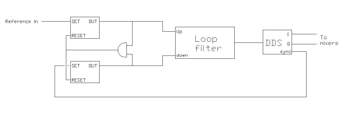
The analog signal was acquired using an A/D converter and fed to a pair of mixers which mix with a pair of quadrature reference signals. The reference signals can be generated by a fixed set frequency onboard direct digital synthesis unit, or derived from an external reference. The external reference signal is also A/D sampled, and then converted to a pulse train which feeds the reference of an add digital phase locked loop(ADPLL). This then generates the output quadrature sine waves. Once mixed down, the signals are fed through programmable digital filters and are then measured and routed by a NIOS II processor. The signal outputs can be directly routed to analog output ports as well as displayed.
For simplicity, both design and conceptual, the low pass filters were implemented via a single pole IIR filter configured to emulate an analog RC filter. This design allowed implementation using minimal system resources as well as minimal complexity, while also allowing easy on-the-fly calculation of filter parameters when changing settings. The parameters could be generated by the NIOS from a user selected time constant. The single pole filter was implemented with two multipliers with filter output given by:
out = a0 * in + b1 * out_previous.
Time constant was selected by tuning a0 and b1 according to:
b1 = e^(-1/d)
a0 = 1 - a0
Where d is the time required to decay to 1/e in number of clock ticks.
In order to allow maximal flexibility of the device, a NIOS II processor was also implemented to control the signal path. Although not explicitly shown in the figure, the NIOS acts as a high level control system, switching signals from the the lockin components to the output. In this fashion, the output DACs can be used to output signals from any part of the signal path including the reference sources, giving the advantage of maximal flexibility as well as a useful tool in debugging. In addition, the NIOS can be used to control filter operation/decay time.
Implementing these components in FPGA allows all operations after A/D sampling to be done digitally at high speed. The target platform for this project was the Altera DE-2 board with a Cyclone II FPGA, speed grade 6, with 35K logic elements. The lockin design should fit easily within this chip and looking up the speed specs for this speed grade gives an advertised 18 x 18 bit multiplication of over 200MHz. This type of clock speed is probably not attainable for the system a whole, but clocking at 50MHz should be entirely stable. As a reasonable expectation, input signal sine waves operating at frequencies of up to one or two MHz should be easily achievable at these clock rates.
User Interface:
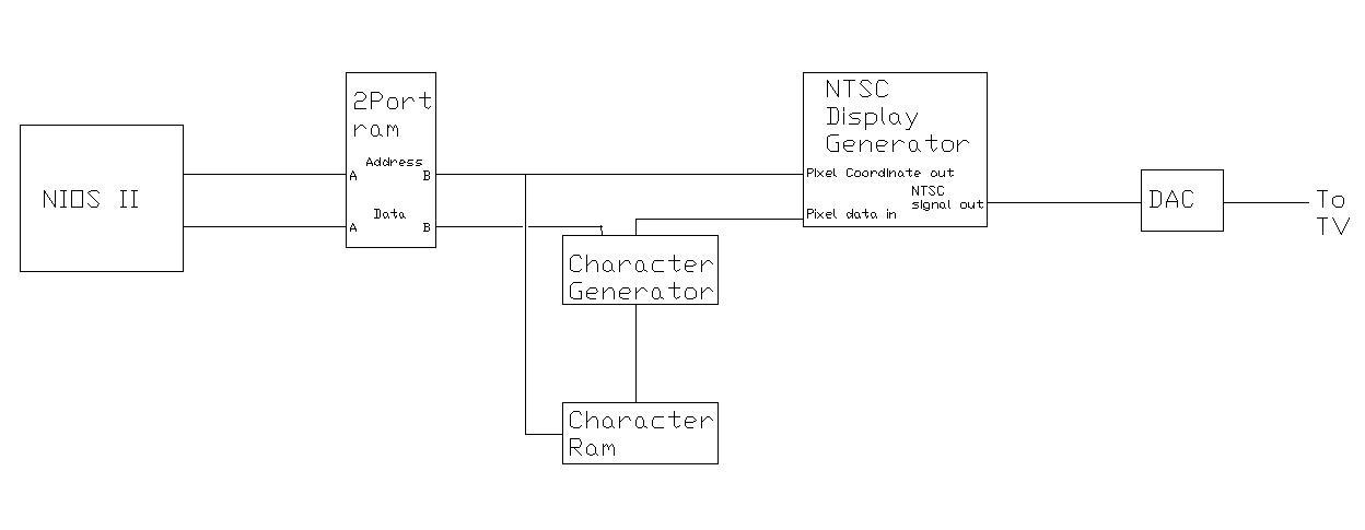
For basic lockin functionality, a number of settings must be entered and displayed by the user. Control of the reference, whether external or an internally set frequency, as well filter bandwidth are essential. In addition control of the output signals along with the ability to display information about current measured values is useful. To this end, it was decided to generate a video display output from a NIOS II processor. The NIOS II processor provided plenty of processing power to generate an output display as well as handle user input and control elements of the lockin signal path.
Hardware implementation
overview:
The entirety of the digital components of this project were implemented on a Terasic DE-2 board with an Altera Cyclone II FPGA. The DE-2 board provided the majority of the hardware components needed, such as the basic FPGA support circuity(power supply, programming, etc), as well switches and buttons for user input along with a VGA output port. The only real lack of this board for a lockin is the absence of a high speed A/D converters. A number of A/D options were considered for the project, mostly based on a homebuilt add-on board, but it was decided in the end to use a Terasic P0003_GPIO high speed digital acquisition daughterboard.
The Terasic product was chosen primarily due to it's convenience, but also had a quite high sampling rate. The board is designed to interface with the DE-2 board and includes two ports of 100MS/s 14 bit DAC outputs and 2 ports of 65MS/s 14 bit A/D input. This was deemed entirely sufficient for a design goal of 1MHZ input bandwidth and gave a good option for either high frequency reference outputs or low frequency output signals.
Unfortunately, as discussed in more detail later, the Terasic board failed to meet expectations. Of critical importance for the intended application, both the input and output ports on the board were coupled via transformers which had an effective cut-off of ~100KHz. For input signals this simply limited the range of measurement to signals above 100KHz -- an annoyance but still functional. In order to output the low frequency or DC measured signals, however, the output ports simply do not work.
To get around this problem, two DAC ports of the VGA output chip on the DE-2 main board were used. The VGA interface featured 3 10-bit DACs rated at up to 100MS/s and allowing DC outputs. While slightly low in resolution, these ports fit the output needs well. Unfortunately, the use of two of the VGA DACs precluded the output of a VGA video, a necessary component of the user interface. To get around this issue, it was decided to use the third VGA output DAC to generate an NTSC signal for display on a standard TV. The resolution of this display is certainly lower, but was acceptable.