SillyScope


The SillyScope is a user-friendly oscilloscope that uses Altera DE1 SoC.


We built the SillyScope, a 4 channel oscilloscope using DE1 SoC. Users can control the oscilloscope using HPS. They can control the voltage scale, time scale, offsets, and the channel to trigger. Users can also perform math operations such as addition and subtraction with two channels. The project uses the HPS to allow user interaction and the FPGA to sample signals and display it on VGA screen.

Find out more!

High-Level Design


The idea for this project came from two of the team members who had a lot of problems with an old oscilloscope. We decided to make our own oscilloscope just to see how good we can make it. The onboard ADC for DE1 only has 500ksps but we believed that was enough to test simple signals. We knew that it was not going to be close to the performance of professional oscilloscopes but it would be good for a final project.

The high-level design overview can be seen in Figure 1. The 4 analog input signals are sent directly to the DE1-SoC’s ADC, an LT2308. The adc module interfaces with this ADC and fetches samples from the active channels at maximum speed. These samples are then sent to the time_scaler module, which discards samples such that a desired effective sample rate is achieved. These samples then flow into the trigger module, which maintains a circular buffer to store the 320 samples prior to a trigger event. These samples are also passed to the triggerer module, which identifies when a trigger event occurs. When a trigger occurs, the trigger module then stores the next 320 samples, to capture a 640 sample window surrounding a trigger event. These 640 samples are then written out to the sample buffer, and upon completion a screen redraw is requested from the vga_writer module. vga_writer then reads the sample buffer and draws the waveforms in the VGA framebuffer. At the same time, the HPS draws a user interface into the overlay framebuffer. The two framebuffers are then merged, and sent out to the screen.

The FPGA was used for sampling the signal, triggering and displaying the signal on VGA display. The HPS was responsible for configuring the FPGA with user specified parameters. We wanted the FPGA to perform almost all the computation for an oscilloscope. We left the user interactions to be handled by the HPS. User interactions are much easier to handle with the HPS and did not add much overhead to computation so it was beneficial to use software for it.

High Level Design

Figure 1: High-level design overview

Hardware Design


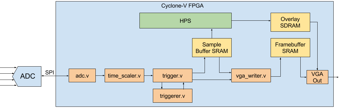
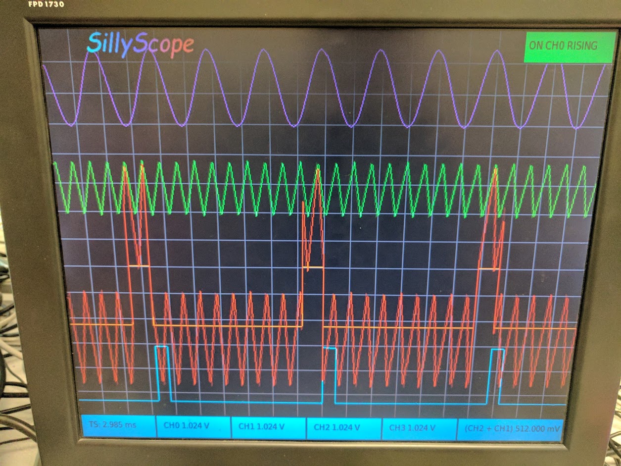
For our design, we chose to push as much of the oscilloscope functionality to the FPGA as possible, with the HPS responsible for configuring the FPGA with the various oscilloscope parameters. All communication from the HPS to the FPGA was done using a simple interface we called the cfg bus. The cfg bus provides a simple write-only method for sending configuration from the HPS to the FPGA. The output of a single HPS-connected 32-bit Peripheral I/O (PIO) module is connected to every configurable module in our design. A number of configuration registers are connected to this bus, each with a register ID. When the upper 8 bits of the cfg bus signals match the register’s ID, the register then stores the lower 24 bits itself. Using this interface, the HPS pushes new settings to the FPGA when the user makes a change to the oscilloscope configuration. Table 1 provides a list of all configuration registers used in the design.

ID Purpose Default Value
1 Timescale Counter Limit 0
3 Math Waveform Enable 0
4 Number of Active Channels (0-Indexed) 0
5 Triggering Mode 0 (Rising)
6 Triggering Enable 0
7 Triggering Level 0x800 (50%)
8 Triggering Pulse Width 0
9 Triggering Source Channel 0 (CH0)
10 CHO Vertical Scale Factor 4
11 CH0 Vertical Offset 0
12 CH1 Vertical Scale Factor 4
13 CH1 Vertical Offset 0
14 CH2 Vertical Scale Factor 4
15 CH2 Vertical Offset 0
16 CH3 Vertical Scale Factor 4
17 CH3 Vertical Offset 0
18 Math Vertical Scale Factor 4
19 Math Vertical Offset 0
20 Math Mode 0 (ADD)
21 Math Source A 0 (CH0)
22 Math Source B 1 (CH1)
30 CH0 Waveform Color 0x3b
31 CH1 Waveform Color 0xec
32 CH2 Waveform Color 0x5c
33 CH3 Waveform Color 0xc7
34 Math Waveform Color 0xe0

Table 1: List of configuration registers used in design

ADC Controller


Initially we used the ADC controller provided by the Altera University Program IP. This was connected to the rest of our design over the Avalon-MM bus through the University Program provided External Bus to Avalon Bridge (EBAB). However, this controller had several shortcomings, the most important being that it’s sample rate was not near the ADC max sample rate of 500 KSPS and it was not configurable during runtime which channels were sampled. Because we needed both of these features, we decided to implement our own controller for the ADC.

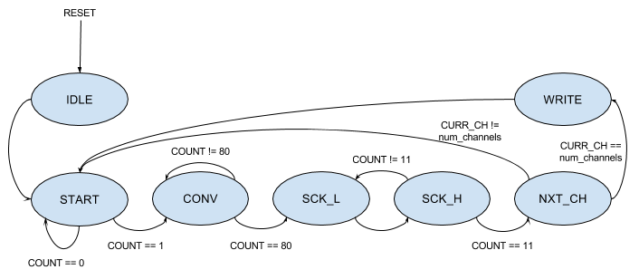
The onboard ADC is the LTC2308, which communicates over the SPI interface. The sequence of operations for a conversion is to pulse the conversion start line high to start the conversion, then the controller must wait for the conversion to occur. After the conversion time, the controller pulses the SCK line for twelve cycles and shifts in the 12 bits of data on the MISO line. The data on the MOSI line for the first 6 cycles of SCK setup the next ADC conversion. Since the maximum clock frequency of this interface is 40 MHz, but the controller is running on a 50 MHz clock, each SCK cycle consists of two cycles of the controller clock. This results in the controller only achieving a sample rate of 471 KSPS. It would be possible to run the control module on a different clock and refactor the module in order to raise this sample rate to the ADC max of 500 KSPS.

The state machine for the ADC controller begins in the IDLE state at reset where all the outputs and states are reset back to their initial conditions. On the next cycle the FSM moves into the START state which is the only state where the CONVST pin on the ADC is high. The FSM uses a counter to remain in this state for two cycles to keep the CONVST pin high for long enough for the ADC to detect it and begin the conversion sequence. The counter then continues to increment while in the CONV state. The FSM stalls here until the counter reaches 80 to give the ADC enough time to complete the conversion.

Once the counter reaches 80, it is reset back to zero and the controller starts the SPI transaction to read in the data. The FSM alternates between the SCK_L and SCK_H states which set the SCK line to either low or high, respectively. The counter is incremented whenever the FSM reaches the SCK_H state and the FSM exits this back and forth loop once the counter reaches 11, indicating 12 cycles of SCK have occurred.

The input data is latched on the rising edge of the SCK line, so on each transition between SCK_L and SCK_H, the value on the MISO line is left shifted into the MISO value register. In order to setup the ADC, the correct bits must be set on the MOSI line. The value of the MOSI signal is updated on the transition from SCK_H to SCK_L to give an entire cycle of setup time before the ADC reads the value.

Once the SPI transaction is complete, the FSM moves to the NXT_CH state, which handles sampling multiple channels. If the current channel being sampled is not equal to the number of channels active, the current channel is incremented and the FSM moves back to the START state to immediately start the next transaction. If the current channel is equal to the number of channels active, indicating all the channels have been sampled, the current channel is reset back to the first channel and the FSM moves into the WRITE state. In the process of updating the current channel, the MISO data for the next SPI transaction is set. Regardless of whether the FSM proceeds to the START or WRITE state, the 12 bits of data that was just read in from MOSI is set to the current channels data buffer.

The WRITE state is responsible for passing the adc data to the rest of the design. If multiple channels are active, all of the channels are updated at the same time. Since there is a max of four channels, this corresponds to a 48 bit value. Because the sampling rate for the ADC should be constant, we do not want to let the FSM stall due to backpressure from later in the design. To accomplish this, the module simply copies the data from the active channel buffers to an output buffer and sets a valid flag in the one cycle it is in the WRITE state. This valid flag remains high until the rdy input is set, indicating that the value was consumed. This design keeps the ADC at a constant sample rate, but if the value is not consumed before the ADC has completed another conversion it is lost.

ADC FSM

Figure 2: FSM for ADC controller module

Time Scaler


We used a simple scheme to adjust the sample rate when the user wanted to view signals that were too slow to be seen at the ADC’s maximum sample rate. Rather than have the ADC controller slow down its sample rate, we instead added a time scaler module which just dropped n samples out of every n+1 samples received from the ADC controller. The value of n was configurable through a configuration register, which allows the HPS to divide the effective sample rate by any integer. This division was accomplished by creating a counter which incremented every time the ADC controller produced a sample, and reset to zero when it reached n. The time scaler then only passed a sample through to the next stage when the counter equaled zero.

Trigger Module


The process of triggering traditionally consists of three steps, which are shown in three of the states of the trigger module FSM: ARMED, READY, and TRIGGERED. In the ARMED state, samples must be collected in order to have data points before the trigger point. Since the trigger point is set in the middle of the screen on our oscilloscope, this corresponds to 320 points. Once the buffer of 320 points has been filled, the FSM moves into the READY state. Here the module is looking for the trigger condition to be met to advance to the TRIGGERED state. The actual trigger detection is handled by the triggerer module. While waiting for the trigger condition, the samples to the left of the trigger point must be kept up to date. To handle this, the buffer from the READY state is treated as a circular buffer with a head and tail pointer that are updated with each new sample. When the trigger condition has been met, the samples to the right must be acquired. Another 320 samples are fed into this new right buffer.

Now that the two buffers are filled, the data is ready to be passed out to the Sample Buffer SRAM where it can be read by the HPS and the VGA Writer. The FLUSH_LEFT and FLUSH_RIGHT states are responsible for writing the values from the left and right buffers into the SRAM over the Avalon-MM Bus. Once all of the 640 samples have been written into the Sample Buffer SRAM, the FSM moves into the SEND_REFRESH state to indicate to the VGA Writer that there is a new data in the buffer. The FSM waits for the ready signal from the VGA Writer to advance back to the ARMED state.

The Trigger module is also responsible for the math channel. Based on the status of the config registers, the samples of any two channels can be added or subtracted to calculate the math channel samples. This operation occurs during the FLUSH states when the points are being written to the Sample Buffer SRAM.

Triggerer Module


The Triggerer Module is capable of detecting triggers based on edges and pulses. The five modes supported are Rising Edge, Falling Edge, Pulse Greater Than, Pulse Less Than, and Pulse Equal to. The HPS can set configuration registers to set which channel is sampled on, as well as the sample level and pulse width. Additionally, triggering can be disabled causing the module to always output a trigger signal.

The first step in the triggering logic is to detect whether the selected input sample is greater than the trigger level. For the edge triggers, the previous value of this signal is stored. The rising edge trigger is then simply that the current sample is greater and the previous sample was not. The falling edge trigger is the reverse. While this trigger logic very simple, it works surprisingly well. Adding a small low pass filter to the sample input prior to comparing to the trigger level would increase reliability on noisy data near the trigger level.

The pulse triggering logic detects the start of a pulse based on the sample greater than trigger level flag. Once the pulse has begun, a counter is incremented each cycle. If the sample greater than trigger level flag goes low, the counter is compared to the pulse length configuration to set the triggers for Pulse Greater Than, Pulse, Less Than, and Pulse Equal To. The counter is then reset and the logic is ready for the next pulse.

Trigger FSM

Figure 3: FSM for trigger.v

VGA Writer Module


The VGA writer was responsible for pulling data from the sample buffer, and writing that display into the VGA framebuffer. The VGA writer received a “go” signal from the trigger module, to indicate that new data was available and the screen should be redrawn. Additionally while drawing the screen, the VGA writer drew a grid in the background. The VGA writer had two main interfaces -- one to access the sample buffer, using an EBAB, and the other directly connected to the framebuffer SRAM. The was also an idle signal, used to prevent the trigger module from modifying the sample buffer in the middle of a screen draw, which would produce visible discontinuities in the output.

VGA FSM

Figure 4: FSM for vga_writer.v

The VGA writer was implemented using a fairly straightforward state machine. The module initialized in the WAIT state, which just waits until the trigger module gives the go signal to start a redraw. After being signalled to start, drawing begins drawing the leftmost column moves into the FETCH state. In the FETCH state, the module reads the values in the currently active column for all 4 channels and the math channel out of the sample buffer. Since this data is tightly packed into a single 64-bit word in the sample buffer, fetching a column’s data is accomplished with a single read operation.

After the sample buffer responds with the data, the FSM moves on to the PROCESS state, which preprocesses the data for display. In the PROCESS state, each channel’s sample value gets scaled and offset by the configuration parameters for that channel, converting the 12-bit sample to a signed 11-bit y-coordinate on the screen. 11 bits are used instead of the 9 required for the 480 rows on the screen because it allows the module to deal with points which are offscreen in a simple manner. Additionally, the y-coordinate of the point in the column directly to the left is saved, to allow drawing a continuous line between the two points.

After the preprocessing cycle, the FSM enters the DRAW state, which iterates through an entire column and writes the color for each pixel to the framebuffer. The FSM remains in the DRAW state until it finishes a column, at which point it goes to FETCH or WAIT, depending on whether or not there are more columns remaining. Pixel color is determined by a set of prioritized rules which are based on the current x- and y-coordinate being drawn. Channels take the highest priority -- if the current y-coordinate is anywhere between the current and previous y-coordinates for the channel, the pixel gets drawn with that channel’s color. This makes the lines drawn on the screen continuous, and deals with edge cases such as square waves well, which generally jump very quickly from their low to high values. The signedness of the y-coordinates also allows this logic to correctly handle all cases where the current sample is off the screen. If no channel should be drawn on the current pixel, then the writer checks if the pixel is on one of the gridlines, and draws the pixel gray if it is. Otherwise, the black background is drawn.

Qsys Setup


For our project, we heavily modified the existing Qsys designs for the main memory system, as well as the VGA controller. The Qsys layout was split into two major clock domains, called sys_clk and logic_clk. sys_clk was a 100 MHz clock used for the HPS’s bus interfaces as well as the VGA subsystem. logic_clk was a 50 MHz clock used for most of our custom logic, and was used as the clock source for the ports of the onchip SRAMs which faced our logic.

Our Qsys design contained a few different memories. There were two on-chip SRAMs which were used to store intermediate data for the oscilloscope. One was an 8 kB SRAM for the sample buffer, which stored samples captured by the trigger module for later display to the screen. The other SRAM was 307 kB, and stored the VGA subsystem. Both of these SRAMs were connected into our logic, and the VGA subsystem also had a connection to pull pixels out from from framebuffer SRAM. There was also an off-chip SDRAM which stored a second framebuffer, referred to as the overlay buffer. The overlay buffer was much larger than the on-chip framebuffer, because it supported full 32-bit color with transparency. This buffer was connected to both the HPS and the VGA subsystem, to allow the HPS to draw over the waveforms.

The HPS’ memory buses were connected into most of the major components, to allow for debugging, configuration, and displaying data. The two main uses of the HPS’ buses interacting with the PIO module driving our configuration bus, and writing pixel data to the off-chip SDRAM. The HPS was also connected to the SRAM for storing the sample buffer, but was not connected at all to the SRAM for the VGA framebuffer.

The VGA subsystem was built to read from two different framebuffers, blend them, and write the blended pixels to the screen. It contained two DMA engines which fetched the pixels from the two buffers and wrote them into a FIFO. Both pixel streams were then resampled into a 10-bit per color channel RGB format, along with a 10-bit alpha term to control transparency of the overlay buffer’s pixels. These two streams were then alpha-blended into the final output color and pushed into a final output FIFO. The final VGA controller then sent the pixels from this FIFO out to the screen over VGA. This design allowed the HPS to create very flexible UI overlays on the screen, without interfering with the oscilloscope operations on the FPGA at all.

While implementing the VGA subsystem, we ran into a problem with the HPS trying to rapidly draw to the screen. In our first implementation, the HPS would temporarily disrupt the VGA output while writing to the SDRAM, though the output would stabilize once the write finished. If the HPS wrote to the entire overlay buffer at once, it would cause a very noticeable disruption in the image on the screen for a moment. To resolve this, we wanted to change the arbitration priorities on the SDRAM controller such that the video DMA would have higher priority than the HPS, effectively preventing the HPS from interfering with a video DMA read. When we tried to modify the priorities, however, we found out that Qsys does not support setting arbitration priorities when the bus is connected to a DMA master. To resolve this, we inserted an Avalon-MM Pipeline Bridge between the video DMA engine and the SDRAM. Qsys allowed us to set the arbitration priority for this bridge, which resolved all of the issues with the HPS disrupting the VGA output. Using this fix, we were able to continuously write to the overlay buffer from the HPS without breaking the VGA output at all.

Software Design


Our HPS program was responsible for configuring the various oscilloscope parameters in the FPGA, allowing the user to reconfigure the oscilloscope over the serial console, and displaying a user interface using the overlay framebuffer. The code was split up into a number of different components which handled those different tasks: the “scope” component maintained and synchronized the oscilloscope configuration with the FPGA, and reported the current configuration. The “shell” component handled the serial console, and passed configuration changes on to the scope component. The “surface” component was responsible for transferring pixels into the overlay buffer, and the “display” component was responsible for rendering the user interface itself.

The scope component had a large number of functions for changing the configurable oscilloscope parameters, storing the current configuration, and reporting the current configuration. At startup, the oscilloscope configuration gets reset to a known state. Whenever a configuration change is requested, the change is passed on to the FPGA configuration bus, and the new state is stored for the display component to read later.

The shell component provided a simple command based interface for updating the oscilloscope configuration. Each command took some number of arguments, for example to specify the channel to modify and the new vertical scale in the “vscale” command. Each command handler took care of parsing and validating the values passed in, and then called into the scope component to update the configuration. Table 2 summarizes the commands which the shell made available.

Command Description
num_chan [n] Sets the number of active channels
timescale [n] Sets the horizontal timescale
vscale [ch] [n] Sets the vertical scale for a channel
offset [ch] [n] Sets the vertical offset for a channel
trig_off Disables triggering
trig_on Enables triggering
trig_mode [n] Sets the triggering mode
trig_chan [n] Sets the triggering channel
trig_level [n] Sets the triggering threshold level
trig_width [n] Sets the pulse triggering pulse width
math_off Disables the math waveform
math_on Enables the math waveform
math_scale [n] Sets the math waveform vertical scale
math_offset [n] Sets the math waveform vertical offset
math_mode [n] Sets the math function
math_ch0 [n] Sets the first source channel for the math waveform
math_ch1 [n] Sets the second source channel for the math waveform

Table 2: Commands available in shell

The surface component handled creating the rendering context used by the display component, and transferred pixels into the overlay buffer. We used the cairo graphics library to handle all rendering on the HPS. Cairo was used because it is a very well-optimized 2D rendering library, and its ARGB32 image surface type happens to store pixels in memory in the exact format used by the overlay framebuffer. Thus, the surface component simply initialized cairo, and used memcpy to transfer pixels from the image surface to the overlay framebuffer when refreshing the user interface.

The display component did all of the user interface rendering using cairo. The cairo context created by the surface component was drawn to for every UI element on the screen. We organized the UI into a series of hierarchical “panels”, where each panel had a background color, edge color, some number of child panels, and optionally a custom drawing function. For most of our UI components, the drawing function simply fetched some state from the scope component, and then drew some text in the panel using cairo. For most panels this was a fairly simple usage of cairo, though the “SillyScope” banner text took advantage of some of cairo’s more advanced features, using masks and color gradients to produce a moving rainbow effect.

Results


We successfully completed the project by having a 4 channel oscilloscope with a good UI. Figure 5 below shows a picture of the screen when all four channels are used. Each channel has a different color which makes it easy to differentiate. The top right hand corner displays the channel and trigger status. The bottom of the screen displays the time/div and volts/div for each channel. If math mode is enabled, the bottom right hand corner will display the math mode along with the associated channels.

We prioritized a clean and colorful user interface which allowed users to control parameters with ease. Thus we created a C program to be run on the HPS side where users can type in commands to adjust parameters. The demo video can be seen on youtube.

In the end we had a very responsive oscilloscope. The screen did not flicker at all and it was able to trigger properly on the specified channel. The HPS overlay of channel information on the screen was essential for a good user interface. The configuration commands from HPS were also performed quickly so the screen was able to update without delay. New users should be able to quickly use the SillyScope because of the clean and understandable UI. The commands are also straight-forward to understand and short which helps users to quickly configure the parameters.

The project did not pose any safety threats to the team members. We had to make sure the FPGA was safe against high voltages especially on the ADC pins. We systematically chose wire colors to make it easier to debug the connections and ensure that nothing was shorted. We did not have any interference with other team’s designs. However, it was interesting to see the capacitive coupling on the channels when one of the channels were not connected but it was still displayed on the screen.

VGA FSM

Figure 5: SillyScope when all four channels are used. It displays the triggering channel in top right corner. The time/div and volts/div for each channel is displayed in the bottom of the screen.

Conclusion


The project met our expectations in terms of final functionality and UI. We were able to support multiple channels and had an appealing design. The commands were intuitive so it is easy for new users to use while also allowing them to configure a lot of parameters. We had originally thought of including a logic analyzer but it was more interesting for us to build a more user friendly environment. In the future, we could look into scaling the number of supported channels to eight which is the maximum number of pins connected to ADC.

We started the project with Altera University Program for complete computer system which included major components like video out and audio. However we changed the program dramatically by deleting all the components that we did not need. This allowed us to have cleaner code and to make debugging easier.

Appendix


The group approves this report for inclusion on the course website. The group approves the video for inclusion on the course youtube channel.

Code as zip file

ADC Documentation

Cairo

DE1 SoC Documentation

SillyScope: A Cornell University ECE 5760 Final Project, Spring 2017