FPGA Convolution Neural Network Accelerator
Project by Yue Ren(yr233), Peidong Qi(pq32)
May 15th 2018
Introduction
Artificial intelligence starts to show its greater and greater potential at serving people’s life, however, its massive computation requirement makes it hard to be implemented within less strong computational tools. Compared to CPU, FPGA is much faster due to its parallel mechanism; Compared to GPU, FPGA consumes way less energy. In this project, we want to use FPGA as an accelerator at calculating CNN structures and in particularly, we will use VGG16 model.
In our design, FPGA is used only to solve convolution computation, and HPS will be used to handle the command and the rest part of layer computation including RELU and max pooling. Due to the limitation of the memory on board, we load input and filters to registers on FPGA line by line in a splitted manner. FPGA behaves like a huge state machine following the command and taking data from and to HPS, and in the meanwhile, HPS will be responsible of handling the data to and from FPGA.
The result we achieve is a 12% acceleration without losing much fidelity when using 16 bit fixed point data format instead of 32 floating point format to reduce the computation workload.
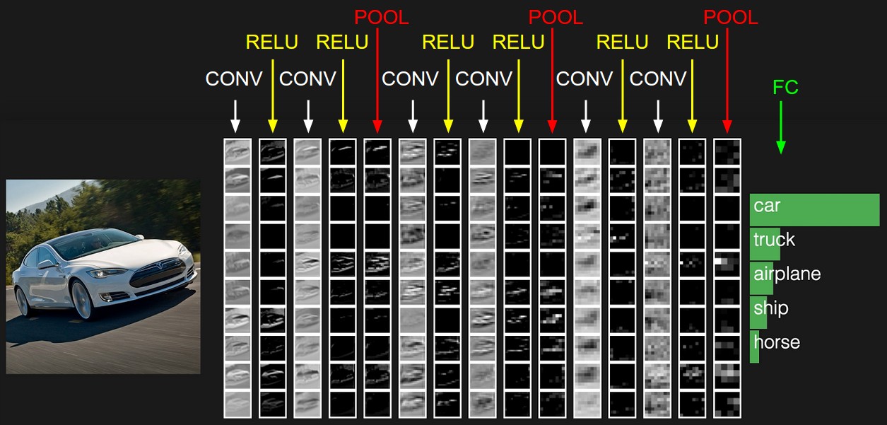
convolution neural network(from [3] Author:Andrej karpathy)
High level design
At high level design, we will use HPS to import an image and decode it. We also use HPS to load VGG16 weights. Then we input those to FPGA. The FPGA will take the calculation part. After calculation, FPGA will output the result to HPS. The result will be the features of the image. The HPS will display the feature to monitor through VGA. For the image input, we pre-processed it using MATLAB. RGB values are extracted and then their mean values are calculated and subtracted from the original data. Subtracting the dataset mean serves to "center" the data and therefore have a better learning speed. In this project, we adopt 16 fixed point format of 1:7:8. In this format, the precision can reach to 0.00390625 and the range from -127 to 127 of the integer part. The input data are between -127 to 127 and all weights are relatively small (typically 0.03-0.3). The conversion of the inputs and the pre-trained weights are done by sfi function in MATLAB. HPS is the main control of the FPGA. It will send command and data for the FPGA to implement and receive the result from the result buffer in FPGA. To implement the pre-trained VGG16 model, we need to load three registers representing three lines of the input in the FPGA through command load_mem. Then we load the first 16 filters to the filter register in FPGA through command load_fil. With the input ready, convolutional computation will perform for the first three lines of the input file and first 16 filters through command compute. Then we read the result from those 16 filters through command getresult and save them in the local files. Next 16 filters will be loaded and we repeat the process until all the filters are processed. Finally, we load a new line and repeat everything again and again until all lines in the input files have been multiplied by all the filters.
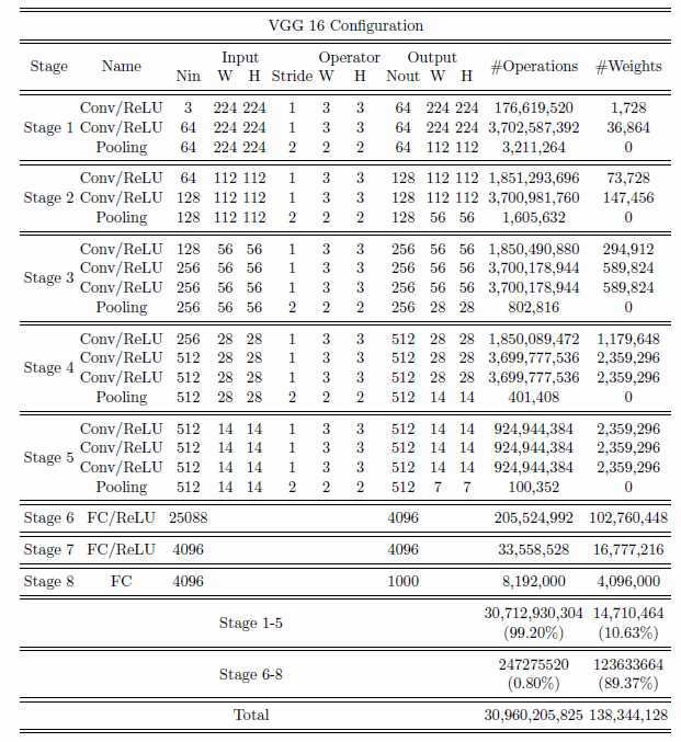
Complexity of VGG 16 neural network(from [5] Author:Huyuan Li)
Convolution Computation
The convolution layer is the most important part in CNNs, which takes more than 90% computation compared of the whole network. The convolution computation formula is shown below:
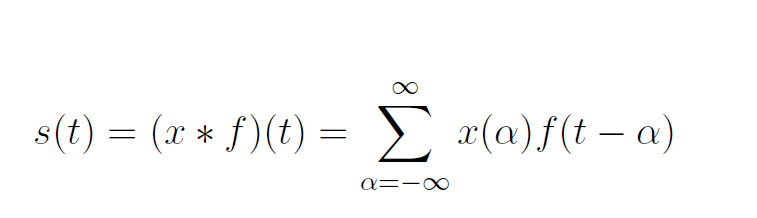
The x(t) and f(α) are referred as the input and weight function. The output is referred as the feature map. For our project, we have used 2D space, the filter is also 2D. Our convolution layer starts with three inputs and one output. The three inputs represent RGB values. Each input represents one channel and each channel is correlated with filters. Then bias is a unique scalar value that is added to the output of convolutional layer at every single pixel. We got all the weights and biases from VGG16 pre-trained dataset. Each input is multiplied with a corresponding filters and the summation makes the output result. The figure below can better explain the working principle of convolution computation.
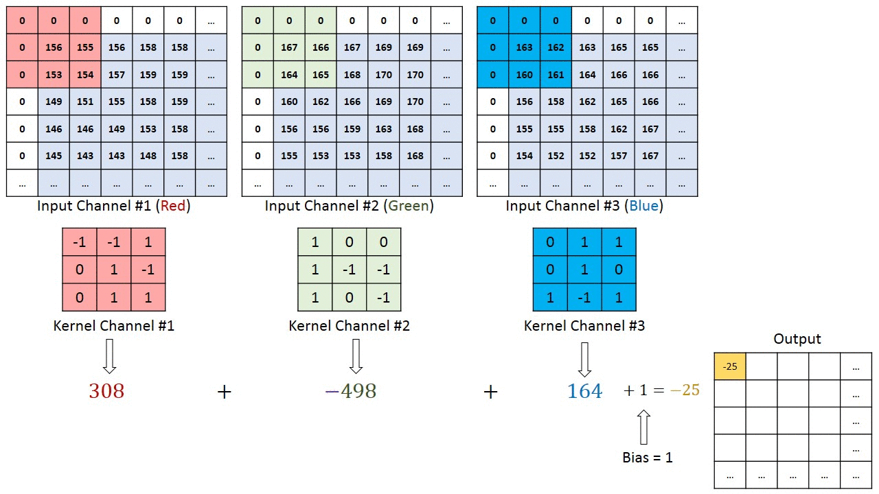
Convolution layer computation(from [4]Author:Hadi Kazemi)
Pooling Layer Computation
The function of pooling layer is to condense the convolved feature maps. The pooling operator has included max-pooling and average-pooling. For our project, we have used max-pooling. We used a diagram to show how to max-pooling works, which slides a window, like a normal convolution, and get the biggest value on the window as the output.
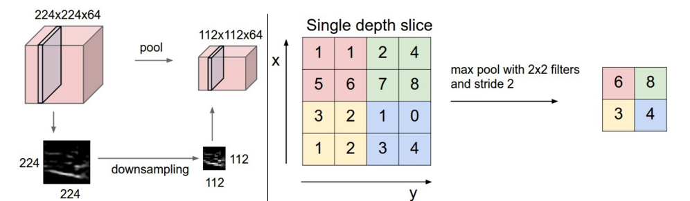
Max pooling(from [3] Author:Andrej karpathy)
Software Design
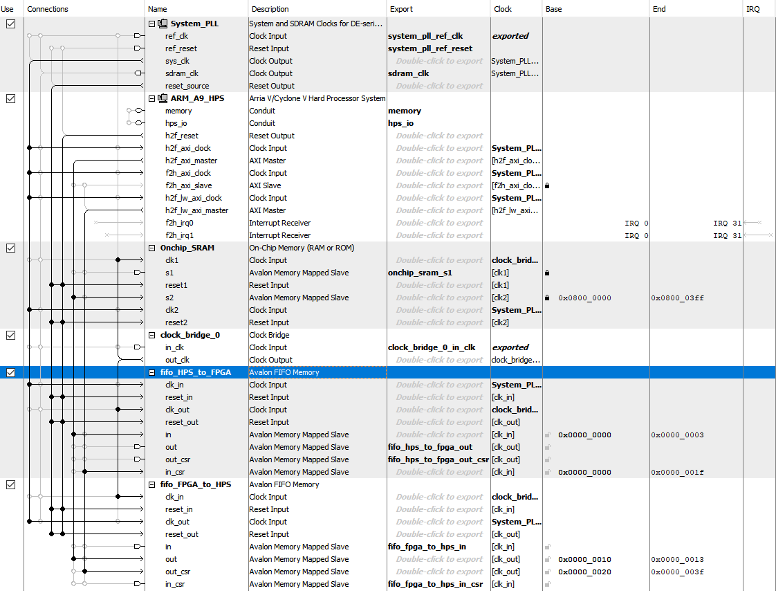
Top-Level Qsys Layout
Verilog Design
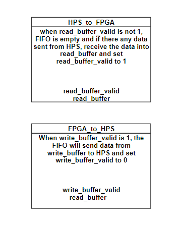
FIFO
For the FIFO design, we are using Bruce’s resource from hackaday as the bridge of communication between HPS and FPGA. In Qsys, two dual-port FIFOs were defined, and each of them has one port attached to the HPS bus and the other exported to the FPGA fabric. The depth of the FIFO we are using is 256 and the data width is configured to be 32 bits. Since the data we use for computation are 32 bits, each time 2 data will be sent. For HPS_to_FPGA FIFO, whenever there is data in, read_buffer_valid will be set to 1 and data will be saved in read_buffer. New data will not be read until we process the data in other steps and set the read_buffer_valid to 0. Similar for FPGA_to_HPS, when we save the data into write_buffer and set the write_valid to 1, FIFO will read that data, and send it back to HPS and set write_valid to 0 for the next input.
FIFO
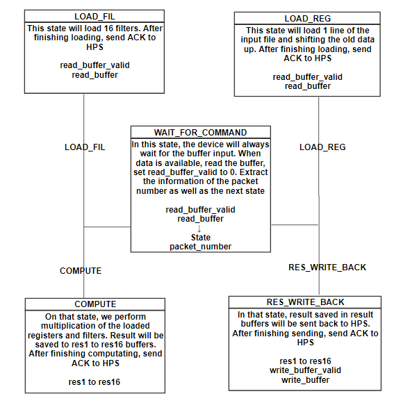
FPGA state machine
WAIT_FOR_COMMAND
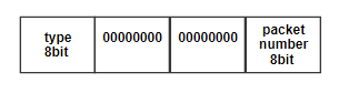
In the WAIT_FOR_COMMAND state, the board will wait for a input from the HPS. HPS will generate a 32-bit command, with the first 8 bit representing the packet number that FPGA is supposed to receive and the type for the next state to go. Upon extracting those information, FPGA will switch to the new state from next clock.
LOAD_REG
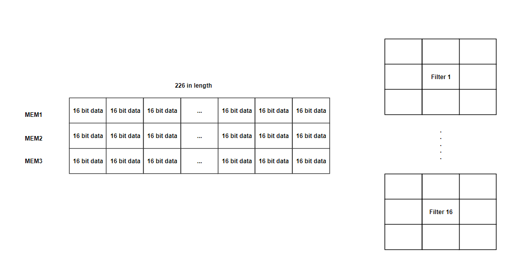
In that state, we have three registers(MEM1, MEM2, MEM3) capable of holding 226 16-bit data. We are using 226 length register mainly for the first stage, which has a 226x226 input size(extra 2 bits for padding), and most of the register will not be used for the following stages. M10K and MLAB is not used here because we want to access multiple data at once. Since the number of registers is quite limited, we split the large input file into lines. In that state, each clock we will load 2 input data to MEM3 and move the old data upwards. After finish loading MEM3(old data shifted to MEM2 and MEM1), send ACK (0xffff) signal to HPS by changing write_buffer_valid to 1 and save the result to write_buffer. Since the filter size is 3x3, we need to load three lines to enable the calculation. Each time we finish the computation with the corresponding filter, we load a new line and restart the calculation with filters.
LOAD_FIL
In that state, we will load 16 filters with the weights we read from HPS_to_FPGA’s read_buffer and those 16 filters will then be used to multiply with the loaded register from left to right in the COMPUTE state. Number 16 is well chosen for two reasons: 1. Each filter will perform 9 multiplication at the same time and therefore 16 makes it 144 multipliers to be used at one clock. As there are 174 multipliers with in DE1-SOC, we ensure the number will not exceed; 2. The number of filters are the multiple number of 16, like 64,128,256,512. If we make it more than 16 or less, we waste cycles to perform such a heavy computation. After loading 16 filters, ACK signal will be sent back to HPS and switch back to WAIT_FOR_COMMAND state.
COMPUTE
We perform multiplication of the loaded registers and filters on that state. Module compute is used to perform the calculation of the register and filter and sum up all 9 results. Genvar is used to generate 16 compute modules outside the always loop. Each module has 1 filter window and 1 register window input. On each clock, COMPUTE state in always loop will raise notein signal to notify the compute module, fill the register window(3x3) and filter windows(3x3). Upon receive the notein signal, compute module will start the computation with the input module and passes notein signal to fixedmul module, where the multiplication of filter and the register windows is performed. It takes one clock to generate the result from fixedmul and pass the value of notein back to compute module as noteout. When noteout is 1, compute module sum up the result from fixedmul and pass the result and noteout to the outside. Notein signal is passed from outside to compute, to fixedmul, to compute and to the outside. The reason why we do so is to synchronize the result and saved it correctly in the result buffer. On every rising edge of the clock, register window will shift right by one and the result capture will have 2 clocks in delay. When we saved all the data in result buffer, ACK signal will be sent back to HPS and switch back to WAIT_FOR_COMMAND state.
RES_WRITE_BACK
In COMPUTE state, results of multiplication of 16 filters on three lines of input from left to right were save in res buffer. At RES_WRITE_BACK state, data from res buffer will be send back to HPS through FIFO. When write_buffer_valid is set to 0 by FIFO, we save two data into write_buffer and set write_buffer_valid to 1, indicating the data is ready. After sending all the result, ACK signal will be sent back to HPS and switch back to WAIT_FOR_COMMAND state.
HPS Design
1.Send_command
This function will generate command for FPGA to set the next state as well as the number of packet it supposed to receive. Data will be send in the format as follow:
2. Load_mem
This function will take a input file pointer, number it needs to read and options of padding. This function will send a line from the input file to the FPGA, each time 2 data in a packet. When padding is enabled, 0 data will be added at the front and end of the line and if that line is the first or the last, a whole line will be sent. After finishing sending out all the data, wait for ACK signal and return with the pointer for the read of next line.
3. Load_filter
This function will take a input file pointer, and send the content of 16 filters to the FPGA, with each filter containing 9 weights. After finishing sending out all the weights, wait for ACK signal and return with the pointer for the read of next filter.
4. Compute
Send out compute command to FPGA and wait for the ACK signal when it finishes the computation
5. Getresult
Send command to FPGA asking for the data saved in result buffer. It will receive the result of one line of the output file for all the filters. Calling it after loading_mem, load_filter and compute.
6. Output data process
For each convolution layer, we will have multiple output text files. For each file, all the datas have been stored in matrix format. Each data is 16 bit hex number in 8.8 fixed point format. We need to convert each hex number to decimal number. And output the new data to a file in future use. Once we get those output files, we can import those files into matlab to generate the image of features.
Testing and Results
We compare the run time and result with and without FPGA accelerator. For the unaccelerated case, we wrote the code purely in C. Data is processed as floating point for result comparison and fixed point for speed comparison.
Result comparison
Since floating point has the highest accuracy, we consider it as the reference and compare how far away our result is from the original one. As we can see from the output result, features we extracted from the first layer of CNN resembles the floating point version. When we explored the data generated from floating point code, we found that a small number of data has value bigger than 300, which exceeds the range of our 16 bit fixed-point format and it shows that, in the FPGA calculation, overflow did happen but the result is not too much influenced. Thus, We can conclude that, although 16 bit fixed-point lose a certain degree of precision and overflow occasionally, the result is still reliable.

Example image
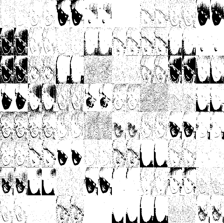
Floating point computation Result
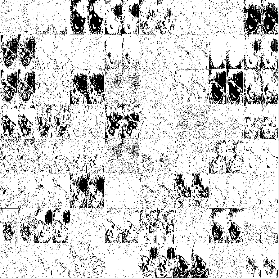
FPGA computation Result
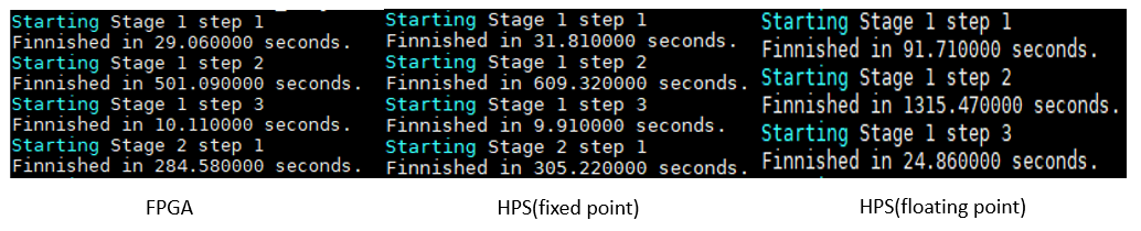
Runtime comparison
Speed_FPGA>Speed_HPS_Fixed_point>>Speed_HPS_Floating_point
It is straight forward that floating point code takes the longest time to run due to its high precision. Our FPGA accelerator is approximately 12% faster at HPS fixed point calculation. Stage 1 step 3 contains only HPS computation and thus has quite a similar result. And FPGA accelerator behaves much better at solving stages that involves heavy convolutional computation like stage 1 step 2. The more the convolutional computation, the better the result.
final Result
Summary
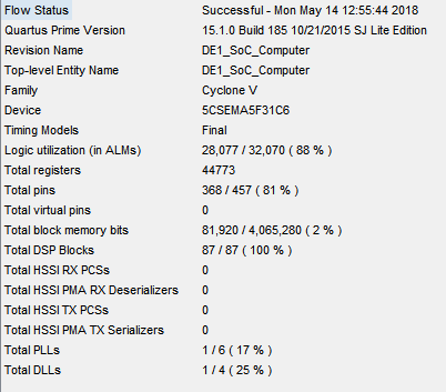
As we can see from the flow state, we utilize all the DSP module and 88% of ALMs. As a matter of fact, during that project, we failed so many times due to the failure at logic utilization. It is through the optimizing the structure that we make it work while not compromising the efficiency. There are three hardest parts that we overcome:
1. Saving data into registers and read them out:
It may looks easy but during the development of code, we always failed to receive the data from FIFO and save it to the register. At that time it is not straightforward where the problem lied, and all we can do is to blink the LED to guess what was really happening within the board. After breaking big thing into smaller pieces and simulated it in ModelSim, we made it work.
2. Compute module to perform the calculation
a. Debugging compute module
i. To find this synchronized method takes a certain amount of effort. Because we cannot call a module like a function within always loop, we have to find a way to synchronize the input to the outside-always module and know exactly when the result is ready for read.
ii. Misuse of wire and reg. Verilog does not generate error message for the connection, but in reality, data always failed to be passed out from fixedmul and compute module.
b. Choosing between floating point and fixed point.
Our initial design used 16 bit floating point , but later we found it takes too much space and resource. To add 9 results up takes 4 clocks in FPGA, and to make computation on the HPS side, we need to design extra functions handling multiplication and addition, which is highly complicated and slow. Hence we abandon that format and use fixed point format instead.
3. Long time compilation
As the project grows bigger, it takes longer and longer time to debug. Usual compilation time is 20 mins to debug for a small thing.
FPGA Result
Conclusions
Our system is designed for convolutional computation. It is not only limited to VGG16 and can also be used to perform computation for all CNN structurals. The main goal of this project is to testify our idea that FPGA can be used to solve convolutional computation, and can accelerate the whole process.
The result shows that our FPGA did slightly accelerate the process. Although the acceleration is not significant, there is still much space we can improve on. In this design, we didn’t change the original design of the FIFO, and we kept it with word width of 32 bits.The maximum word width is 256 bits, meaning we can send 16 data at the same time instead of 2. Also, the clock we are using is the slowest one to ensure not to mess up with the rest of the system. CLOCK_50 is only 1/16 of the fastest clock and is way slower than the communication between HPS and FPGA and other calculations. So to better improve the efficiency, we will first increase the word width of both FIFOs to 256 bits, which will be 8 times faster than our current design. Then, we will use a faster clock. Considering FIFO state machine takes two clock cycles to complete a read or write and the existence of bus latency, our design has an potential approximately 64 times faster!
The bottleneck of the FPGA CNN solver is at the limitation of memory. As there is no way to save all the data on the board, we have to move data between HPS and FPGA and most of the time is lost here. DE1-SOC board is the a good choice to perform FPGA calculation, and we tried to make the best out of it. As a matter of fact, currently there is no good structure of FPGA dedicated for CNN acceleration. This project gave us a good insight of what a future FPGA CNN accelerator would be like, and possible ways of handling with data.
Intellectual Property Considerations
For all the verilog code and HPS code, all the work belong to our own.
Legal Considerations
There is no legal consideration in our project. We used usb cable to transfer our data instead of wireless transmitter. We have not use any device may harm to human. And we did not infringe any Intellectual Property.
Appendix
Appendix A
The group approves this report for inclusion on the course website
The group approves the video for inclusion on the course youtube channel
Appendix B: code
Appendix C: Work Distribution
Yue Ren
Helped write and debug all Verilog code. Wrote and debugged all HPS code. Wrote hardware, HPS (software), and results sections of this website. Created, designed, and formatted this website.
Peidong Qi
Helped write and debug all Verilog code. Wrote and debugged all HPS code. Wrote hardware, HPS (software), and results sections of this website. Created, designed, and formatted this website.
Appendix D: References
Great thanks to Prof Bruce Land for his guidance. Every time we hit a roadblock or got to the wrong way, Prof Land always guided us to the right path. We would like to thank all TAs from ECE 5760. They helped us a lot.
[1]Acceleration of Deep Learning on FPGA
[2]FIFO interface between arm and fpga on de1-soc
[3]CS231n Convolutional Neural Networks for Visual Recognition
[4]Undrestanding Convolutional Layers in Convolutional Neural Networks (CNNs)
[5]Li, H. (2017). Acceleration of deep learning on FPGA (Order No. 10257690). Available from ProQuest Dissertations & Theses Global. (1886839441). Retrieved from https://search.proquest.com/docview/1886839441?accountid=10267
All the pictures' copyright are belong to original author