Lattice Boltzmann Fishing Game
A Project By Siddhant Ahlawat and Qingyuan Xie.
Demonstration Video
Introduction
In this project we have built a fluid simulation-based fishing videogame and implemented it using two different hardware acceleration approaches on the Dec1-Soc development board. The fluid is modeled using the lattice Boltzmann algorithm as it provides a good approximation of fluid physics and can be easily parallelized on an FPGA. The Challenge of this project was to create a hardware accelerator for the fluid simulation to make it more real time and appropriate for the gameplay. The acceleration reached by the two accelerators were x1.2 and x53 respectively with the limiting resource being memory.
Project Objective:
- To create a real-time and fun video game using the lattice Boltzmann algorithm.
- To achieve maximum hardware acceleration using the Dec1-Soc development board.
Mathematical Background
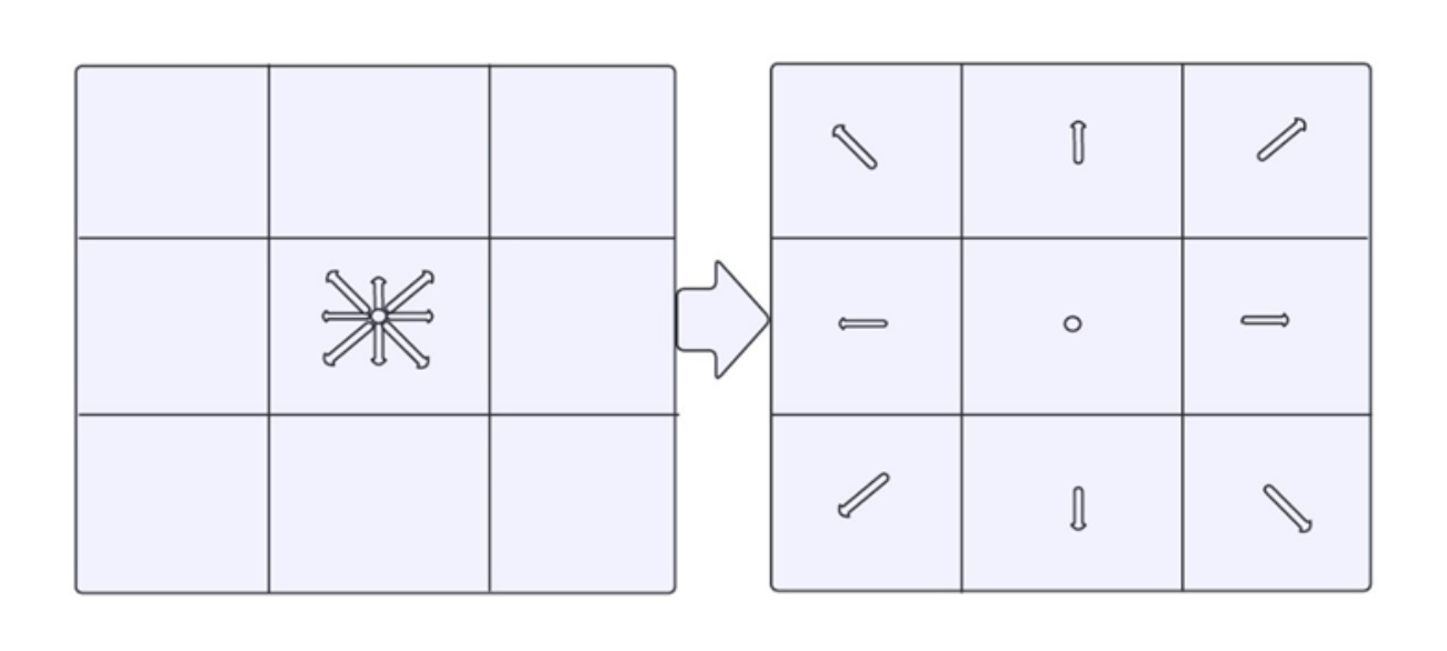
The lattice Boltzmann algorithm was developed as an alternative to conventional CFD approaches that usually work by solving the Navier-Stokes equation to simulate fluid physics as there was a pressing need to accelerate the simulation to reduce simulation times. In this algorithm the fluid is imagined to be made up of a lattice (grid) of imaginary particles that perform two operations- streaming and collision. These imaginary particles are associated with 9 densities which quantify the tendency of the density of that particle to be in one of the 9 possible states in the future, each state being a possible direction of motion, i.e. North, South, East, West, North-West, North-East, South-West, South-East and Null(stationary particle).
During the stream process, these densities are propagated in the lattice in the direction associated with them, i.e., the East density of a particle is copied to the East density of the particle to the right of it, the West density copied to West density of the particle to the left of it and so on as shown in the figure below.
This behavior is mathematically described below:
During the Collision process, the 9 new densities obtained after streaming are adjusted in each particle to conserve mass and momentum. This behavior is mathematically described below:
Design
Fixed point usage
The values of amplitudes are converted to 2.25 fixed point format in this project, as it achieves the desired level of precision and minimizes the number of DSPs required.
As the limiting resource was identified to be memory, it was kept in mind while deciding precision required.
The conversion required a fixed point multiplier to be built in the Verilog which basically performs a full multiplication and truncation to realize the fixed point multiply.
Use of Arm+fpga
For Accelerator 1
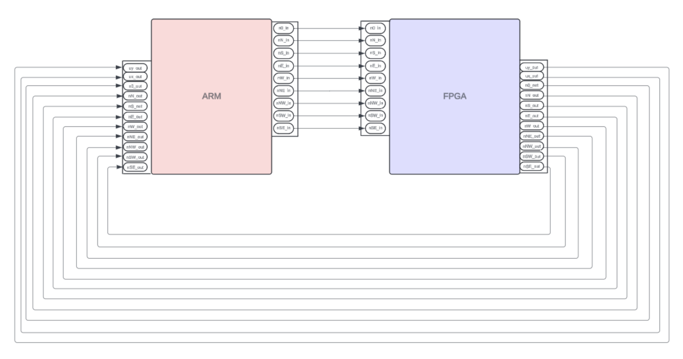
The interconnection between the ARM and the FPGA of accelerator 1
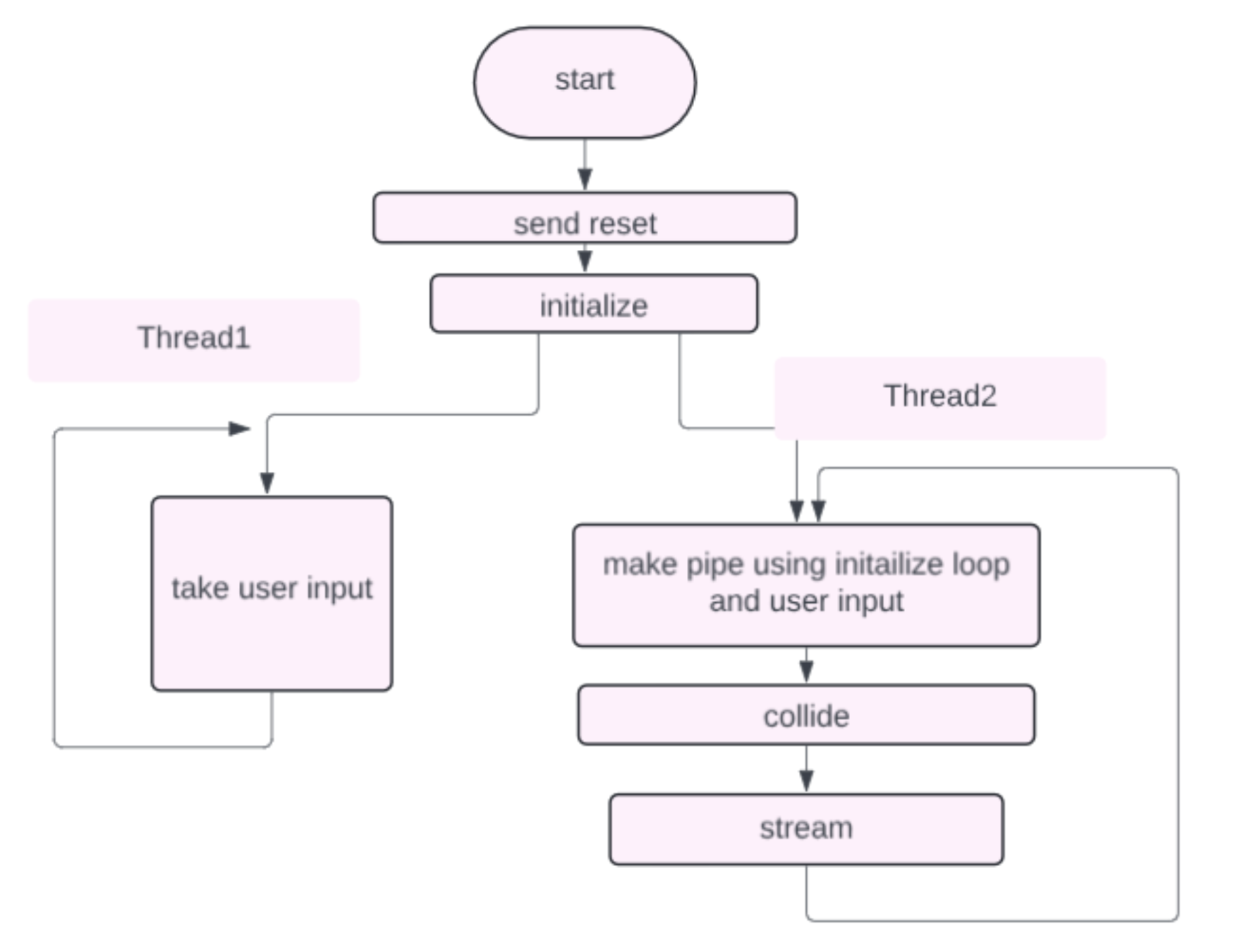
1. ARM - The ARM runs the entire videogame and just offloads the collision computation on the FPGA. The data in this approach is stored in the off-chip SDRAM and accessed serially by the ARM.
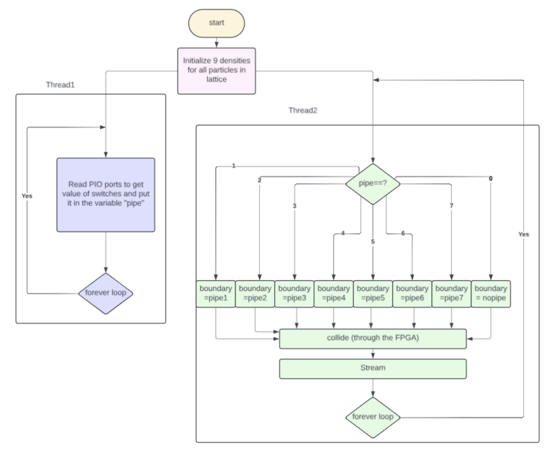
Flow diagram of ARM for accelerator 1
The Game logic goes as follows-
We start by initializing the lattice with all particles getting their 9 densities. All data is stored in 1D arrays on the SDRAM.
We then create a pipe by giving the boundary walls of the lattice - speed in some direction (direction of water flow we want) by adjusting the 9 densities accordingly.
We then enter two forever loops running on two different threads, one that takes in the user input by reading the switches on board, the other running the streaming, collision and boundary write functions.
When the user input changes, different boundary values are written for the lattice in the other thread.
The streaming is performed completely on the ARM, while in the collision function, we send the old densities to the FPGA and get the new densities and the calculated speeds of particles back to the ARM.
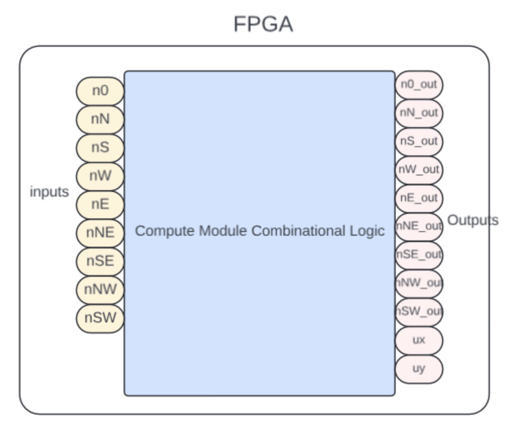
2. FPGA - The FPGA computes the mathematical equation of the collision operation when prompted by the ARM and sends it back. It receives 9 densities of a particular particle and sends back the computed new 9 densities and two speeds- vertical and horizontal (y,x) to the ARM.
Design Tradeoffs
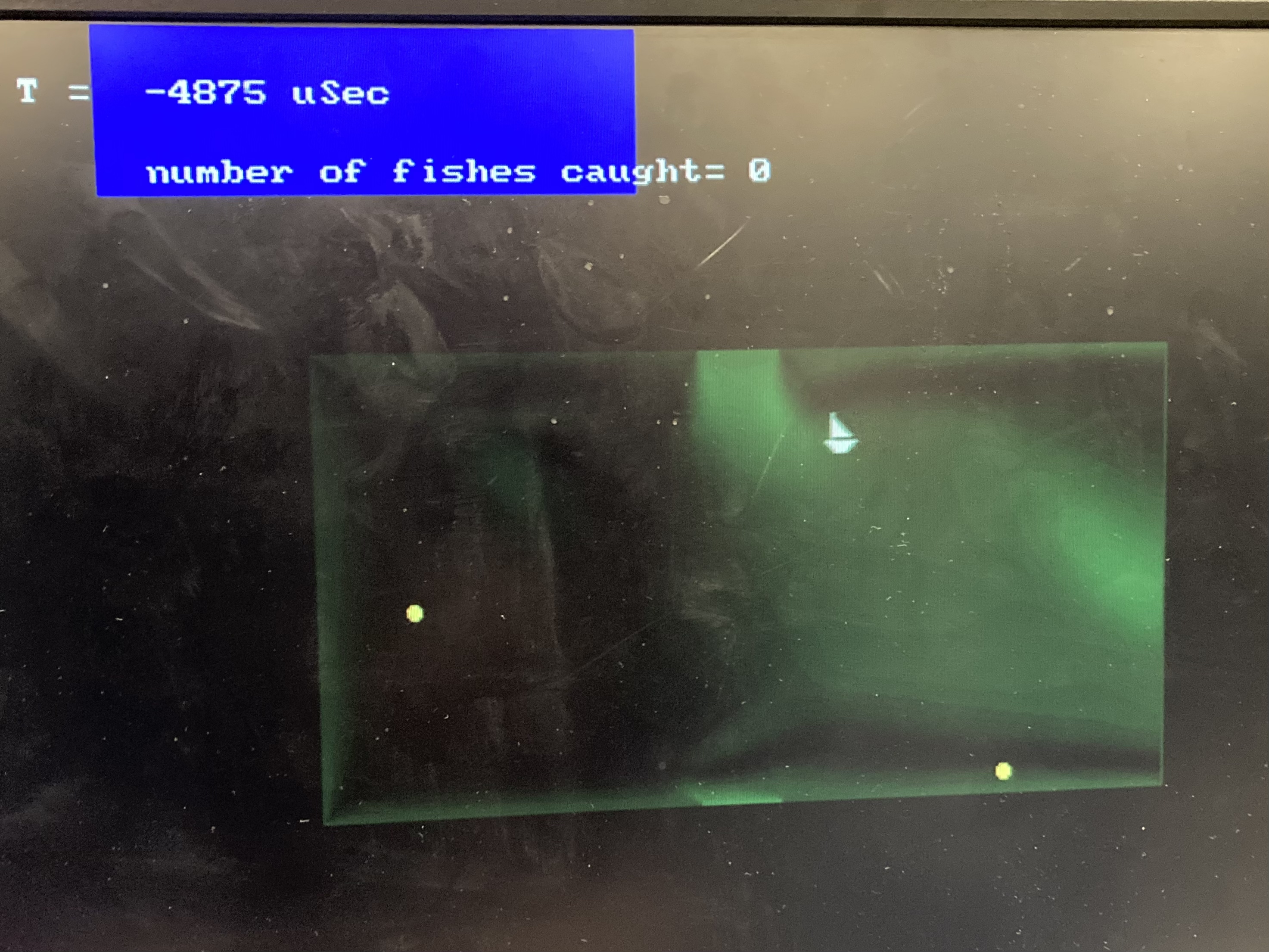
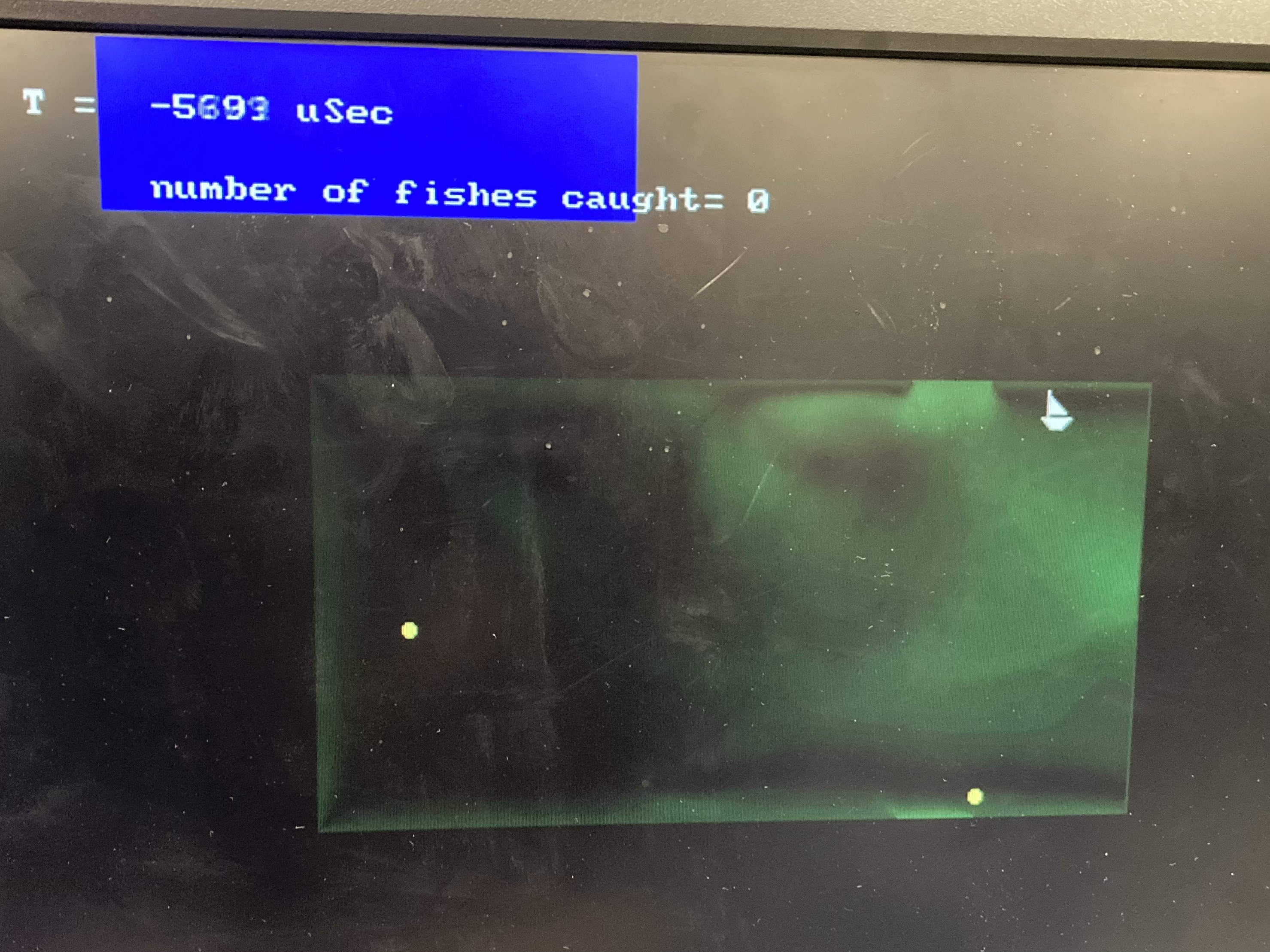
Since the SDRAM has 64kB of capacity which is greater than on-chip memory for FPGA, we can have a bigger lattice in this approach and therefore a bigger playable area in the videogame.
The serial memory access with a bigger lattice makes the game considerably slower than the other approach.
The code is much simpler to write and change, reducing development time and effort.
The communication time between the ARM and the FPGA (AXI lightweight bus and Avalon bus) also eats away some acceleration time.
For Accelerator 2
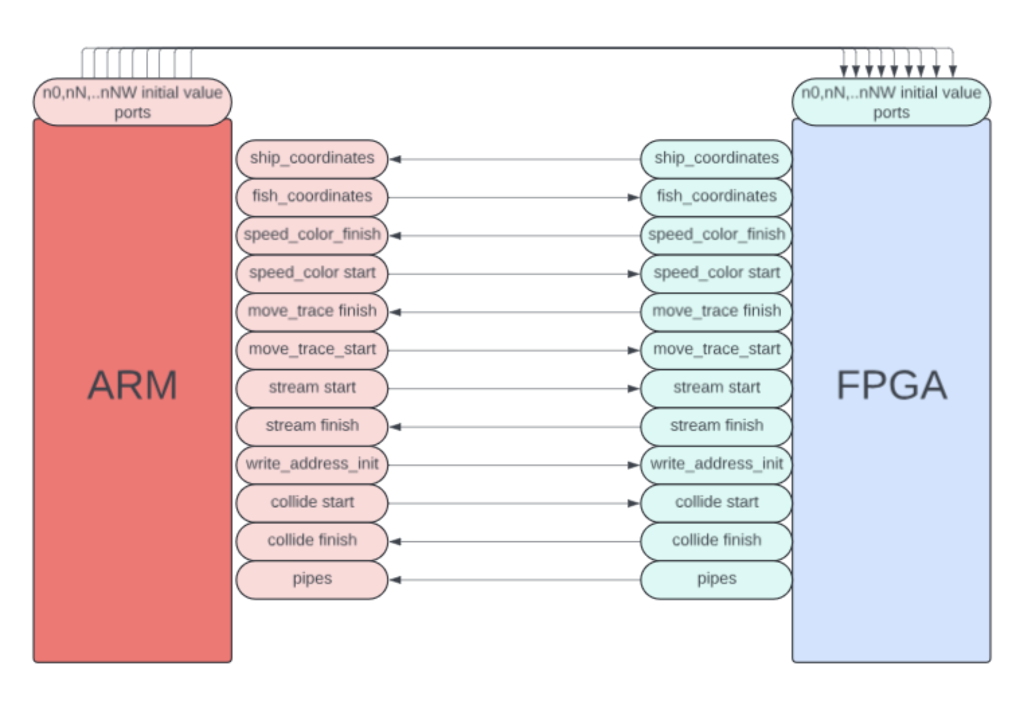
The interconnection between the ARM and the FPGA of accelerator 2
There are 5 main operations that are performed on the FPGA using finite state machines- Initialize, collide, stream, move ship, color_vga. The scheduling of these operations relative to each other is controlled by the ARM through some control signals that carry out a handshake mechanism between the two different clock domains. The densities are stored in M10K blocks accessible to the FPGA for fast memory access.
1. ARM - The ARM does the scheduling of operations and initializing of the memory
Flow diagram of ARM for accelerator 2
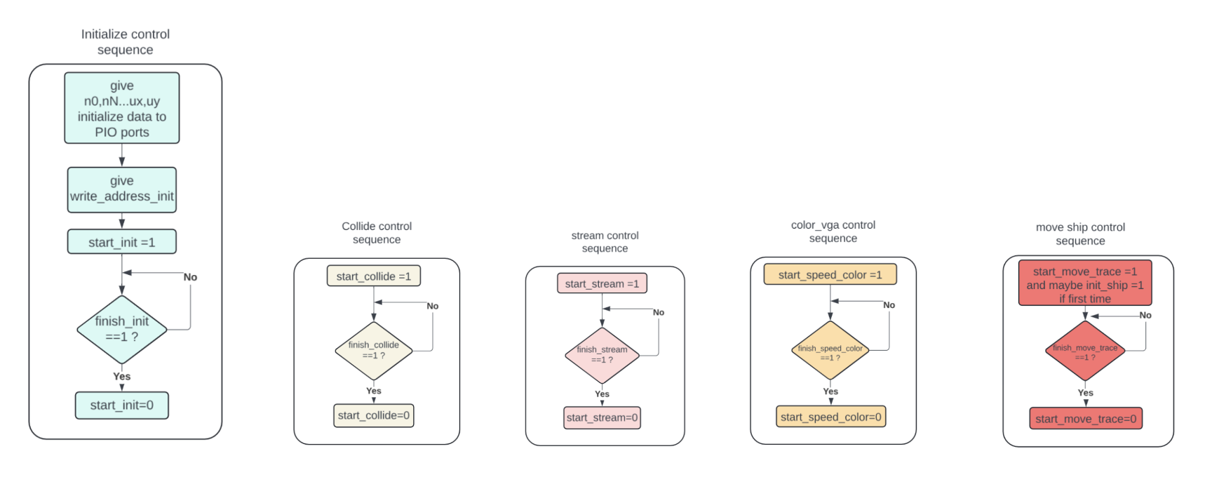
First the FPGA FSM’s are reset using a signal sent by the HPS through the PIO ports.
Then the M10K blocks containing the densities, speeds, color data are initialized. To write to a particular address in all M10K’s, the HPS first sends the values of densities, speeds and color value to be stored in those addresses respectively, then it sends the write address for a particular particle in the lattice (14 bit). After this it sends the start_init signal to FPGA to start the initialization FSM and waits using a while loop for the finish_init signal to go high from the FPGA. After it receives the finish signal from the FPGA, it sets the start_init signal back to zero which in turn makes the finish_init signal low in the FPGA reset logic. This handshake makes sure there is synchronization between the two different clock domains. This initialization routine is carried out for all the particles in the lattice at the beginning of the startup.
In the next step of creating the pipe we again use the same initialization fsm but give only the boundary lattice addresses.
After that we enter the two main forever while loops running on two separate threads, the first in which we perform write boundary, collide, stream, move ship and color VGA operations one after the other respectively and the second which reads the user input coming from the FPGA switches through PIO ports.
The values read from the Switches decide which out of the 8 possible pipes (1 no pipe condition) does the user want to create.
In the main thread, the first function writes to the boundary cells the value for the chosen pipe using the same initialization function described above.
After that for collision, we send start_collide signal as high from the HPS and then wait for the finish_collide from the FPGA to go high. When the finish signal goes high we set start back to zero which in turn sets the finish signal low in the FPGA.
After collision, the stream, move ship, and color function controls signals are sent in a similar handshake fashion.
This loop goes on forever and the gameplay continues.
2. FPGA - A lot of the RTL code written in verilog was containing almost identical statements for all different densities, so a Python script was created and used to write code more efficiently and to reduce the number of syntax errors while manually copying and changing statements. Considering the project has about 2500 lines of code, it was crucial that some automation be applied.(script available below as well).
The FPGA does all the computation and memory access of the Fluid simulation. It has 5 +1 separate state machines that when triggered, individually perform the operations of – 1. collision; 2. streaming; 3. initialization; 4. move ship; 5. update the color data sent to the VGA; 6. *A state used for testing which just reads a given address and sends data to HPS.
Collision FSM
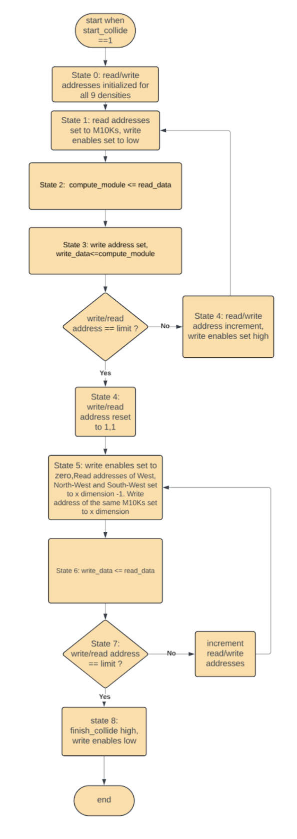
The collision FSM operates in the following way:
- State 0: Read and write addresses initialized for the 9 densities and two speeds.
- State 1: Read address for the 9 densities is set for the first lattice inside boundary excluding boundary. Write enable is set low for M10Ks.
- State 2: Data is read and sent to the compute module to calculate new values of the densities and speeds.
- State 3: Write address is set for all density and speed M10Ks, write data is gotten from the compute module.
- State 4: The write and read addresses are checked, if all desired particles are written, they are set back to the initial condition of the loop and the state goes to state 5. Write enable is set high. If the write address is less than the last value, go back to state 1 after incrementing addresses.
- State 5: Write enable is set to zero. Read addresses of West, North-West, and South-West set to the column just before the right boundary of the lattice. Write address of the same M10Ks set as the right boundary of the lattice.
- State 6: Data copied from the second last column to the right boundary to make fluid flow outward from the lattice to conserve mass in the lattice.
- State 7: Check the read/write address, if reached end of columns, go to state 8 otherwise go to state 5 after incrementing addresses.
- State 8: Set finish_collide signal high and write enables as low.
Stream FSM
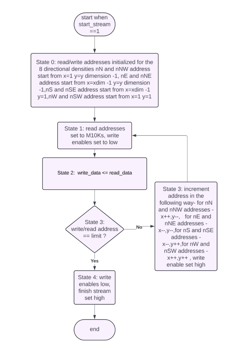
The stream FSM works as follows:
- State 0: The read and write addresses of the 8 directional densities (null not streamed) are set to their initial values.
- State 1: The read and write addresses are set. Pull write enables low.
- State 2: Data is read from the read addresses and copied into the write data of the write addresses of the M10Ks respectively.
- State 3: The read and write addresses are incremented in the following manner: The Addresses for West and South-West start from the South west corner of the lattice traversing rightward horizontally and upward vertically while copying W and SW density values to the adjacent cells. The Addresses for North and North-West start from the North west corner of the lattice traversing rightward horizontally and downward vertically while copying N and NW density values to the adjacent cells. The Addresses for East and North-East start from the North-East corner of the lattice traversing leftward horizontally and downward vertically while copying E and NE density values to the adjacent cells. The Addresses for South and South-East start from the South East corner of the lattice traversing leftward horizontally and upward vertically while copying S and SE density values to the adjacent cells. The write enables are pulled high. The addresses are also checked for their maximum values, if reached move to State 4, otherwise go back to state 1.
- State 4: Set finish_stream as high and pull write enable low.
Initialization FSM
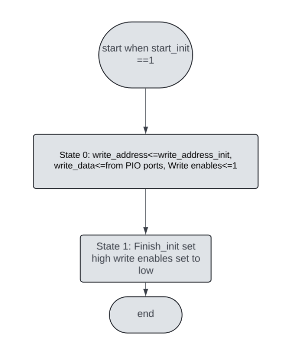
The initialize FSM works as follows:
- State 0: The write address for all M10Ks except color is set equal to the write_address_init coming from the ARM. The data coming from the ARM is put into the write data registers of the M10Ks. Write enables are pulled high.
- State 1: The write enables are pulled low and the finish_init signal is set high.
Move Ship logic and fish multiplexing
The fish co-ordinates are made available to the FPGA through the PIO ports and manipulated on the ARM using ship coordinates sent from the FPGA.
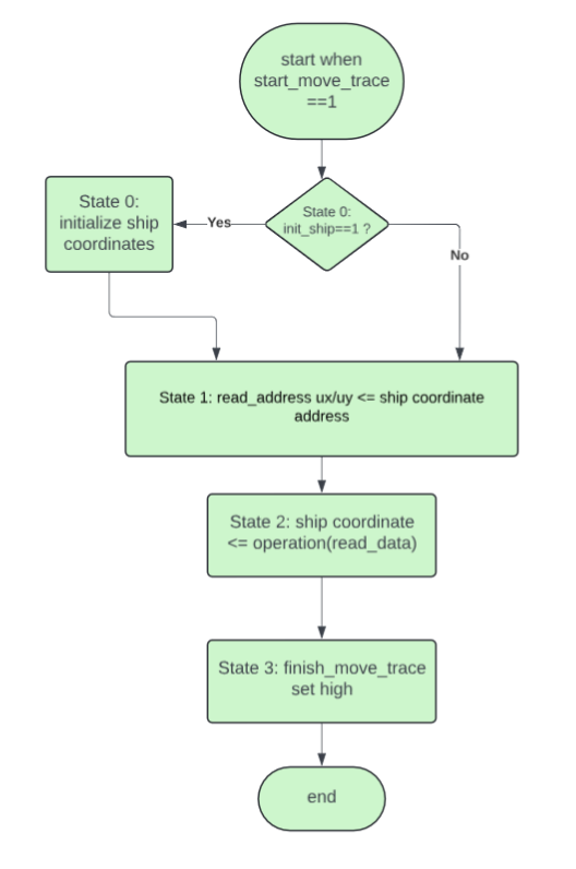
The move ship FSM works as follows:
- State 0: If init_ship signal is turned high from the ARM, initialize ship coordinates to random values.
- State 1: Set read address addresses of speed M10Ks to the address of the particle closest to the ship coordinates.
- State 2: Read speed data and update the coordinates of the ship.
- State 3: Put finish_move_trace high.
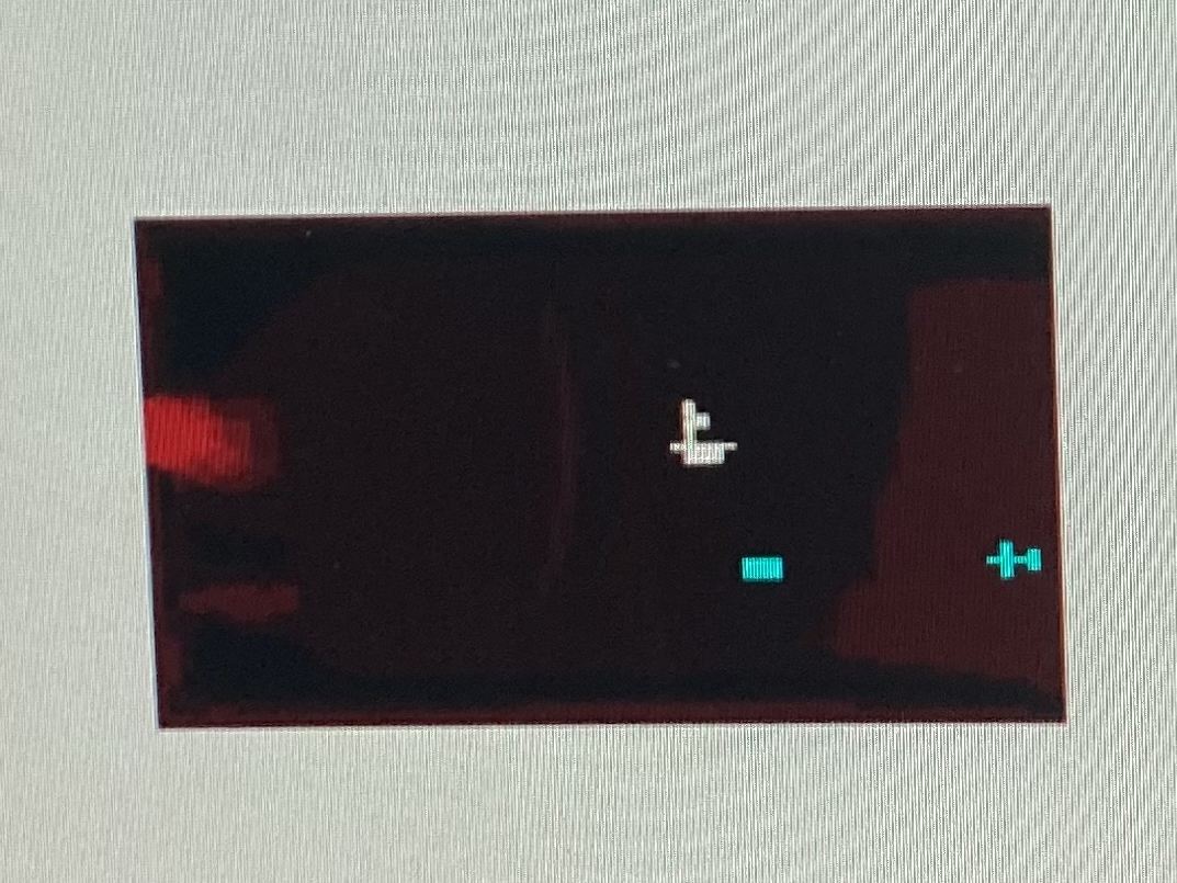
The visual design of the ship and fish is hardcoded by multiplexing the write data of the color data holding M10K, the color data is filled with a constant color around the coordinates of a ship or fish in the shape of a ship or fish.
Update VGA color data FSM
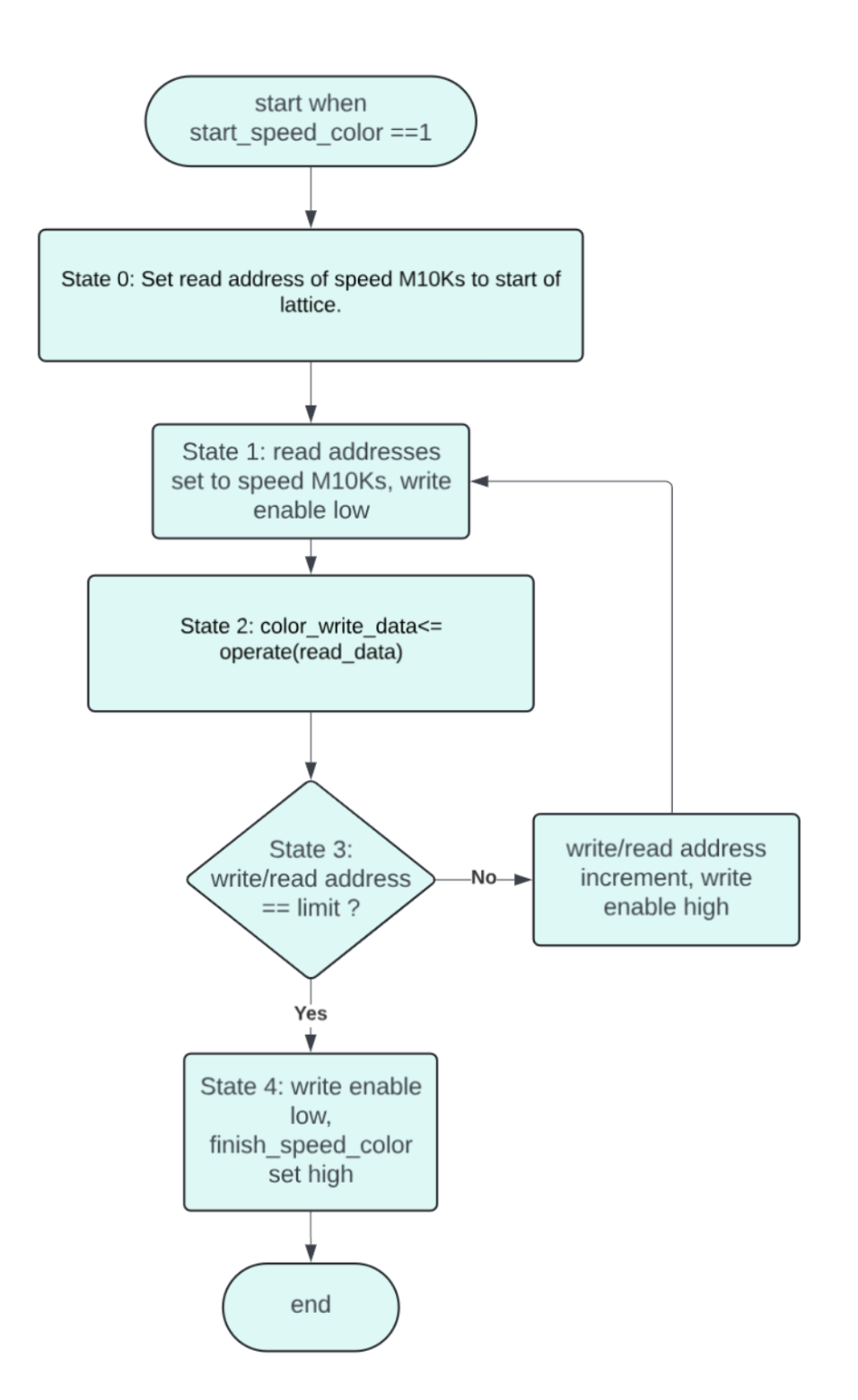
The Update VGA color data FSM works in the following way:
- State 0: Set read address of speed M10Ks to start of lattice.
- State 1: Set read address of speed M10Ks.
- State 2: Read the speed data in x and y direction and compute average speed. Then use the average speed to compute the color given to that cell. Set write address the same as read.
- State 3: Pull write enable high, increment read and write address, check if all particles written. If all written, go to state 4; otherwise, go back to state 1.
- State 4: Put finish_speed_color signal as high and write enable as low.
Memory multiplexing and VGA driver
The color data M10K is written only by the color_VGA FSM and read only by the VGA driver. Since the M10K blocks offer full dual port SRAM with concurrent read and write allowed, the system works well without the need for any synchronization.
The VGA driver used was a custom VGA driver provided by professor adams. Since the size of the lattice was way smaller than the size of the entire screen due to memory limitations, the rest of the screen was multiplexed to a constant white color.
Design Tradeoffs
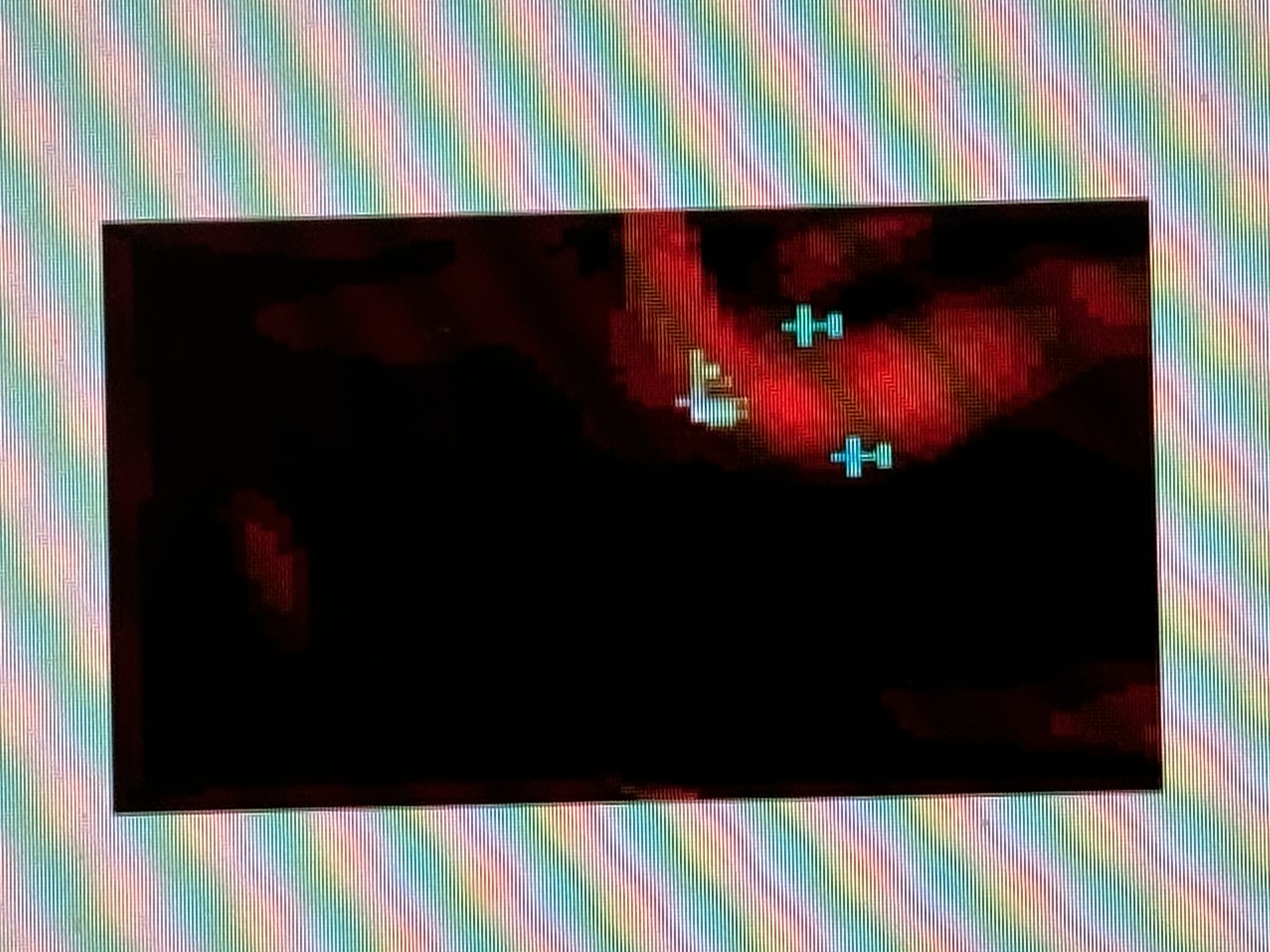
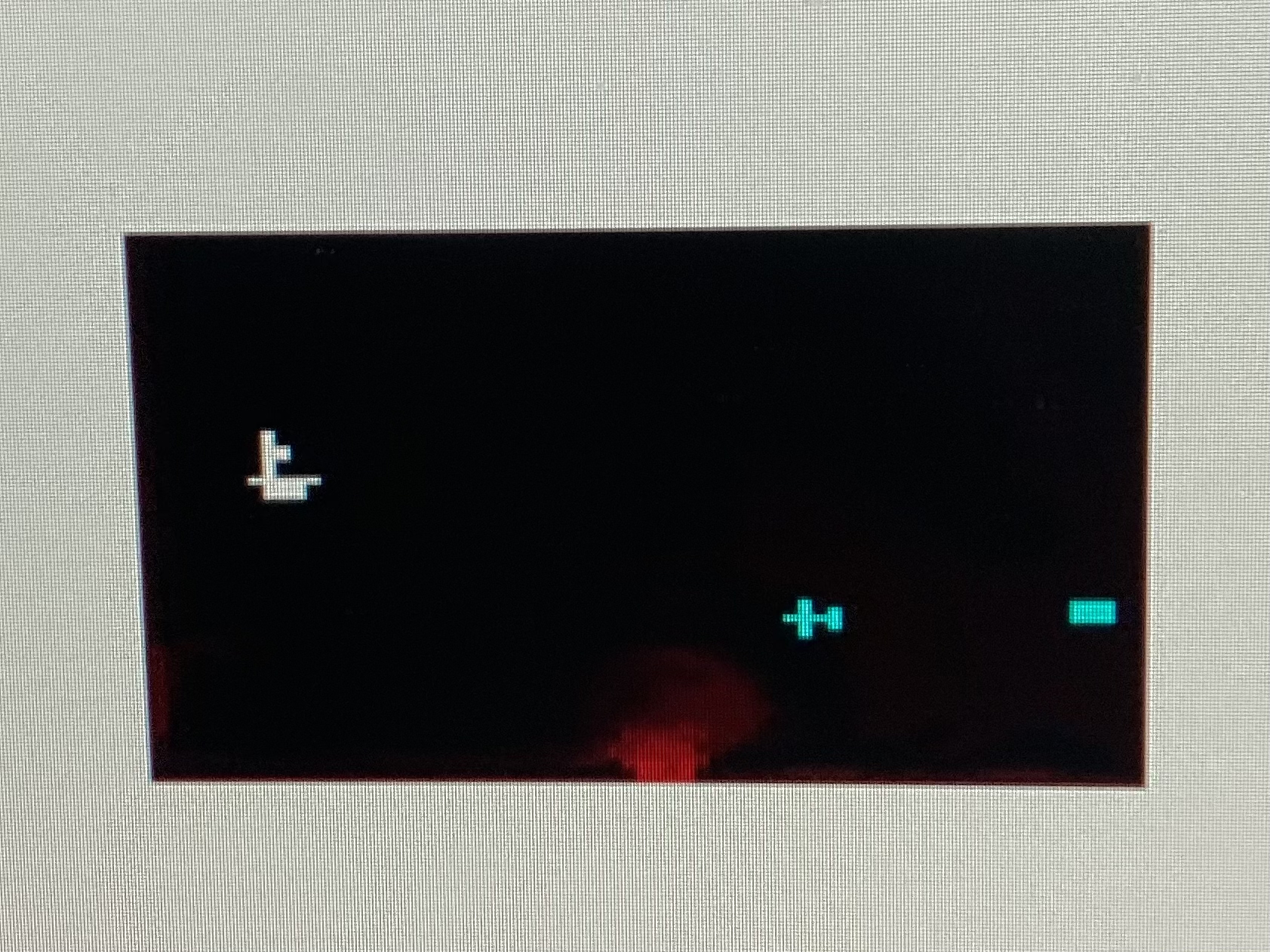
The screen size is reduced due to memory limitations on the FPGA.
8 bit color has to be used instead of 16 bit for the same reason making the color gradient more coarse.
The acceleration reached by the hardware implementation is way more in this approach reaching x53 as compared to the ARM code even without pipelining the read and write. The speedup is gained due to the following reasons- 1) The main bottleneck which was the memory access is now faster as access time for On-chip Sram is way faster than the Off chip SDRAM. 2) The memory of all 13 M10Ks can be read and written parallelly as opposed to serially in the SDRAM due to block division. 3)Computation takes less time in hardware with exploited parallelism and in this approach no time is lost in communicating the computation with the ARM.
Note: The acceleration was so much better that in order to make the game more playable we had to give a 1000us delay between loop iterations using the ARM.