Accelerated Matrix Multiplier
Spring 2024
A Project By Nikhil Mhatre (nm664), Spencer Davis (sd954), and Aditya Acrot (as3745).
Demonstration Video
Introduction
The goal for our final project was to perform accelerated matrix multiplication through the FPGA hardware. We chose to visualize the matrix multiplication through the rotation of a point cloud for the x, y, and z-axis. Matrix multiplication was optimized on the FPGA through an efficient matrix multiplication module and the parallel hardware architecture. We began with initializing 1 SRAM with 300 random pixel coordinate points and grew the project until we reached 15 SRAM with 4500 random pixels. We generated two point clouds on the VGA display, one calculated by the HPS and the other came from the FPGA. Finally, we implemented switch controls for the FPGA display so that we could change the rotation along the x, y, or z axis.
The HPS’s role in the lab was to initialize the SRAMs with random pixel values and print the pixels to the VGA screen. The HPS’s output values were sent to the FPGA through PIO ports set up using Qsys. In Qsys, the PIO ports were assigned unique memory addresses where the data would be stored.
The FPGA was primarily responsible for reading the SRAMs and performing the matrix multiplication with the rotation matrix. We also initialized the SRAMs through the platform designer so that we could set up memory to store the coordinates that the HPS used to print from. Finally, the FPGA switches were used to control the axis of rotation.
Design and Testing Methods
Fixed Point Arithmetic
Fixed point allows the user to perform computation with fractional values and costs less hardware resources than implementing a floating-point data type. The fixed-point value we used in this project was 12.15, corresponding to 12 integer bits and 15 fractional bits. Fixed point values can be added and subtracted without any alterations, but multiplication requires more attention to the location of the decimal point. If we had to multiply two 12.15 signed numbers, we would output a 54-bit number. Since we want to keep a 27-bit number format, the decimal would fall after bit 29, the fractional bits would be [29:15], integer bits would be bits [40:30], and bit 53 would be the sign bit. All the bits above and below would be considered as overflow and underflow, respectively.
Accuracy
With 12.15 fixed point arithmetic, we are limited to +4096/-4096 and a delta of 2-15. Additionally, utilizing the 12.15 fixed point format for our arithmetic allowed us a single DSP module per multiplication since the FPGA multipliers are formatted for either two 18-bit multiplications or a single 27-bit multiplication. Since we knew that DSP blocks were not a bottleneck, we decided to use a higher precision for the results to be as close as the HPS value. This allows us to maximize our DSP usage, allowing 4 DSP blocks matrix multiplication modules.
SRAM Setup
To save the coordinate data that we are constantly updating after computation we decided to implement the on-board SRAM. This is a shared memory between the FGPA and the ARM processor that acts similarly to a M10K block. We set up the SRAM through the platform designer and made sure it was writable, dual port, and established a 32-bit data width with 4096 bytes of total memory. Additionally, we added a clock bridge at 50 MHz that runs the SRAM and the state machine in Verilog. With 4096 bytes of memory, we were able to store 300 pixel points as coordinates for each SRAM and maxed out at 15 SRAMs and 4500 pixel points.
Matrix Multiplication Computation
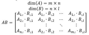
The traditional matrix multiplication is a series of dot products. For matrix multiplication to happen the column of the first matrix must be the same dimension as the rows of the second matrix. A dot product is the sum of the products of a certain row and column in the matrix and is used to solve for the final product matrix. This process for two 3x3 matrices will require 27 total individual multiplications for 3 for each index of the output product matrix.
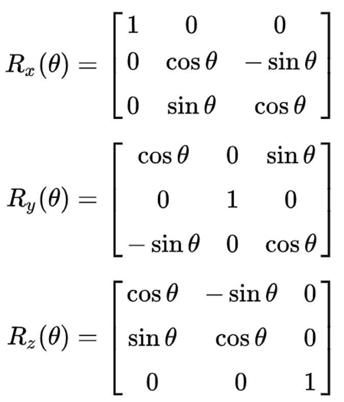
Rotation Matrices
Rotation matrices are transformation matrices that can rotate Cartesian points in the xyz plane. For each axis, there is a set rotation matrix that will rotate points about the x, y, or z axis. θ is the angle at which the rotation matrix will rotate the points about the axis. With matrix multiplication a point defined by the x, y, and z value in a 1x3 matrix can be multiplied by any of the three rotation matrices shown below to shift the point about the desired axis. For rotation matrix multiplications 9 unique multiplications are being performed for each output product matrix due to some values being held constant.
Matrix Multiplication Testing
To test our matrix multiplication modules, we initially developed a base module with a testbench on modelsim. The first module performed 9 multiplications and used 12.15 fixed point representation for our hardcoded initial coordinates, sin(1), and cos(1). After getting the correct output we realized we could rewrite the module using conditional statements to reduce the number of multipliers used down to 4. This is due to the fact that all the rotations were performed about either one of the axes. Which as we can see in the rotation matrices above, fixes 4 of the values to 0 and 1 of the values to 1. We also realized that as we switch from one axis to another the only change is observed in positions of sin and cos. This meant we could use conditional statements to allow a single matrixmul module to switch between axes based on a select signal. We finalized the new matrix multiplication module with conditional statements and 4 signed multipliers and verified the output so we could implement it on the FPGA. This will be explained in further detail in hardware documentation.
High level design
Hardware Design
Below is a listing of the modules and their functions in our Verilog program.
| Name | Description |
|---|---|
| DE1_Soc_Computer | This top-level module contains all the I/O of the FPGA. |
| matrixmul | Takes the initial x, y, z coordinate value, checks the sel bit to perform the corresponding rotation along a particular axis, and outputs a new x,y,z value. |
| signed_mult | Takes the coordinate point, multiplies it by sin or cos determined by matrixmul, and outputs the calculated value. |
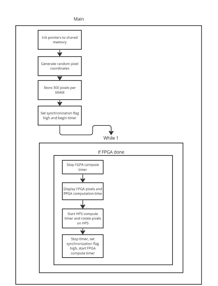
Hardware Flowchart
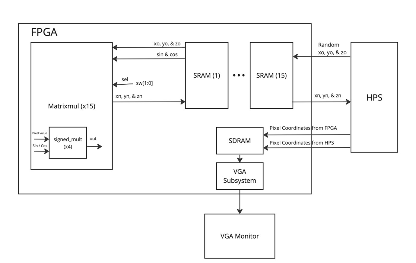
The diagram above shows a detailed data flow between the FPGA, the HPS (ARM), and external outputs utilized in our matrix multiplication accelerator. HPS randomly sets our initial values for the coordinate pixels point clouds. At the start, the point cloud coordinate points are saved into the FPGA’s SRAMs, and the data is organized into each of the 15 SRAMs using their associate base address set in the platform designer. In each SRAM the first address is used for the synchronization signal between the FPGA and HPS. The three next addresses are then used for storing the x, y, and z coordinate values.
Once the 15 SRAMs are initialized the 15 associated matrix multiplication modules along with the SRAM state machine are used to read the coordinate values and assign the associated signals for multiplication. The matrix multiplication is done with 4 signed multipliers and conditional statements that use the switch value to understand which multiplication to perform for a certain axis. When the switches are set to 00 the matrix multiplication of the coordinate point with set rotation matrix for the y-axis will occur, when it is 01 then x-axis rotation will occur, and finally 10 then z-axis rotation will occur. Once the matrix multiplication modules perform the computation the synchronization signal is used for timing and the HPS calculates how fast we completed the multiplication. Finally, the values are written back to the SRAM at the same address. We utilize a generate statement to create multiple matrix multipliers and state machines, so each multiplier module reads and writes into its own SRAM. This allowed for our multiplications to be parallelized and achieve a faster computation time than HPS.
Then the HPS reads the values from the SRAM so that it can calculate the coordinate points to draw to the VGA monitor. On the HPS side, we are also performing matrix rotation multiplication with the same number of pixels and outputting them to the VGA monitor so we can have a side-by-side display of the FPGA and HPS points and their corresponding computation time. Additionally, HPS formats the colors of the pixels based on the z-coordinate values, so it fades the further away the pixel goes into the screen. The coordinate points from the FPGA and HPS are both sent to the SDRAM which is utilized by the VGA subsystem to finally output our two point clouds simultaneously.
One issue we faced when implementing more SRAMs was due to the increasing critical path that caused our read to be more than a single cycle. We had initially written the Verilog code to pipeline reads for x, y and z coordinates and then pipeline writes for the new x, y and z coordinates. But as we started increasing the number of pixels and SRAM size, we noticed that our program kept failing at various stages. Initially, we were able to perform single cycle reads, but when we started experimenting with 10 SRAMs, we had to modify our verilog to allow 2 cycle reads and writes. Regardless, this only affected the latency of our program by 1 cycle per pixel transformation due to the pipelining of our code.
Qsys Layout
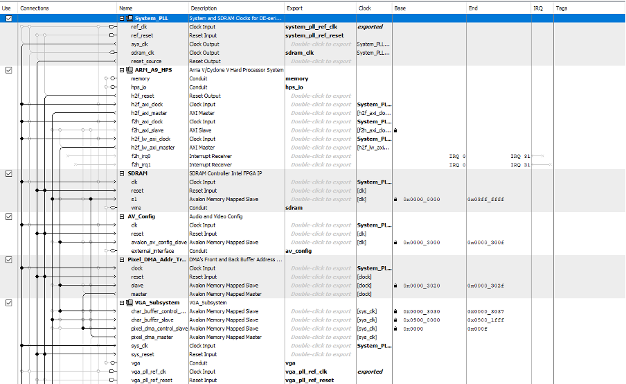
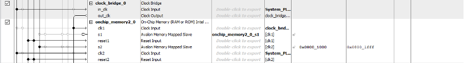
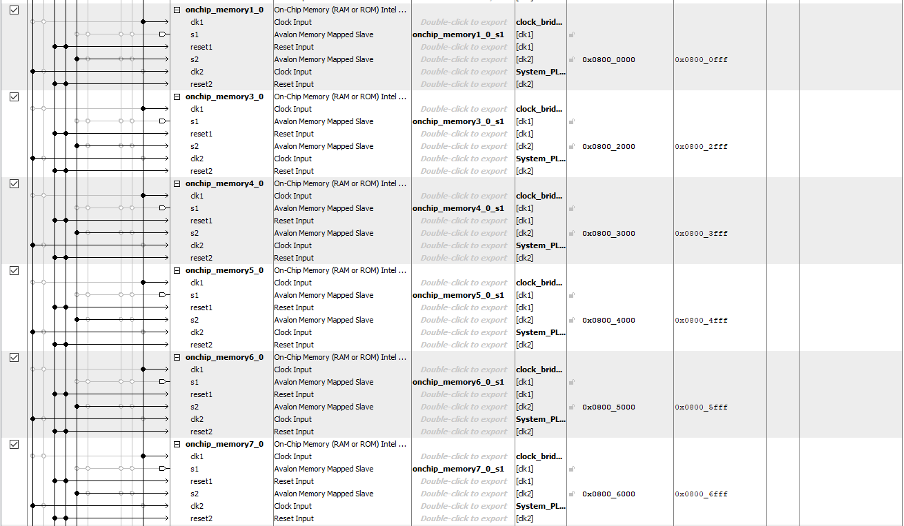
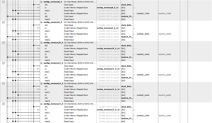
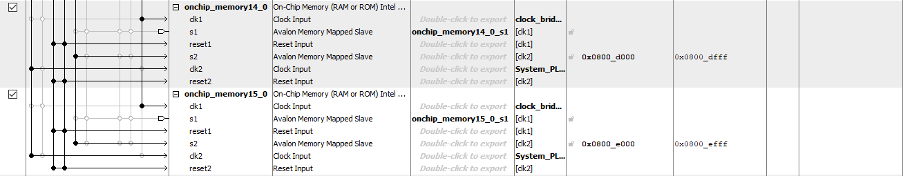
QSYS uses a graphical interface to easily connect and configure pre-designed intellectual property (IP) blocks, such as processors, memory controllers, and peripherals. As shown above, in the layout diagram, we added 15 SRAM on-chip memory to communicate between the HPS and FPGA. The 15 SRAMs were all connected to the lightweight AXI Bus and were addressed not to overlap. Once all the SRAMs were added and addressed, we double-clicked the conduit connection's export option. This makes all the s1 signals external to the module, which can then be accessed in the Verilog file. All the SRAMs were also clocked at 50 MHz through the clock bridge also set up in Qsys.
Software Description
Below is a table detailing the functions and variables used in our HPS program.
| Name | Description |
|---|---|
| main() | This function maps pointers to each SRAM utilized by our matrix multiplication modules. It fills each module with 300 random pixel coordinates. It also initializes the rotation matrix. In the main while loop, the program waits until the zeroth matrix multiplier module signals that it is complete. Signaling is done using the first index of the SRAM. If the value in the associated SRAM is a zero, that means that the HPS is working on the data, if the value is a 1, That means that the FPGA is working. When the C program reads that it is its turn to operate on the data, the HPS stops a timer, calculates the time that the FPGA was working on the data, and plots the FPGA calculated points on the screen. It then starts a timer and begins multiplying the rotation matrix it calculated earlier to each pixel location. A timer is started before this process and is finished once the points are all updated. This time is shown on the screen. At the end of the loop, the HPS sets each of the SRAM's first indices to 1 indicating to the FPGA that it can begin calculating its values. This process loops indefinitely. |
| rotMatrix | This is a rotation matrix calculated based on a desired rotation angle per update. Our program rotates a pixel 1 degree per frame. |
| Vectors | This matrix of Vector structs contains an entry for each pixel. The values are initialized to a random value. |
| FPGA(X/Y/Z)OLD(X) | Each SRAM is given an associated array of old values. Since we don’t want to clear the entire screen when updating points and would just like to erase each point individually, we must store the old coordinates so we can erase the old point before drawing a new point at the coordinate specified by the FPGA. |
| rotate_y() | This function generates a rotation matrix about the y-axis. |
| rotateVector() | This function does our matrix multiplication and rotates a given vector by multiplying it with a rotation matrix. |
| getRandomFloat() | This function gets a random floating-point value between two limiting values. We chose the limiting values to be -60 and 60. This results in the point cloud showing as a cube. |
| getRandomVector() | This function returns a random Vector struct containing a random x,y, and z coordinate. |
| DEG2RAD() | This macro converts an angle from degrees to radians. |
| FRAME_RATE | This macro defines the number of microseconds to sleep to keep a 60fps update speed to the VGA. The sleep does not effect measured computation times. |
| NUMOFMULT | This macro defines the number of multipliers that exist on the FPGA. |
| numOfRows/numToDisplay | These equivalent macros define the total number of pixel points that exist on the FPGA and the HPS. |
HPS Program Flow
Above is the general flow of the HPS program and each major step completed by the HPS. The program starts by initializing pointers to the start of each SRAM block. We initialize random coordinates and populate both the HPS memory and FPGA SRAM memory. We set a synchronization signal high indicating to the FPGA that it can begin operating on that data. Just before we do that, we have started the timer responsible for counting the time between when the FPGA starts operating on data and when it finishes. In our main while loop, we have a single if statement waiting for that synch signal to indicate that the FPGA is done. Once the FPGA is done, we stop our timer. We then go through the process of getting the x y and z coordinates. We plot the pixel at the x and y coordinate, and we use the z coordinate to get the color of the pixel. We then move to the HPS calculated coordinate. We rase the current pixel location, perform a matrix multiplication, and draw the pixel at its new location. We then display the time for it to do so. Lastly, we set the FPGA synchronization signal to let the FPGA know it can begin calculating new positions and we start a timer. The process loops until the user quits the program.
Depth Visualization
When displaying a point cloud on the VGA, we wanted to indicate to the user the z depth into the screen. One way we could do this would be to draw pixels in a sorted manner. We could draw pixels in an order corresponding to their depth into the screen from farthest away to closest. This works quite well, but a better way to display depth would be to color the pixels based on their depth. The VGA driver uses a 16-bit color for each pixel. This means that for each pixel, 5 bits are dedicated to red, 6 to green (since humans can see variation in green the best), and 5 for blue. If we set each R, G, and B component equal, we can get different shades of the same color. We can use the following formula to calculate color:
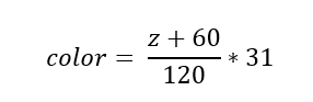
Where 60 is the minimum value of each vector component, 120 is the range (-60 - 60) and 31 is the maximum value of the smallest bit width of color (ie2^5-1). If, for example, the vector’s z component was extremely far away at -60, plugging into this equation, we result in zero. The color zero is black and the pixel is not seen. If you scroll down this webpage and look at the images of the rotating point clouds that we rendered, you will notice that the pixels are not grayscale and instead have a pink'ish color. We have no idea why this is happening, and upon evaluation of the color output of a random pixel and its associated color, we should be seeing some shade of gray.
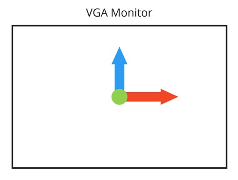
VGA Coordinate Frame (pixels further away sink into the screen)
Results
Pixels Rendered |
SRAMs Utilized |
HPS Compute Time (us) |
FPGA Compute Time (us) |
|---|---|---|---|
50 |
1 |
286 |
7 |
300 |
1 |
1600 |
42 |
600 |
2 |
3200 |
42 |
1500 |
5 |
8190 |
42 |
3000 |
10 |
16070 |
42 |
4500 |
15 |
23500 |
45 |
FPGA vs HPS Implementation Time Comparison
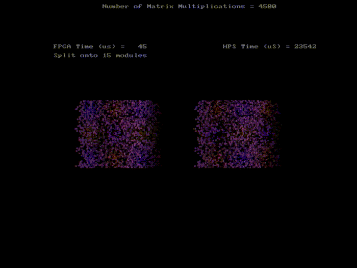
4500 pixels rotations with 15 SRAMs
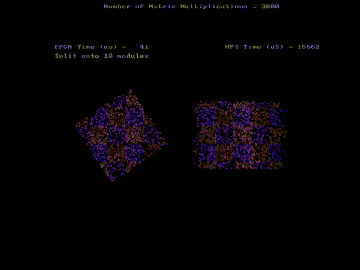
3000 pixels rotations with 10 SRAMs with variable axis rotation
We successfully developed an optimized and accelerated matrix multiplication module in Verilog. Our HPS implementation does 9 separate multiplications with the rotation matrix and requires multiple cycles for each multiplication. On the other hand, our FPGA module uses 4 multipliers for performing matrix multiplication and can transform one pixel per cycle. As shown in the table above we were able to successfully implement 15 SRAM modules which allows us to do 15 pixels in one cycle. Ideally, with 15 pixels per clock cycle and a 50 MHz clock, we would be able to transform 750,000,000 pixels. From the data, we can see that 4500 pixels takes 45 us which equates to 100,000,000 pixels transformation. Since we used the ARM for reading and writing into our SRAMs, we had to wait for each read and write for all 3 coordinates. This resulted in a 7-cycle latency, 3 for read, 3 for write, and 1 for computation.
Conclusion
The project exposed the power of parallel hardware architecture for accelerating computationally intensive tasks. We improved the matrix multiplication method to 4 multipliers compared to our HPS implementation with the help of conditional statements. To visualize the matrix multiplication, we used the set rotation matrices to rotate a point cloud and output the FPGA and HPS calculations to a VGA screen. Our final FPGA hardware design rendered 4500 points in 45us while the HPS took 23500 us with 15 SRAMs. We used switches to rotate the points clouds around all three axes but could only render the points with 10 SRAMs. We met our acceleration expectation and believe next time we can further optimize the number of DSPs used with a smaller fixed-point representation. We also faced issues printing our pixel to the VGA monitor once we went above 15 SRAMs due to the critical path to write back taking longer than 1 cycle. This resulted in pixel point cloud display randomly drawing to the screen and was a limiting point in our project. Our matrix multiplication module was originally developed by our team. We got assistance from Professor Hunter Adams's On-Chip SRAM lecture video to learn how to set up the SRAMs on platform designer and write the associated state machine in Verilog.
Team


Appendices
The group approves this report for inclusion on the course website.
The group approves the video for inclusion on the course youtube channel.
Download matrix multiplier ZIP File