Introduction(To Top)
Our goal is to design a polygonal rasterizing graphics processing unit on the Cyclone V SoC.We developed a basic render pipeline with hardcoded vertex/fragment shaders which works in simulation. The render pipeline consists of vertex transformation, triangle tiling, triangle rasterization/interpolation, fragment transformation. We also developed a grid of parallel SIMD processor cores which supports 4 word vector operations and 16 word matrix operations. The SIMD processors also support performing simultaneous multithreading allowing for 2 independent thread contexts to share compute resources. The processors are planned to be used to replace the haredcoded vertex/fragment shaders in the render pipeline. For use in both the rendering and the SIMD processor is a 27-bit floating point library designed to perfectly utilize the 18-bit hardware multipliers. To help verify the design, we also setup a basic UVM framework to facilitate testing.
High Level Design(To Top)
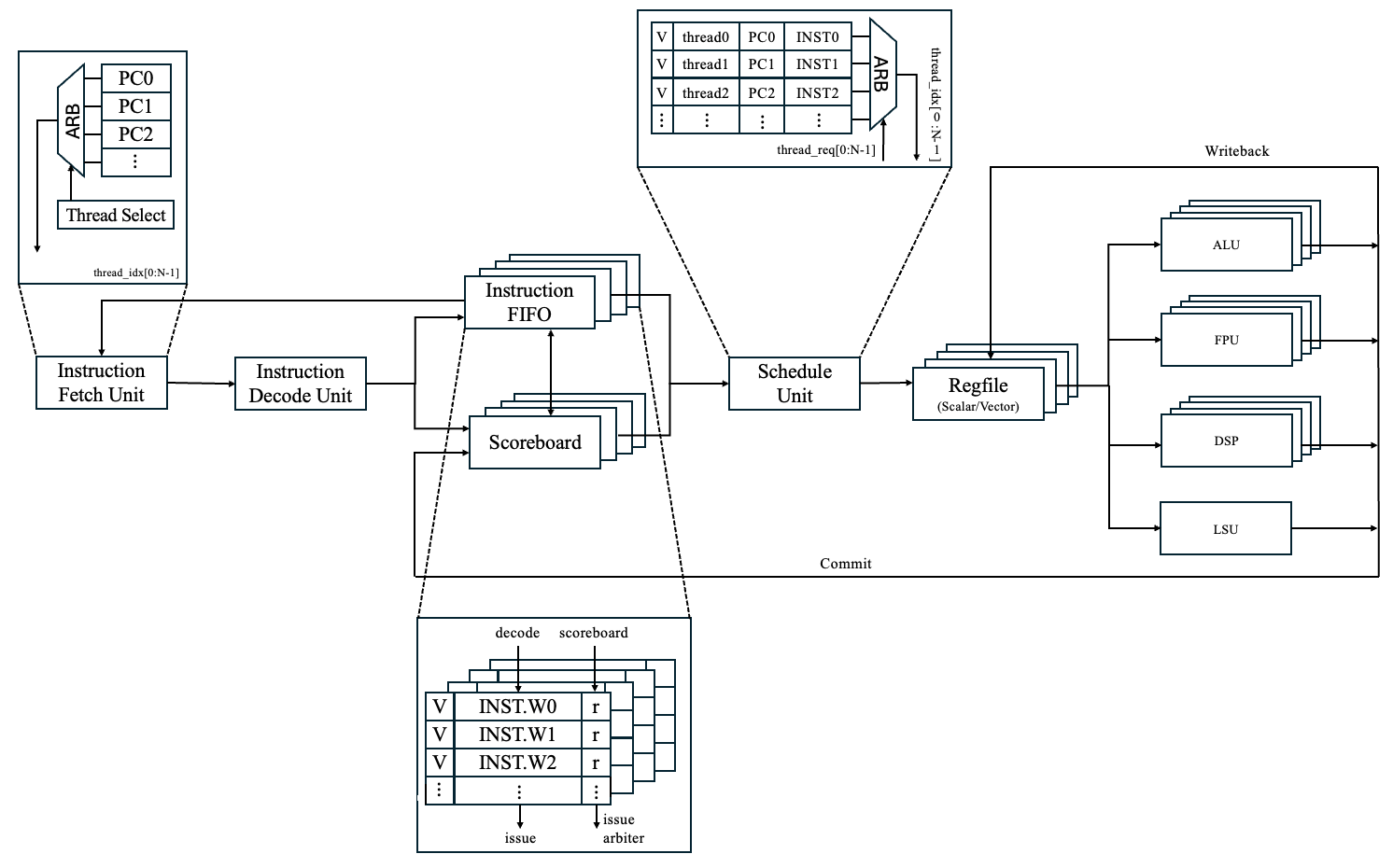
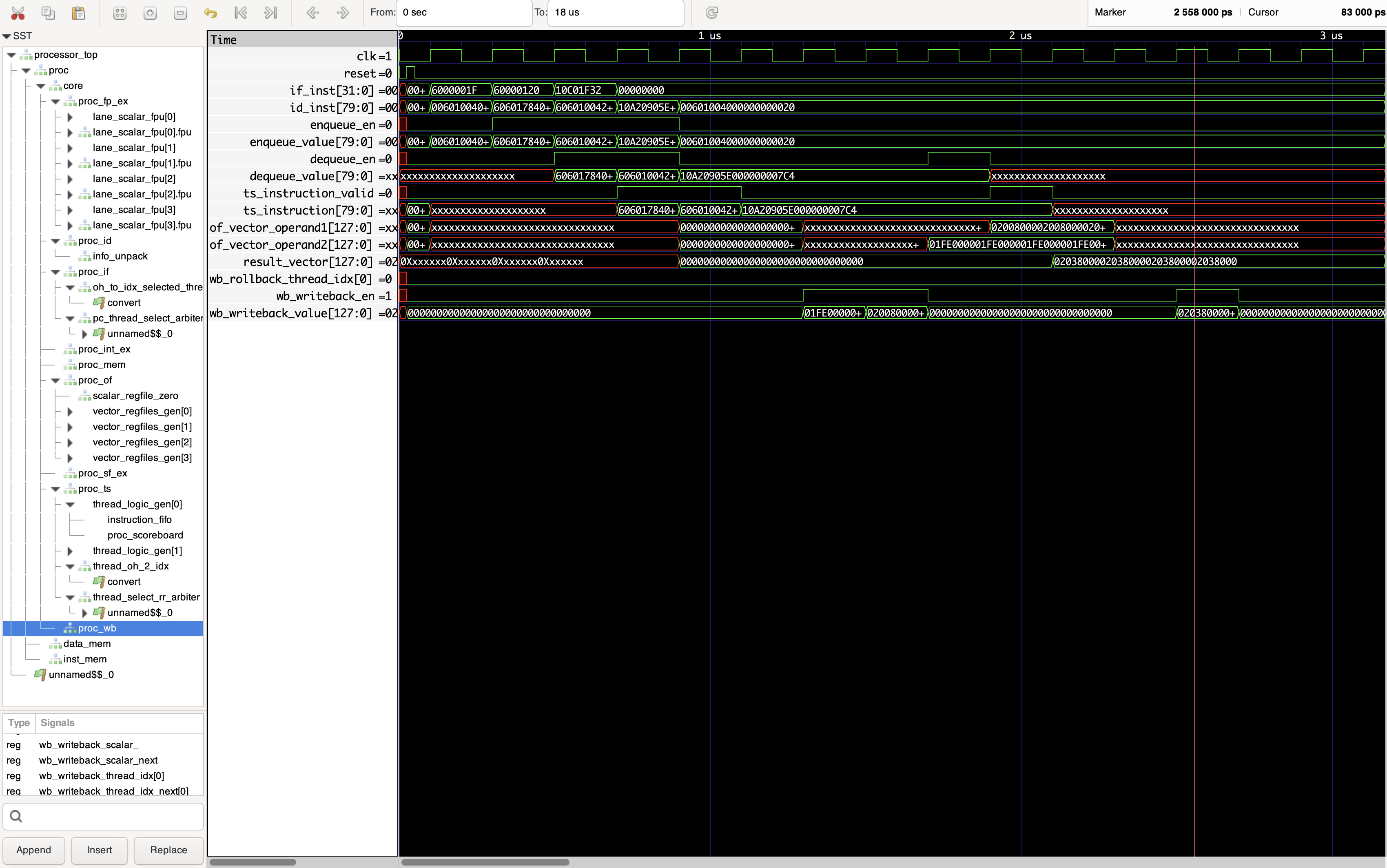
SIMD Core Execution Pipeline
Each core of the processor is equipped with multiple hardware threads, which to software applications, function as independent processors, complete with their own program counters and sets of general-purpose registers. Despite their independence in operation, these threads share critical resources such as the arithmetic pipeline and L1 caches within their core. The primary objective of this multithreading approach is to maximize the utilization of these shared resources. When a thread encounters a stall caused by a cache miss or a data dependency, the core has the capability to switch operations to another thread, ensuring continuous execution. The core systematically aims to cycle through and issue instructions from various threads each cycle whenever feasible.Should an instruction trigger a data cache miss, a branch, or an exception, the core responds by invalidating any subsequent instructions issued by the affected thread. In the case of a branch, the program counter is reset to the destination of the new branch, and execution continues from that point. When a cache miss occurs, the corresponding thread is temporarily halted until the necessary data is fetched by the memory subsystem, at which point execution resumes from the point of interruption.
This processor architecture includes 16 parallel arithmetic pipelines, each aligned with one of the vector lanes, enhancing its capacity for handling vectorized data. Scalar operations utilize only the first pipeline, while instructions involving both scalar and vector operands are facilitated by duplicating the scalar values across all lanes. Moreover, instructions have the flexibility to specify updates to particular vector lanes through a mask register, allowing for selective and efficient data processing.
Designed with a deep pipeline, this processor achieves a higher clock speed, optimizing performance. Illustrated below is a diagram depicting the execution pipeline for a single core, outlining the intricate stages and processes involved in the data flow and instruction handling within the core.
Render Pipeline (Initial)
Our initial plan of a GPU is to have the SDRAM store all the information of the 3D models as well as the 2 framebuffers storeing their respective color and depth buffers. This allows us to do double buffering and prevent screen tearing. The cross shaped router directs SDRAM memory reads and writes between the VGA and the rendering pipeline to allow them both to share a single port. A depth cache is used to keep the recently used depth values and reduce memory reads/writes to the SDRAM, while all color values are written to SDRAM as it is not likely stall the pipeline. In the end significant changes had to be made to the design both due to physical resource constraints and time constraints.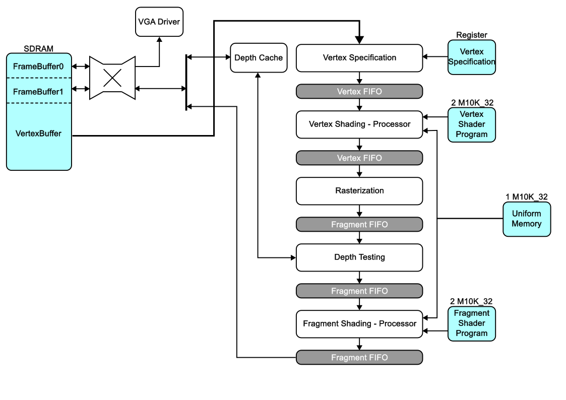
Rasterization Rendering
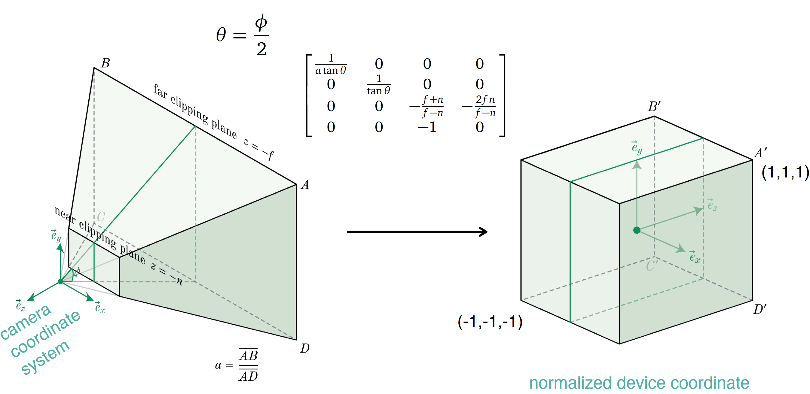
The purpose of rasterization rendering is to take some collection of data and transform it into a grid of pixels. In our case, the data is a collection of 3D vertices for which every 3 vertices are organized into an independent triangle. To help us work in this space we use homogeneous coordinates which expands the conventional linear transform to include a nonlinear translation component. In homogeneous coordinates, vectors are composed of 4 terms (x,y,z,w) where if w=0 it is considered a 3D vector and if w=1 it is a 3D point.
Projective Geometry
To render our image we define a flat surface, our screen, and project the objects in our scene onto said surface. To standardize calculations, we can define a surface from (-1,-1,z) to (1,1,z) and imagine linearly transforming some space of everything that is visible from our perspective (x0, y0, z0) to (x1, y1, z1) down to between (-1,-1,-1) and (1,1,1). This is called the normalized device coordinates and introduces a notion of a near and far clipping plane as if we only render the pixels that land between (-1,-1,-1) and (1,1,1) we can never see closer than z0 or farther than z1.However, if we simply projected all of our objects onto said flat surface, objects would look to be the same size regardless of distance. This is called orthographic projection which is useful for blueprints or CAD but does not accurately represent the way human eyes perceive the world. To achieve a realistic perspective in our rendering, we have to make it so that distant objects look smaller. We do this by not transforming a rectangular prism but instead a rectangular frustum. As such, the more space closer to the far clipping plane would be compressed into the same square as less space closer to the near clipping plane, giving the illusion that distant objects are smaller.
 UCSD CSE 167 Lecture Slides
Triangle Rasterization
We chose an edge-function based method for triangle rasterization. The basic idea is that the 2D cross product between a vector representing a line and the vector from the line to some point p results in the signed-area of the parallelogram formed from the 2 vectors. The sign would be positive if p is on one side of the line and negative on the other side. By defining the positive side as "inside" and checking with all 3 sides of the triangle we can determine if any given point is inside of the triangle by checking if the signed-areas are all positive. This cross product is called the edge function as it can be used to determine if a point is on one side or the other side of an edge. The edge function has an advantage of being linear, making it easy to iterate across unit displacements using only addition and subtractions, saving on hardware multipliers. Another advantage here is that "back-facing" triangles will have all negative areas when inside allowing us to quickly skip over them and save on computation.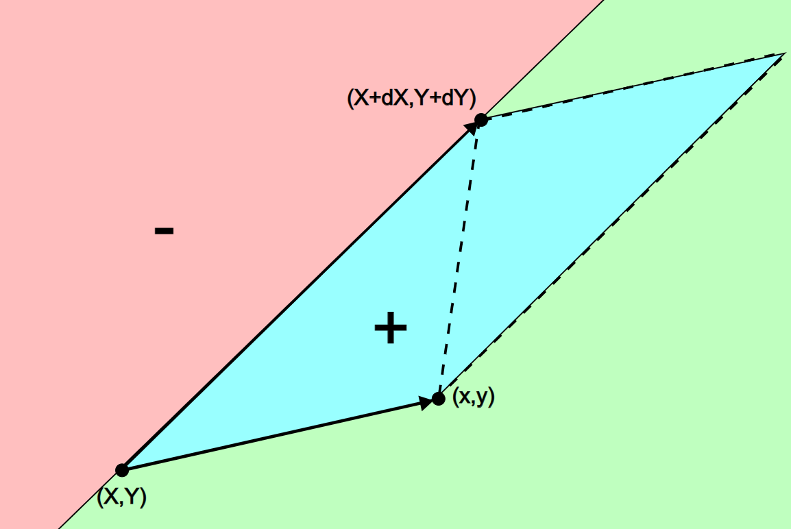
 For interpolation, we utilize barycentric coordinates to weigh each attribute of the vertices appropriately. The barycentric coordinates are also equal to the ratio of the sub triangles formed by each edge and the point p to the full triangle. As such, we can use the area computed above (parallelogram has double the area of the sub triangles) to compute the barycentric coordinates.
Perspective Correction
Before we can do interpolation we must first do perspective correction on the barycentric coordinates. This is because the current barycentric coordinates are linear on the screen surface which does not take into account the depth of the triangle. The correction can be applied by weighing each barycentric coordinate by the inverse depth of its vertex (or directly with the product of the depth of the other 2 vertices). Finally, the interpolated attribute at any point is the sum of the attribute from the 3 vertices weighted by the perspective corrected barycentric coordinates.
Depth Testing
Another key aspect of rendering is that closer objects can occlude farther ones. If we simply process all triangles received in the same order, it is possible for a farther triangle to be processed later and cover the closer triangle rendered earlier. While it is possible to sort the triangles from farthest to closest or require the input be already sorted, this leads to an annoying issue if some parts of triangle A occlude triangle B and at other parts B occludes A (like if the triangles intersect).A far more common and straightforward solution is to just store the depth of the closest pixel that has been rendered and discard pixels whose depth is behind the closest pixel. This method is called depth testing which for every pixel stores the depth into a depth buffer if it is closer than depth currently stored at that location. This does however strain our already limited on-chip memory as we now need to store both the color of said pixel and the depth. We resolve this by off loading the bulk storage to the SDRAM and using on-chip memory like a cache.
Design Constraints/Tradeoffs
Memory Constraint
As briefly mentioned in the depth testing section above, our on-chip memory is quite limited. With there not even enough memory to store 16-bit color for a 640x480 screen, we are forced to either reduce the scale of the screen or tap into the off-chip SDRAM to store the necessary data. We chose to use the off-chip SDRAM for bulk storage and the on-chip memory as cache.To facilitate this, we organized the color/depth buffers into tiles of 32 x 32 pixels which can be moved between SDRAM and on-chip cache for rendering. The choice of 32 x 32 is so the screen can be evenly distributed across 20 x 15 tiles while the choice of tiles is because we want to have 2D spatial locality. The memory is also organized into tiles instead of by rows and columns. Each tile takes up a 4KB of contiguous space where the first 2KB stores the color and the last 2KB stores the depth both with 16-bit resolution. Each tile is then organized contiguously at the top of SDRAM. We also utilize 2 of such buffers to perform double buffering and prevent screen tearing.
Hardware/Program Design(To Top)
Floating Point Processing Unit
We chose to do 27-bit floating point because it would have a 18-bit mantissa which fits quite nicely into the 18x18 hardware multiplier we have on the SoC. This is also convenient for data conversion as the format is just the IEEE 32-bit floating point with the last 5 bits of the mantissa truncated.FpAdd
The basic FpAdd module takes in 2float27 and performs comparison on the value to find the value of smaller magnitude. After doing so, the smaller value is shifted such that both values are aligned in the same exponent before addition is performed. After addition, the value is renormalized by counting the number of leading zeros then shifting an appropriate number of bits and adding to the exp part of the float. Finally, a mux checks some conditions on the initial input values to determine if a special value such as Nan or Inf needs to be outputted instead of the computed value. For instance, Inf + Inf = Inf, Inf - Inf = Nan, etc.
FpMult
The basic FpMult module is rather similar to the FpAdd module. The same normalization of the exponents occurs so that both values align in fixed point representation. Then a multiply is performed and normalization occurs with counting leading zeros. Another mux is then used here to potentially swap out the computed value with special values. For instance, Inf * Inf = Inf, a * Nan = Nan, etc.FpAlu
The FpAlu module is one which combines multiple different possible floating point operations. It consists of 1 FpAdd and 1 FpMult module for the ADD, SUB, and MULT operations. The DIV_SQRT operation uses the above 2 modules iteratively to do the fast inverse square root algorithm. The DIV operation does an inverse square root of the divisor before squaring the output and multiplying by the dividend. The ABS simply sets the sign bit to 0 and NEG flips the sign bit.SIMD Processor
Instruction Decode
During the instruction decode stage of the processor, the necessary register operands for each instruction are identified by the decoding logic. This stage meticulously extracts the indices of these registers directly from the instruction data and allocates them to the appropriate ports on the register file. Furthermore, it assigns the instruction to a specific execution pipeline, which is a crucial step in streamlining the processing flow.This stage also plays a pivotal role in the overall execution pipeline by providing essential data to later stages. It helps in tracking the execution path and scheduling of the instruction, which is critical for the efficient management of the processor's resources. Additionally, the information gleaned during the decode stage is instrumental in monitoring and resolving any potential conflicts that might occur during the register writeback process, such as ensuring that no two instructions improperly overwrite each other's results. This careful coordination helps maintain data integrity and consistency across the processor's operations, enhancing both performance and reliability.
fmt format for R type
| fmt | rs2 | rs1 | mask | rd |
|---|---|---|---|---|
| 000 | scalar2 | scalar1 | NONE | scalar |
| 001 | scalar2 | vector1 | NONE | vector |
| 010 | scalar2 | vector1 | scalar1 | vector |
| 100 | vector2 | vector1 | NONE | vector |
| 101 | vector2 | vector1 | scalar1 | vector |
fmt format for I type
| fmt | rs1 | mask | rd | encoding |
|---|---|---|---|---|
| 00 | scalar | NONE | scalar | B |
| 01 | vector | NONE | vector | B |
| 10 | NONE | NONE | scalar | C |
| 11 | vector | scalar | vector | A |
R-Type Instructions
| Instruction Name | Opcode | Description | Bit Encoding Example |
|---|---|---|---|
| INST_VOR | 000010 | Vector/Scalar bitwise OR operation | 000_000010_???_0000_????_????_????_???? |
| INST_VXOR | 000011 | Vector/Scalar bitwise XOR operation | 000_000011_???_0000_????_????_????_???? |
| INST_VADDI | 000100 | Vector/Scalar integer addition | 000_000100_???_0000_????_????_????_???? |
| INST_VSUBI | 000101 | Vector/Scalar subtraction | 000_000101_???_0000_????_????_????_???? |
| INST_VLSL | 000110 | Vector/Scalar logical shift left | 000_000110_???_0000_????_????_????_???? |
| INST_VRSL | 000111 | Vector/Scalar logical shift right | 000_000111_???_0000_????_????_????_???? |
| INST_VRSA | 001000 | Vector/Scalar arithmetic shift right | 000_001000_???_0000_????_????_????_???? |
| INST_VCLZ | 001001 | Vector/Scalar count leading zeros | 000_001001_???_0000_????_????_????_???? |
| INST_VCTZ | 001010 | Vector/Scalar count trailing zeros | 000_001010_???_0000_????_????_????_???? |
| INST_VCPY | 001011 | Vector/Scalar copy operation | 000_001011_???_0000_????_????_????_???? |
| INST_VCMPEQI | 001100 | Vector/Scalar integer compare equal to | 000_001100_???_0000_????_????_????_???? |
| INST_VCMPNEI | 001101 | Vector/Scalar integer compare not equal to | 000_001101_???_0000_????_????_????_???? |
| INST_VCMPSGTI | 001110 | Vector/Scalar integer compare greater than | 000_001110_???_0000_????_????_????_???? |
| INST_VCMPSGEI | 001111 | Vector/Scalar integer compare greater or equal to | 000_001111_???_0000_????????????_???? |
| INST_VCMPSLTI | 010000 | Vector/Scalar integer compare less than | 000_010000_???_0000_????_????_????_???? |
| INST_VCMPSLEI | 010001 | Vector/Scalar integer compare less or equal to | 000_010001_???_0000_????_????_????_???? |
| INST_VCMPUGTI | 010010 | Vector/Scalar integer compare unsigned greater than | 000_010010_???_0000_????_????_????_???? |
| INST_VCMPUGEI | 010011 | Vector/Scalar integer compare unsigned greater or equal to | 000_010011_???_0000_????_????_????_???? |
| INST_VCMPULTI | 010100 | Vector/Scalar integer compare unsigned less than | 000_010100_???_0000_????_????_????_???? |
| INST_VCMPULEI | 010101 | Vector/Scalar integer compare unsigned less or equal to | 000_010101_???_0000_????_????_????_???? | INST_VSUBF | 100000 | Vector/Scalar subtraction (floating-point) | 000_100000_???_0000_????_????_????_???? |
| INST_VADDF | 100001 | Vector/Scalar addition (floating-point) | 000_100001_???_0000_????_????_????_???? |
| INST_VMULF | 100010 | Vector/Scalar multiplication (floating-point) | 000_100010_???_0000_????_????_????_???? |
| INST_VDIVF | 100011 | Vector/Scalar division (floating-point) | 000_100011_???_0000_????_????_????_???? |
| INST_VCMPEQF | 100100 | Vector/Scalar compare equal (floating-point) | 000_100100_???_0000_????_????_????_???? |
| INST_VCMPNEF | 100101 | Vector/Scalar compare not equal (floating-point) | 000_100101_???_0000_????_????_????_???? |
| INST_VCMPSGTF | 100110 | Vector/Scalar compare greater than (floating-point) | 000_100110_???_0000_????_????_????_???? |
| INST_VCMPSGEF | 100111 | Vector/Scalar compare greater or equal (floating-point) | 000_100111_???_0000_????_????_????_???? |
| INST_VCMPSLTF | 101000 | Vector/Scalar compare less than (floating-point) | 000_101000_???_0000_????_????_????_???? |
| INST_VCMPSLEF | 101001 | Vector/Scalar compare less or equal (floating-point) | 000_101001_???_0000_????_????_????_???? |
| INST_VDOTI | 101010 | Vector/Scalar dot product with integers | 000_101010_???_0000_????_????_????_???? |
| INST_VDOTF | 101011 | Vector/Scalar dot product with floating-point numbers | 000_101011_???_0000_????_????_????_???? |
| INST_VIFT | 101100 | Vector/Scalar integer to floating-point conversion | 000_101100_???_0000_????_????_????_???? |
| INST_VFTI | 101101 | Vector/Scalar floating-point to integer conversion | 000_101101_???_0000_????_????_????_???? |
I-Type Instructions
| Instruction Name | Opcode | Description | Bit Encoding Example |
|---|---|---|---|
| INST_VAND_IMM | 000001 | Vector/Scalar AND | 1_??_000001_???????_????_????_????_???? |
| INST_VOR_IMM | 000010 | Vector/Scalar OR with immediate | 1_??_000010_???????_????_????_????_???? |
| INST_VXOR_IMM | 000011 | Vector/Scalar XOR with immediate | 1_??_000011_???????_????_????_????_???? |
| INST_VADDI_IMM | 000100 | Vector/Scalar addition | 1_??_000100_???????_????_????_????_???? |
| INST_VSUBI_IMM | 000101 | Vector/Scalar subtraction | 1_??_000101_???????_????_????_????_???? |
| INST_VLSL_IMM | 000110 | Vector/Scalar logical shift left | 1_??_000110_???????_????_????_????_???? |
| INST_VRSL_IMM | 000111 | Vector/Scalar logical shift right | 1_??_000111_???????_????_????_????_???? |
| INST_VRSA_IMM | 001000 | Vector/Scalar arithmetic shift right | 1_??_001000_???????_????_????_????_???? |
| INST_VCLZ_IMM | 001001 | Vector/Scalar count leading zeros with immediate | 1_??_001001_???????_????_????_????_???? |
| INST_VCTZ_IMM | 001010 | Vector/Scalar count trailing zeros with immediate | 1_??_001010_???????_????_????_????_???? |
| INST_VCPY_IMM | 001011 | Copy vector elements with immediate | 1_??_001011_???????????????????_???? |
| INST_VCMPEQI_IMM | 001100 | Compare vector/scalar elements equal to immediate | 1_??_001100_???????_????_????_????_???? |
| INST_VCMPNEI_IMM | 001101 | Compare vector/scalar elements not equal to immediate | 1_??_001101_???????_????_????_????_???? |
| INST_VCMPSGTI_IMM | 001110 | Compare vector/scalar elements greater than immediate | 1_??_001110_???????_????_????_????_???? |
| INST_VCMPSGEI_IMM | 001111 | Compare vector/scalar elements greater or equal to immediate | 1_??001111??????????????????????? |
| INST_VCMPSLTI_IMM | 010000 | Compare vector/scalar elements less than immediate | 1_??_010000_???????_????_????_????_???? |
| INST_VCMPSLEI_IMM | 010001 | Compare vector/scalar elements less or equal to immediate | 1_??_010001_???????_????_????_????_???? |
| INST_VSUBF_IMM | 100000 | Floating-point vector/scalar subtraction with immediate | 1_??_100000_???????_????_????_????_???? |
| INST_VADDF_IMM | 100001 | Floating-point vector/scalar addition with immediate | 1_??_100001_???????_????_????_????_???? |
| INST_VMULF_IMM | 100010 | Floating-point vector/scalar multiplication with immediate | 1_??_100010_???????_????_????_????_???? |
| INST_VDIVF_IMM | 100011 | Floating-point vector/scalar division with immediate | 1_??_100011_???????_????_????_????_???? |
| INST_VCMPEQF_IMM | 100100 | Floating-point vector/scalar compare equal with immediate | 1_??_100100_???????_????_????_????_???? |
| INST_VCMPNEF_IMM | 100101 | Floating-point vector/scalar compare not equal with immediate | 1_??_100101_???????_????_????_????_???? |
| INST_VCMPSGTF_IMM | 100110 | Floating-point vector/scalar compare greater than with immediate | 1_??_100110_???????_????_????_????_???? |
| INST_VCMPSGEF_IMM | 100111 | Floating-point vector/scalar compare greater or equal with immediate | 1_??_100111_???????_????_????_????_???? |
| INST_VCMPSLTF_IMM | 101000 | Floating-point vector/scalar compare less than with immediate | 1_??_101000_???????_????_????_????_???? |
| INST_VCMPSLEF_IMM | 101001 | Floating-point vector/scalar compare less or equal with immediate | 1_??_101001_???????_????_????_????_???? |
M-Type Instructions
| Opcode Name | Binary Code | Description | Bit Encoding Example |
|---|---|---|---|
| INST_L_DIR | 000_000 | Load from a direct address | 011_000_000_???????????????_????_???? |
| INST_S_DIR | 000_001 | Store to a direct address | 011_000_001_???????????????????_???? |
| INST_L_INDIR | 001_000 | Load the data at the memory address pointed to by rs1 into rd | 011_001_000_000000000000000_????_???? |
| INST_S_INDIR | 001_001 | Store the data at the memory address pointed to by rs1 into rd | 011_001_001_000000000000000_????_???? |
| INST_L_OFFSET | 010_000 | Load the data at the memory address plus immediate pointed to by rs1 into rd | 011_010_000_???????????????_????_???? |
| INST_S_OFFSET | 010_001 | Store the data at the memory address plus immediate pointed to by rs1 into rd | 011_010_001_???????????????_????_???? |
S-Type Instructions
| Opcode Name | Binary Code | Description | Bit Encoding Example |
|---|---|---|---|
| INST_VMULI | 010110 | Vector multiplication using register sources | 000_010110_???_0000_????_????_????_???? |
| INST_VMULI_IMM | 010110 | Vector multiplication with an immediate value | 1_??_010110_???????_????_????_????_???? |
Thread Select
The Thread Select stage is an essential component of our SIMD processor's architecture, where it is responsible for choosing which instruction from the available threads to issue in each cycle. This stage employs a round-robin policy to ensure a fair and efficient distribution of processor time across all threads, rotating through them and selecting instructions whenever possible. However, not all threads are eligible for selection in every cycle due to various constraints such as operand dependencies, structural hazards, or pending cache misses. Each thread maintains a FIFO queue of decoded instructions, ready to be issued when their turn comes.To manage dependencies effectively, each thread is equipped with a scoreboard system. The scoreboard monitors two main types of dependencies: read-after-write and write-after-write. A read-after-write dependency occurs when an instruction needs to read a register that a previous instruction is writing to. For example:
	add_f s0, s1, s2
	add_f s3, s0, s4
The write-after-write dependency occurs when two instructions writing to the same register are issued close together in time, but the one with shorter latency completes first, potentially writing an incorrect value to the register if not properly managed.
Each register in the scoreboard is associated with a pending bit which serves multiple purposes:
- When the Thread Select stage issues an instruction, it sets the pending bit for the destination register of that instruction, indicating that the register is in the process of being updated.
- The pending bit is cleared once the Writeback stage confirms that the register has been successfully updated with the result of the instruction.
- If a rollback is necessary, due to a branch or exception, the pending bits of affected instructions are reset, preventing any erroneous data propagation.
Due to the varying lengths of the integer, memory, and floating point execution pipelines, instructions from these pipelines might arrive at the Writeback stage simultaneously. To avoid conflicts, since only one instruction can be retired per cycle, the Thread Select stage may delay issuing instructions that could potentially conflict.
Moreover, this stage also monitors threads that are on hold due to full store queues or pending data cache misses, delaying instruction issuance until the conditions are cleared.
In operations involving scatter/gather vector memory accesses, which require individual cache accesses for each vector lane, the Thread Select stage issues these instructions multiple times, each with an incrementally adjusted subcycle counter. This allows for precise control over execution and is critical in situations where fewer execution units are available than vector lanes, or where complex instruction types are involved.
This comprehensive management strategy employed by the Thread Select stage ensures that the processor maximizes efficiency, minimizes data hazards, and maintains consistent throughput across various computational scenarios.
Operand Fetch
In the operand fetch stage of the SIMD processor, the architecture incorporates both vector and scalar registers accessible to all threads. These registers are stored in register files, each exhibiting a latency of one cycle for memory operations. To facilitate efficient data handling, each register file is equipped with dual read ports and a single write port. The writeback stage of the processor is specifically tasked with managing the write port, ensuring that data is correctly stored back into the registers after processing. This setup not only optimizes the speed of data retrieval and storage but also maintains a streamlined flow of operations across the various stages of the processor's pipeline.Floating Point Arithmetic Pipeline
Integer Arithmetic
Within the SIMD processor, there exists a single stage dedicated to executing straightforward integer operations, such as integer addition and bitwise logical functions. Despite its designation as a stage primarily for integer operations, it surprisingly also handles a few basic floating-point tasks, including calculating reciprocal estimates. Additionally, this stage is responsible for detecting and processing branch instructions. This multi-functional capability allows the stage to efficiently manage a variety of simple computational tasks, thus streamlining the execution flow and enhancing the overall performance of the processor.Writeback
The Writeback stage in the SIMD processor architecture is critical for managing data flow and control signals within the system. In this stage, specific signals are generated to facilitate the updating of the register file. For updates to vector registers, a mask signal is employed, featuring one bit per lane, indicating precisely which lanes should receive the update. This stage also handles the alignment and extraction of data for memory loads, integrating it with data from the pending store buffer that was forwarded from earlier stages.Additionally, the Writeback stage is responsible for asserting rollback control signals, typically triggered by branches or traps detected by previous pipeline stages. These traps are handled precisely within this architecture, ensuring that all instructions preceding the one causing the exception are completed and updated in the register file, while any subsequent instructions are not.
One key feature of this processor is that although instructions are issued in sequence, they may be retired out of sequence due to varying lengths of the execution pipelines. This stage exclusively manages exceptions for a few critical reasons:
- It guarantees that all instructions issued prior to a trapping instruction are fully processed and retired, ensuring data integrity.
- It limits the occurrence of rollbacks to one per cycle since only one instruction is dispatched per cycle from this stage.
- It prevents traps from affecting instructions that are speculatively issued and later rolled back, such as those following a conditional branch.
Asynchronous interrupts are similarly managed by initially setting a flag during the instruction fetch stage and then handling the interrupts during the Writeback stage. This prevents scenarios where an interrupt occurring after a branch instruction could erroneously redirect the program counter (PC) to a new code path, only for the branch instruction reaching Writeback to revert the PC back to the branch’s target on the original path.
Furthermore, if a trap happens while a thread is waiting due to a data cache miss, the Writeback stage resets the thread’s program counter. However, the thread remains in a suspended state until the cache miss is resolved, effectively preventing potential race conditions upon resumption. This careful management of program flow and exception handling ensures the processor maintains high efficiency and reliability in executing complex instruction sets.
UVM Testing Framework
 We also built a UVM framework for testing the component. Below is an introduction of the framework structure:
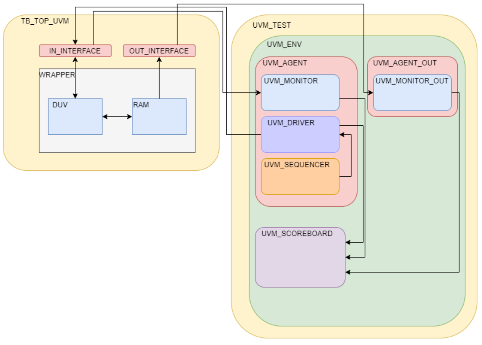
TB_TOP_UVM (Top Level Testbench)
This is the highest-level component in the UVM testbench hierarchy. It serves as the container for the entire UVM test environment, including the instantiation of the DUV, interfaces, and the UVM environment itself. The top level is responsible for initializing the test and setting the stage for the verification process.Interfaces (IN_INTERFACE, OUT_INTERFACE)
IN_INTERFACE: This interface module manages the inputs to the DUV. It defines the protocol and signal-level interactions that are fed into the DUV, ensuring that the DUV receives correct and timely test data. OUT_INTERFACE: Similar to the IN_INTERFACE but for outputs, this module captures and structures the outputs from the DUV, facilitating further analysis and verification against expected results.DUV (Design Under Verification)
This module is the actual target of the verification process. It represents the new or modified hardware design that needs to be rigorously tested to ensure it meets the specified requirements and behaves as expected under all operational conditions.RAM
This component models the memory elements that the DUV interacts with. It is crucial for tests that involve verifying the DUV’s behavior in scenarios that include data storage and retrieval, simulating real-world memory interactions.UVM_TEST
This component defines the specific test scenario to be run. It configures the UVM environment and other test parameters. Each UVM_TEST is typically tailored to verify different aspects of the DUV or to simulate different operational conditions.UVM_ENV (UVM Environment)
The UVM_ENV is a comprehensive container that holds various UVM components such as agents, monitors, and scoreboards. It is responsible for managing the interactions between these components and ensuring coherent operation throughout the test.UVM_AGENT
UVM agents are modular units that typically include a UVM driver, UVM sequencer, and UVM monitor. Each agent is focused on a specific part of the DUV interface or functionality, handling both the driving of test sequences into the DUV and monitoring the resulting behaviors.UVM_DRIVER
The driver takes sequence items from the sequencer and actively drives signals onto the bus or interface based on these items. It plays a direct role in how stimuli are applied to the DUV during testing.UVM_SEQUENCER
The sequencer generates the sequence items that dictate the actions to be performed by the driver. It controls the timing and order of these actions, which are crucial for the coherence and efficacy of tests.UVM_MONITOR
Monitors are observational components that watch the activity on the DUV’s interfaces without affecting the operation. They collect data necessary for analysis and for checking the results against expected behaviors.UVM_SCOREBOARD
The scoreboard compares the actual outputs from the DUV against the expected outputs to verify correctness. It is essential for determining the success or failure of the test scenarios and for identifying discrepancies.UVM_AGENT_OUT, UVM_MONITOR_OUT
These are likely additional monitoring and interfacing components designed to handle other specific outputs or secondary interfaces of the DUV. They ensure comprehensive coverage by monitoring all aspects of the DUV’s behavior.Test Plan
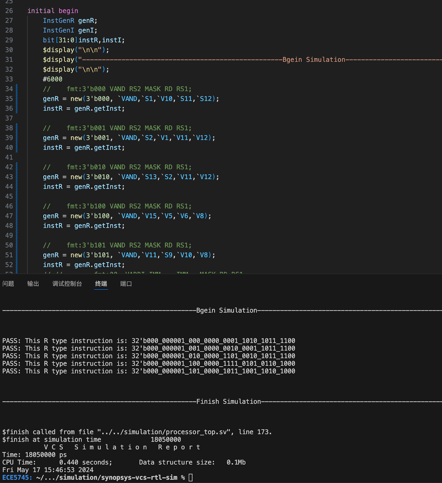
We also built an instruction generator in SystemVerilog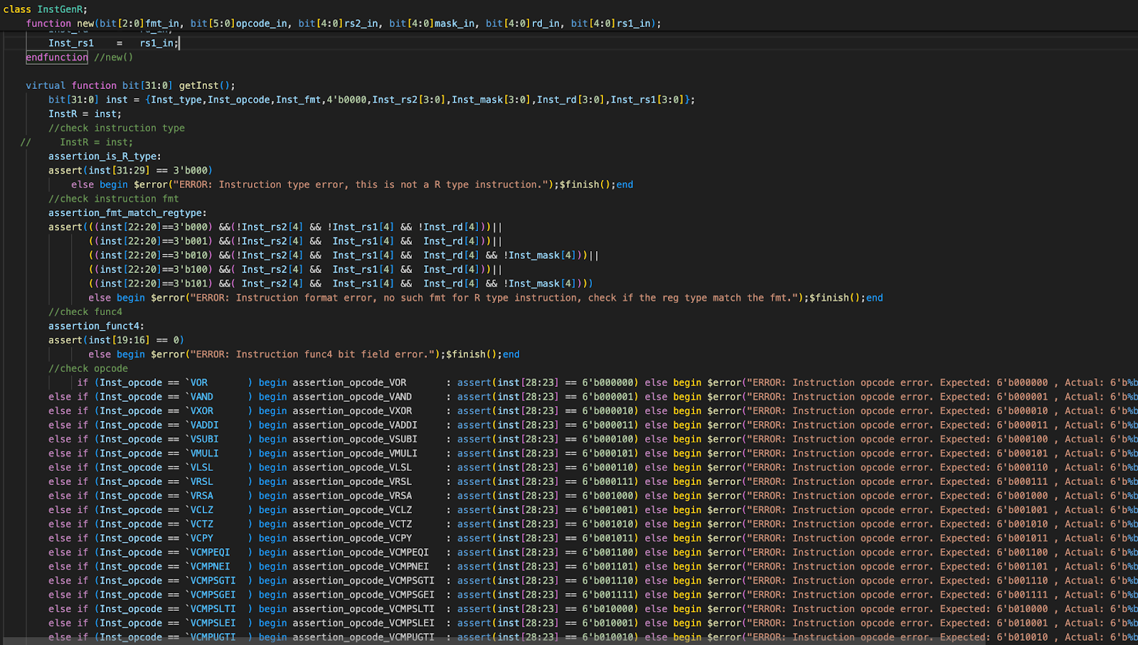 It can generate the instructions we want or in random constarint. For instance,
GPU
The GPU can be divided roughly into 4 sections.- Memory Management Unit
- VGA Controller
- GPU State Machine
- Render Pipeline
dma_req port to either request a read from SDRAM or write to SDRAM. Each port has a priority so that the VGA Controller would get the highest priority port while the other units could wait before their request is fulfilled.
The VGA Controller handles the job of reading from the color buffer and displaying the appropriate pixels onto the VGA screen. It contains the ports to read from the internal cache of 1024 pixels and make DMA requests with the MMU as well as the ports for a VGA signal
vga_signal. Internally it tracks which pixel is currently displayed, incremented by the signal from a modified version of the VGA driver provided in Lab2 which flags when it is inside the active zone.
Because of the memory arrangement described previously, each DMA request covers only 32 half words, corresponding to exactly one row of one tile. The local pixel cache acts as a buffer for when other modules need to perform DMA requests, so that the screen does not run out of pixels to show.
The GPU State Machine handles the more simple or miscellaneous tasks of the design. Crucially, here is where all commands are processed, like changing the stride of a vertex, changing the background color, or clearing the color or depth buffer. It also controls when to start and what parameters to feed into the render pipeline like the length and start of the vertex buffer.
Each command is a 32-bit long value passed in through a val rdy interface
| Command | Description | Bit Distribution |
|---|---|---|
| SWAP_BUFFER | Swaps which of the 2 frame buffers is the display and which is being rendered to. | 000_00000_00000000_00000000_00000001 |
| CLEAR_COLOR_BUFFER | Sets the color part of the render buffer to the background color. | 000_00000_00000000_00000000_00000010 |
| CLEAR_DEPTH_BUFFER | Sets the depth part of the render buffer to -1 depth. | 000_00000_00000000_00000000_00000011 |
| RENDER_BUFFER | Begin rendering based on vertex shader, vertex buffer ptr, and vertex buffer length. | 000_00000_00000000_00000000_00000100 |
| FLUSH_RENDER | Flush all cached color and depth buffer tiles in the render pipeline. | 000_00000_00000000_00000000_00000101 |
| SET_VERTEX_LENGTH | Sets how many floats represent 1 vertex. | 001_00000_00000000_00000000_0000???? |
| SET_BACKGROUND_COLOR | Sets the background color. | 010_00000_00000000_????????_???????? |
| PROGRAM_VERTEX_SHADER | Loads the vertex shander with data from the dual port SRAM starting at the address specified. | 011_00000_00000000_????????_???????? |
| PROGRAM_FRAGMENT_SHADER | [Currently Unused] | 100_00000_00000000_????????_???????? |
| SET_VERTEX_BUFFER_PTR | Sets the address to start fetching vertices from during a render operation. | 101_00000_????????_????????_???????? |
| SET_VERTEX_BUFFER_LENGTH | Sets the number of bytes to fetch during a render operation. | 110_00000_????????_????????_???????? |
| RENDER_DEBUG | Perform a debugging render operation using data from the on-chip ROM. | 111_11111_11111111_11111111_00000000 |
Render Pipeline
Vertex Fetcher
It starts by triggering the vertex fetching and feeding it the vertex buffer ptr and vertex buffer length from the GPU state machine. It collects every half word, truncates the last 5 bits, and pushes out afloat27 from dataport_27. The fetcher has no notion of what is a vertex, only what is a float, and will continue until it has gone through the entire buffer as defined by the ptr and length.
Vertex Shader
Here we perform transformations on the inputted vertex and is where the notion of a vertex is first acknowledged. From this point forward, all modules will have avertex_len port to accept an appropriate number of 27-bit wide data. 27-bits will also from here on be referred to as words, unlike the typical definition of 32-bits.
Our vertex shader is a hardcoded one which only performs a simple homogeneous matrix multiplication on the first 3 words of a vertex (with the assumption that they represent x,y,z). The "programming" performed in this context is simply loading the internal matrix of the vertex shader in a row major order from the SRAM.
The vertex shader first consumes 3 words treated as
float27s. It performs a homogeneous 4x4 matrix multiplication with a 4x1 vector consisting of the first 3 floats and 1. Then it renormalized the output vector by dividing by the last element of the resultant vector. To reduce stalling, the last element is actually computed first so the reciprocal can be computed in parallel to the other 3 elements. After the point has been transformed, it then pushes out the first 3 elements of the vector and consumes another vertex_len-3 words which are passed directly to the output.
Here the original plan was to utilize the SIMD processor to parallelize the vertex shading process as well as provide a high amount of customizability by allowing the user to write to the processor's instruction memory before each render operation.
Tiler
Here the module consumes3*vertex_len words and treat them as floats from the vertex shader and organize them into a triangle. Using the edge algorithm described above, starting at (-1,-1), it is able to compute the sidedness of each point. It computes and stores the sidedness of the lattice points, using a stride of 32 pixels, of each tile (21 x 16 points for 20 x 15 tiles) with respect to each side of the triangle independently. Then for each potential tile, we take the 4 lattice points of a line and if at least one of the 4 points is "inside" the line we treat the tile as being "inside" said line. If a tile is then "inside" of all three lines then we treat it as being "inside" said triangle and output the associated tile.
To do so, we feed the tile coordinates first into a fifo then to a submodule
gpu_tile_generator which has already stored the attributes of all 3 vertices. Upon receiving the tile coordinates from the fifo, it prepends the stream of words with 2 words dictating the minimum pixel xy and maximum pixel xy of the tile before streaming out the 3*vertex_len words representing the attributes of the triangle.
Rasterizer
First it consumes3*vertex_len+2 words where the first 2 words encode the tile information and the remaining 3*vertex_len are the triangle attributes. This time during the setup, instead of starting at (-1,-1), it starts at the minimum xy of the tile. It also precomputes the reciprocal of twice the total area of the triangle in anticipation of the interpolation. This time the iteration stops at the maximum xy of the tile while moving with a stride of 1 pixel as opposed to 32 pixels in the tiler. As each tile consists of 1024 pixels this process takes 1024 cycles after the initial setup. For each pixel which is "inside" the triangle, the coordinates get pushed into a fifo before getting fed into a submodule, interpolation unit, for interpolation.
This submodule computes the perspective corrected barycentric coordinates by multiplying sub triangle areas by the z coordinates of the base edge vertices before normalizing the three areas.
 The interpolation is then performed using the perspective corrected barycentric coordinates by doing multiply and reduction add in a pipeline. The interpolated z is used for depth testing by comparing to the value stored in the depth buffer cache. If the depth is farther than what is stored in the buffer the interpolation unit resets, awaiting for the next pixel to interpolate. If the depth is closer, the stored depth is overwritten and the interpolation unit continues interpolating the other attributes and outputs the pixel xy coordinates followed by the interpolated values for a total of
 vertex_len+1 words.
Fragment Shader
The fragment shader acceptsvertex_len words. This is also a hardcoded fragment shader which assumes the 4th, 5th, 6th attributes correspond to red, green, and blue of the pixel. The first word containing the x (10-bits) and y (10-bits) coordinates is converted into a address (10-bits) for the current tile it is processing It converts the float27 of RGB into a 16-bit color of 5-bits red, 6-bits green, and 5-bits blue. The address and color is combined into (26-bits) and output through a dataport_27 with a 0 pad as a single word.
Here the original plan was also to utilize the SIMD processor to parallelize the fragment shading process and provide a high amount of customizability by allowing the user to write to the processor's instruction memory before each render operation. A customizable processor would enable more complex rendering patterns like lighting or toon-shading without any hardware changes.
Raster Shading Pipeline
This is a module that wraps around the Rasterizer and Fragment Shader which checks the incoming tile and determines if the currently cached tile needs to be swapped out as well as accepting the output from the fragment shader and writing the color back to the cache.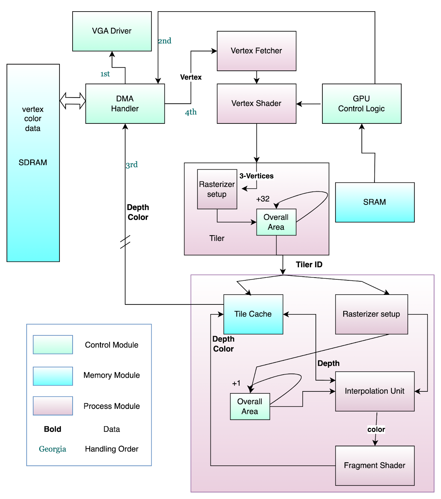
Design Choices/Changes
The structs likedataport_27 and vga_signal are just wrapper to make the input/output ports of our modules look cleaner. While the dma_signal is intended to act as a general port for DMA requests that is agnostic to the particular IP used to perform the DMA so that the RTL we write can be more simply fitted to the final design on the SoC.
Initially the rasterizer worked on a 18-bit fixed point arithmetic which provided sufficient resolution for triangles contained inside of the viewing frustum. However, when considering the necessary to clip triangles which extend past the view frustum it became apparent that using floating point arithmetic was far more straightforward where the cost of extra resource utilization is justified.
Results(To Top)
Rendering
We were unable to successfully deploy the design onto the SoC due to issues with the Intel DMA IP and not able to satisfy the memory requirements of our design. However, the simulations suggest that with a proper memory channel setup the deployment should be relatively smooth. Our simulation of the entire GPU consists of an emulated VGA device which accepts the outputvga_signal from the design and when triggered will also print to the console, the next available frame. With this we were able to simulate the renderings of a few sample images which are displayed at the top of this page.
The duration of the renderings range from ~20ms for the simpler shapes to ~300ms for the more complex shapes (utah teapot). From the images it would also seem that occasionally, some pixels would be missing or written to the wrong address. Our guess with why this occurs is poor synchronization between the many stages of our rendering pipeline resulting in occasional dropped pixels or late pixels.
Conclusion(To Top)
Although the design wasn't able to run on the SoC properly, the simulation was able to function mostly as intended with triangle rasterization. There are some minor glitches in the final rendering, likely due to errors in synchronizing, but the basic functionality of a triangle rasterizing, depth testing, vertex and fragment shading works as expected. To improve on the design for next time would likely involve another major refactoring of the entire code base. The goal would be to further modularize the design making it easier to make modifications and extensions, which was becoming increasingly difficult towards the end of this project. The other major change would be a major rework of the MMU, likely utilizing a common bus instead of parallel ports.Other optimizations to consider for any future works could be
- Using triangle bounding box to reduce tiler search space
- A more efficient raster scanning pattern which increments to the next row if the current row encounters a miss
- Tile binning to reduce memory bandwidth requirements
- Parallelize multiple interpolation units and fragment shaders
Appendix(To Top)
Course Page Inclusion
The group does approves this report for inclusion on the course website.Youtube Channel Inclusion
The group does not approve the video for inclusion on the course youtube channel.Verilog Code
Tasks
Yanwen Zhu (yz2949)
- SIMD Processor Pipeline
- UVM Framework
Rhoda Ma (rm2238)
- SIMD Processor ISA Testing
Bill Lui (sl2873)
- Entire Render Pipeline (without SIMD Processor)
- 27-bit Floating Point Processing Logic
Referneces
- Fast Inverse Square Root https://en.wikipedia.org/wiki/Fast_inverse_square_root
- Rasterization https://www.scratchapixel.com
- UCSD CSE 167 Computer Graphics https://cseweb.ucsd.edu/~tzli/cse167/fa2023/
- Juan Pineda. 1988. A parallel algorithm for polygon rasterization. SIGGRAPH Comput. Graph. 22, 4 (Aug. 1988), 17-20. https://doi.org/10.1145/378456.378457
- Embedded Peripherals IP User Guide https://www.altera.com/en_US/pdfs/literature/ug/ug_embedded_ip.pdf