My senior project is to design and build a digital
oscilloscope for Professor Land. This project involves a number of design
challenges. On the analog side, I need a fast, low noise A/D converter.
In addition, the circuit requires a -20V bias from a 5V supply. In the
realm of digital, it involves interfacing two micro-controllers with each
other, an LCD display, and an analog to digital converter. With such a
broad range of challenges, I searched for help from my professors and contacts
I made on the web. I was successful in getting help on floating point arithmetic
for an 8 bit micro-controller and LCD interfacing. I not only learned to
overcome technical challenges through design innovation and external resources,
but also worked with compromises between price, availability, and function.
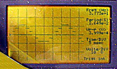
The above picture shows the display of the oscilloscope.
Notice that the wave form, a sign wave, is missing the lower four significant
bits. At the time the picture was taken, those bits on the A/D were
blown. Because most of the time the scope was in this state (the
A/D was VERY static sensitive) this picture is appropriate. The frequency
and period calculations are displayed on the right hand side of the display.
A quick hand calculation using the displayed time base demonstrates that
these calculations are correct. Unfortunately, at this time the voltage
scaling was not working, so it's displayed result has no meaning.
The goals of this project:
To demonstrate the capabilities of the ATMEL 8515 micro-controller
To learn about the difficulties in making something outside of the
shelter of a course
To have a practical, cheap digital oscilloscope
To build something cool
This oscilloscope implements the following functions:
Sections
Project Overview
Architecture
Processor to Processor Communication
Display Update Techniques and Communication with
LCD
LCD Memory Management
User Inputs
Floating Point Arithmetic
Trigger Modes
Voltage Scaling
Part Selection
LCD Displays
Power Supplies
Resources
Assembly Code
Parts list
Lab setup
Below are the connections for both micro-controllers, the LCD display, and the ADC.
Micro-controller 1:
PORT A (0..7): LCD data
PORT B (0..3): LCD control
PORT B (5..7): micro-controller 2 port D(5, 3, 7, 2)
PORT C (0..7): micro-controller 2 port C
PORT D (0..7): Buttons for user control
Micro-controller 2:
PORT A (0..7): A/D data
PORT B (0..7): Voltage scaling
PORT C (0..7): micro-controller 1 port C
PORT D (2..7): B7, B5, Ext. Trig., B4, A/D control, B4
The above figure shows the connections between the components of the oscilloscope. The arrows indicate the data direction.
The use of two micro-controllers allows distribution of the code and tasks at the expense of increased hardware and complexity. Micro-controller 1, the master, controls the LCD display, initiates communication with micro-controller 2, the slave, and takes in user information. In addition, it keeps track of the trigger mode and the time base. The slave deals with data acquisition from the A/D converter, voltage scaling, and performs the floating point arithmetic necessary to convert from pixels to voltages and times. The true necessity for two processors comes about because once the data acquisition starts, it can't be interrupted or the time base will not be accurate. During data acquisition, the user may want to make changes to the time base or trigger mode, so another processor must deal with the user interface. For example, if the time base is set very large, it might take 10 seconds to acquire the data. During this time, the LCD displays the previously acquired data. The user can make changes to the time base and trigger mode, and these changes will be displayed on the screen, but they will not take effect until the next data acquisition. For smaller time bases, this is not as much as a problem.
Additional advantages are gained with the use of two controllers. One of the main limiting factors for the Atmel 8515 micro-controller is limited ports. The use of two controllers allows more ports to simplify communication with the other devices. Also, having a separate controller allows the LCD refresh rate to be independent of the data acquisition rate.
The master controls the system processes. It sits in a loop, always updating the display, taking in user input, and asking the slave if it is ready to send data. With this technique the controller, not the time base, controls screen updates. When the slave finishes acquiring signal data, it calculates the Vp-p, frequency, and period, and then waits to be prompted for communication. When prompted, it sends the raw voltage data, the results of the floating point calculations, and then receives the time base and trigger mode for the next set of data. The master then displays the new data, takes user input, and checks for the slave to be ready again.
Due to the architecture of the communication between the two processors, many communication problems had to be resolved. Ports B(4..7) on the master and ports D(2,3,5,7) on the slave are used in communication between the two controllers. The block diagram above shows their connections and data directions. Port D7 on the slave indicates to the master when it is ready to start communication. When this pin is raised, the slave has completed acquiring the wave form and is ready to begin uploading data. Port B7 on the master synchronizes communication with the slave. When B7 is toggled, the slave puts data on Port C. The master assumes a fixed time delay, then reads the data off of Port C. When the data set and floating point numbers are finished uploading to the master, Port C changes direction, and the master uploads to the slave the new trigger conditions and time base.
The master uses port B5 to interrupt the slave in special trigger conditions. When the slave is in hold mode, it acquires one sample of data, sends it, and then sits in it's acquire data loop. However, because it's in a hold trigger condition, it does not acquire another sample. It would sit here infinitely because in this loop it can't communicate with the master to know if the trigger mode has changed. This interrupt sent of port B5, or pulse, resets the loop, allowing the slave to get a new set of data and communicate with the master. It is used whenever the trigger mode is changed, when the user requests to get a new sample in the hold mode, and when the user requests to upload data. Port B4 on the master tells the slave if it should enter the upload data state when the pulse is applied.
The LCD display has a built in T6963C display driver. It includes built in memory, the ability to display characters, and manages screen refresh and LCD control. Steve Lawther (bless his soul) rewrote the unreadable spec sheet on the T6963C into English. It clearly states how to send data and commands to the T6963C driver, and can be found in the references section.
The T6963C controller maintains two sets of memory, the graphics area and the text area. The graphics area is a direct bit mapping from memory to the LCD display. An on bit in the graphics area represents a dark pixel on the LCD. The text area also maps directly to the display, but instead of pixel by pixel mapping eight bits of memory maps to a character area (8x8) on the display. Additional features of the controller that I didn't use allow the user to create custom characters. The memory addressing is explained in further detail in the LCD control section.
Because there is a direct mapping between memory and what is displayed, as each byte is individually changed in memory, the change is directly seen on the display. Therefore erasing the LCD by consecutively erasing bytes is slow, and encourages flickering because the entire screen is not updated at once.
To minimize flickering and allow screen updates, the scope data is stored twice in the master controller. It stores the current data and the previous data. The master first erases the previous data, draws the new data, and then redraws the axis (in case they were erased when erasing the previous data). Finally it updates the statistics on the wave form. This technique greatly reduced the flickering until it was barely noticeable.
The T6963C controller for this LCD comes with approximately 8K of memory. It is divided into two user defined parts, one for graphics memory and one for character memory. It also has the option for user defined characters, but this feature is not utilized for this project. The graphics memory has a one to one relationship between set bits and on pixels. The character memory maps characters stored in an internal ROM to the corresponding location of the LCD.
The character width can be set to 8 bits or 6 bits. At 6 bits, characters are only 6 bits wide. However, the 6 bit setting uses significantly more memory because this also affects the graphics memory. On the 6 bit setting, only the lower 6 bits are significant because each graphics block is considered to be six bits long. Since my main concern was fitting as much data as possible on the screen, I chose the 6 bit option because it allows characters to take up less space.
The graphics memory is set to start at 0000h. For
a 240 x 128 display, the number of bytes required to represent a single
line across the screen in 6 bit mode is 240 / 6 = 40. Multiplying this
by 128 lines results in 5120 bytes required for graphics memory. Therefore
the character memory must start after this at 1400h. The character memory
requires 40 bytes per 8 bit high line, resulting in a memory usage of 320
bytes. The total memory usage is 5440 bytes, which is well below the 8K
memory maximum.
|
|
|
|
|
|
|
|
|
|
|
|
|
|
|
|
|
|
|
|
| 1658h |
|
To write the data to memory it is necessary to transform the data format. The initial data format is a series of 128 bit numbers, each of which represents a voltage. This must be transformed to a format where it can be written to memory. The following structure performs the transformation:
For mempointer = 13D8h to 167Fh
*loop across bottom of graphics memory
Mempointertmp = mempointer
*setup temporary variable
Voltage = memory(Z+)
*get value to display
For bit = 0 to 5
*loop across 6 bits for each memory location
For cnt =
0 to voltage
Mempointertmp += -40
*shift pointer up one row for each voltage tick
Next cnt
Write bit
to Mempointertmp
*write bit to position at Mempointer
Next bit
*ie: write 0th through 5th bits because each address has six bits
Next mempointer
This routine writes/erases the wave form data from memory to the LCD
display.
The user input for the oscilloscope consists of eight debounced buttons:
7: Increase Trigger Level
6: Decrease Trigger Level
5: Increase Time base
4: Decrease Time base
3: Toggle Grid on/off
2: Set Trigger Mode
1: In a hold trigger mode, acquire a new sample of data
0: Start data upload
The user input presented an interesting concurrency problem. Timer 0 interrupts and scans the input keys. It then runs through a quick debounce routine and determines what button was pressed. If a button was pressed, it sets a flag. This results in the quickest possible interrupt because it does not actually do anything with the change, just acknowledge that a button was pressed. It is necessary to keep this interrupt short because I found that if a long interrupt occurs during communication with the LCD, the delay can blank out the LCD display. This problem is minimized by shortening the interrupt and making it less frequent. Another possible solution is turning off the interrupt when communication with the LCD occurs. Unfortunately, this results in missed keyboard scans, so the processor could miss a key press.
One of the original goals of this project was to implement 32 bit floating point arithmetic on the 8 bit micro-controller. The thought of writing the code myself was a little daunting, so I looked on the web for support. Atmel's application notes don't cover FP, but I was able to find code by Jack Tidwell that implemented 32 bit floating point arithmetic. It was fairly straight forward to implement his code into the oscilloscope, and whenever I had problems he was very prompt and helpful in his responses. He even spent a couple of hours working on a section that I needed for my project. His routines are in the assembly code section, and his web page is in the resources section. To calculate Vp-p, the slave micro-controller determines the maximum and minimum of the signal. Next it multiplies the difference by a voltage factor that is a function of the Vp-p scaling. To determine period and frequency, it looks for the input signal to cross the trigger level twice with a positive slope. The scope outputs an error signal for period and frequency if the input is not triggered.
The oscilloscope supports four data acquisition modes:
1: Internal
The internal trigger triggers on the rising edge of a trigger level
set by the user, indicated by an arrow on the left of the display. When
a trigger condition is not met after 250 data points, the signal is displayed
without the trigger, resulting in a moving wave as seen on Tektronix oscilloscopes
when the trigger condition is not met.
2: Internal Hold
The internal hold waits until the trigger condition is met. When it
is met, the scope will acquire one set of data and displays it. The scope
does not acquire another set of data, allowing the user to view a non periodic
event.
3: External
The External trigger takes an external digital input and triggers on
the rising edge of the external signal.
4: External Hold
The External Hold trigger is similar to the External trigger, except
it takes only one set of data and displays it, allowing the user to view
a single event.
Both hold modes offer an additional benefit. When data has been acquired in hold mode, the user has the option to upload the raw data from the slave processor to a PC. To accomplish this, the user presses the upload to PC button, and then executes a C program that acquires the data and stores it in text format. At this point, the data is stored as 256 bit numbers. Ideally, the processor would also send information about the time and voltage bases, allowing a program to completely reproduce the wave form. However, in the given time frame I was unable to implement this feature.
To keep things simple, the voltage scaling was ultimately implemented with resistor dividers and a double pole, eight position switch. One pole is used to switch the input signal through the correct resistor network, and the other pole is used to tell the slave micro-controller, through a one hot signal, which voltage scaling is selected. The processor can use this information to calculate the Vp-p value.
I had to choose three main parts for this project: the LCD display, negative voltage supply, and A/D converter. I designed around low cost, part availability, and functionality. Due to the short time frame of this project, approximately three months, shipping times for parts was of utmost importance. I quickly discovered MAXIM provides free samples of most parts, including DIP packages, good customer service, and quick shipping times. Consequently, the negative power supply and A/D converter are both MAXIM parts. The LCD display was significantly more difficult to find. For most companies, the selection and stock was poor because they manufacture for a specific order, resulting in large minimum orders and low availability. I finally decided on an LCD display because it was the only one I could find that met my size and controller requirements and was reasonably priced.
I started this project knowing nothing about LCD displays. Most web pages I encountered about LCD displays assumed some prior knowledge, and I had difficulty learning the basics. Hopefully this will give an overview of what to look for in LCD displays.
Controllers
The most important consideration in choosing an
LCD display is the controller. An LCD display without a controller needs
to be refreshed at a fast enough rate to prevent flickering. This would
have been almost impossible using the ATMEL 8515 due to memory and speed
restrictions. Therefore I looked into getting a display with a built in
controller. The most popular, though slightly outdated standard is the
T6963C controller made by Toshiba. Another popular choice is the SED series
made by Epson. I chose the T6963C controller because it seemed relatively
easy to use and was offered in the display that I wanted.
Size
LCD graphics displays come in a variety of sizes,
ranging from 32 x 80 to 240 x 320. Larger displays offer more display area,
cost more, and take longer to refresh the entire screen with new data.
I chose a 128 x 240 display, giving myself enough space to show a 128 bit
wave form while leaving room on the side to display measurement values.
The following options are available on most LCD displays:
Display Type
There are three basic display types, TN, STN, and
FSTN. Twisted Nematic (TN) is the least expensive and most basic display
type. Super Twisted Nematic (STN) offers higher contrast, wider viewing
angles, and is available with different background colors. Film STN (FSTN)
is a black and white STN with a very high contrast ratio for large graphic
panels. Most graphic LCD displays manufactured today are STN.
Backlight
Backlights also come in three basic varieties, EL,
LED, and CCFL. Electro-luminescent (EL) is power efficient, but requires
an inverter to operate. Light emitting diode (LED) offers even back lighting,
long life expectancy (>100,000 hrs), is simple to drive with 5 volts, and
its brightness can easily be adjusted. Cold cathode florescent light (CCFL)
is paper white and consumes less power than LED, but it also requires an
inverter as a power supply. I was not concerned about back lighting, but
the display I chose came with LED, which is the easiest to operate. LED
backlights can be operated at a higher efficiency by driving them with
a pulse width modulated wave form.
Viewing Angle
The two basic viewing angles are defined as 12:00
and 6:00. A 12:00 display is best viewed below eye level, and a 6:00 display
is best viewed above eye level. I chose a 6:00 viewing angle to view a
flat screen on a desk.
Other issues
Choosing an LCD display is one of the easiest parts
of actually buying an LCD display. The most difficult part is finding a
company willing to sell and ship a single LCD display. Most manufacturers
don't want to deal with customers, and their sales reps will not waste
their time with single shipments. By the time I found someone willing to
sell me a single display, I was happy on settling with getting the desired
size and controller, and accepting any other options it came with. Because
of the difficulty in obtaining single quotes and my time constraints, I
was unable to systematically compare the prices of displays across different
companies and for different features.
What I bought
I ended up buying the ITM240128A graphics LCD display
from Micro Electronics Corporation for $85. It features a 6:00 viewing
angle, T6963C controller, a 240 x 128 pixel screen, STN, extended temperature,
and an LED backlight. The LCD display was well constructed, and survived
all of my mistakes when prototyping.

The micro-controller requires a 5V power supply to operate. This is easily obtained with a linear power supply that can be purchased at Radio Shack and a voltage supply anywhere from 7V to 20V (batteries). For this project I used a lab supply connected to a simple linear regulator.
The LCD display has more challenging power supply requirements. The display requires a low current (5.4mA) -20V bias. Originally, this was supplied using a lab supply. However, in the attempt to make this scope transportable, I found a switching supply that works off 5V and generates -20V. I decided on the MAX749. This part was readily available in an 8 pin DIP package, and is designed for just this purpose. The circuit, depicted above, worked as expected.
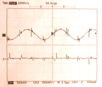
As with all switching power supplies, it added high frequency noise to the system. The switching currents added spikes on the power supplies, which consequently showed up everywhere in the system. The scope plot above shows the effects of the switching power supply on the GND of the system and a sine wave being fed through a unity gain op-amp. Spikes of almost 500mv are observed when the power supply switches. The addition of by-pass capacitors had little effect in reducing these spikes. There are many possible solutions, but with the given time frame I was unable to implement them.
1: Implementing a low impedance power supply would help reduce the spikes on the power rails
2: An A/D converter with an analog and digital ground could be used. The switching supply, LCD, and micro-controllers would use the digital ground, which would have the switching supply noise on it. The analog side of the A/D would be isolated from this noise, and could acquire noise free data. However, the entire system shares the same VDD, which still has noise on it.
3: The best solution is to isolate the two systems with an optical isolator. The noisy system consists of the switching supply, LCD display and micro-controllers. The clean system, running on a different power supply, consists of the A/D converter and any required level shifters.
These solutions provide practical methods to implement the oscilloscope with a single positive power supply. The negative bias voltage could also be generated with batteries.
This web page presents a large list of LCD manufacturers. This is all
you need to get started.
http://www.eio.com/lcdmanuf.htm
This page provides an assortment of useful info on LCD displays
http://www.citilink.com/~jsampson/lcdindex.htm
This is the original data sheet for the T6963C. It is very difficult
to understand, but makes a good reference.
Toshiba T6963C
If you actually want to use the T6963C controller in an LCD display
that comes with it (you dont attempt to wire it up to the display and
memory yourself) then all you need is the re-written data sheet at
T6963rr.pdf
This is very easy to follow, courtesy of Steve Lawther.
Specs for the MAXIM MAX749 negative voltage power supply
Power supply specs
Specs for the MAXIM MX7821 A/D converter
A/D converter
I would like to give special thanks to Jack Tidwell for his help with
floating point routines. His web page provides useful information
for Atmel micro-controllers and assembly compilers.
http://www3.igalaxy.net/~jackt/
Assembly Code
Master micro-controller code:
Master.txt
Slave micro-controller code:
Slave.txt
Floating point routines:
Fprout.txt
Macros for communication with LCD:
Macros.txt
Parts list
2 Atmel 8515 Micro-controllers
1 Maxim MAX749 LCD bias supply
1 Maxim MX7821 ADC
1 ITM240128A graphics LCD display from Micro Electronics Corporation
Lab Setup
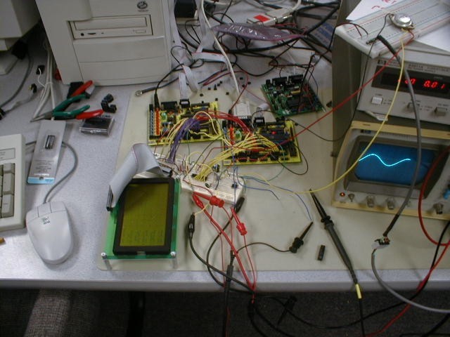
This is a setup of the proto-type oscilloscope. I used ribbon
cable and a breadboard to wire the LCD display to the micro-controllers.
Also visible on the breadboard, connected with yellow wires, is the analog
to digital converter. A function generator, oscilloscope, and lab
power supply completes the equipment required for this project.