
Figure 1 - Schematic of the state machine of SuperProcessor
2.1. The Fetch state:
2.1.1. The M4K module:
The M4K memory modules generated by Quartus Megawizard tool can be set to read-and-write or to read-only, and can either have one or two ports. On our implementation, the program memory is set to read-only for protection and has a single port. The data memory is set to read-and-write and has two ports, in order to increase the parallelism of the system.
2.2. The Execute state:
In this state, the current instruction completes its execution and the memory address register of program memory is updated with the content of the program counter or some other address if there is branching, so that the next instruction word is available in the following Fetch state.2.3. The MachineReset special state:
3. The Architecture
3.1. I/O Structure
Treating the SuperProcessor as a black box, we identify seven inputs and five outputs that compose the interface of this module with the prototyping board. These are depicted on figure 2.
Figure 2 - I/O schematic for SuperProcessor
Clock: the clock signal of SuperProcessor, which changes the state of its state machine after its negative edge. In order to have the proper synchronization between SuperProcessor and the audio codec for audio processing functions, it was necessary to have the clock signals of these two modules coming from the same crystal on the prototyping board. Therefore, Clock is generated on the same phase-lock-loop of CLOCK_27(the audio codec clock signal).
Reset: the reset signal of SuperProcessor, which leads its state machine to the MachineReset state.
StereoInputRight: audio input to the processor from the prototyping board corresponding to the right stereo channel.
StereoInputLeft: audio input to the processor from the prototyping board corresponding to the left stereo channel.
SwitchInput: input to the processor from the switches of the prototyping board.
KeyInput: input to the processor from the keys of the prototyping board.
StereoOutputRight: audio output from the processor to the prototyping board corresponding to the right stereo channel.
StereoOutputLeft: audio output from the processor to the prototyping board corresponding to the left stereo channel.
HexadecimalOutput: output from the processor to the 8 digits of the 7-segments display on the prototyping board.
LEDOutput: output from the processor to the red leds on the prototyping board.
SincLR: the audio codec clock, used for synchronization.
PIN0: output for debugging – it maps the GPIO pins of the prototyping board.
3.2. Translation of the instruction word:
The translation of the instruction word occurs on the following steps:1) First of all, the content of the program counter is transferred to the address register of program memory (for an explanation of how the program memory works, refer to section 1.1.1). It occurs on the Execute cycle of each instruction, in order to have the instruction word of the next instruction available by the beginning of the next cycle (a Fetch cycle). This first step is different in some instructions, refer to section 5 for details.
2) As soon as the program memory makes available the instruction word corresponding to the given address, combinational logic divides the instruction word into the following elements: bits 31 to 26 are the opcode, bits 25 to 21 are operand code 1 (used to select operand register 1), bits 20 to 16 are operand code 2 (used to select operand register 2) and bits 15 to 0 are the immediate operand.
3) Still using combinational logic, operand code 1 is input to a multiplexer. This multiplexer selects which one of the registers of the machine will be operand register 1. The same occurs to operand code 2.
This architecture is summarized in Figure 3.
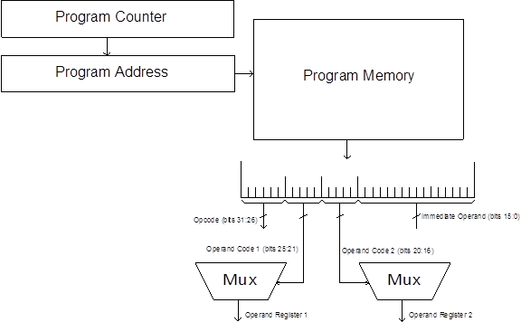
Figure 3 - Architecture for the translation of the instruction word
3.2.1. Exceptions on step 1:
In branching instructions, the first step on the translation of the instruction word consists in updating the content of the address register of program memory, but not necessarily with the content of the program counter. Instead, the content of the address register of program memory can be updated with the content of operand register 1 or with the value of the immediate operand.3.3. Data memory interface:
The data memory is dual-port and configured for reading and writing (for more details, refer to section 5). For most of SuperProcessor’s instructions, its interface with the machine – the address registers, reading registers and reading wires – is configured on a default way. This default way consists in: operand register 1 can get connected to the address register of port A, the immediate operand can get connected to the address register of port B, and operand register 2 can get connected to writing registers and reading wires of both ports. This architecture is summarized on Figure 4.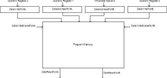
Figure 4 - Architecture of the data memory interface
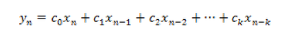
4. MAC:
The most important instruction for the audio processing application and the basis of convolution, the MAC instruction consists of a Multiplication followed by an addition. It uses all the time resources of the machine. For details on the implementation, refer to the instruction manual. The additional architecture needed consists of a combinational multiplication module, generated by Quartus MegaFunction tool, a special Accumulator and two hardware lists.To implement audio processing tasks we use the MAC instruction to implement the following equation for a filter of order k:
4.1. Accumulator:
The Accumulator is a special register used by the MAC instruction. It has 40 bits and its content is shown on Figure 5.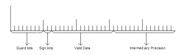
Figure 5 - Accumulator's structure
4.2. Hardware list:
To satisfy the timing requirements, we had to implement two hardware lists that update their pointers in hardware. A diagram that shows the behavior of the coefficient list is on Figure 6.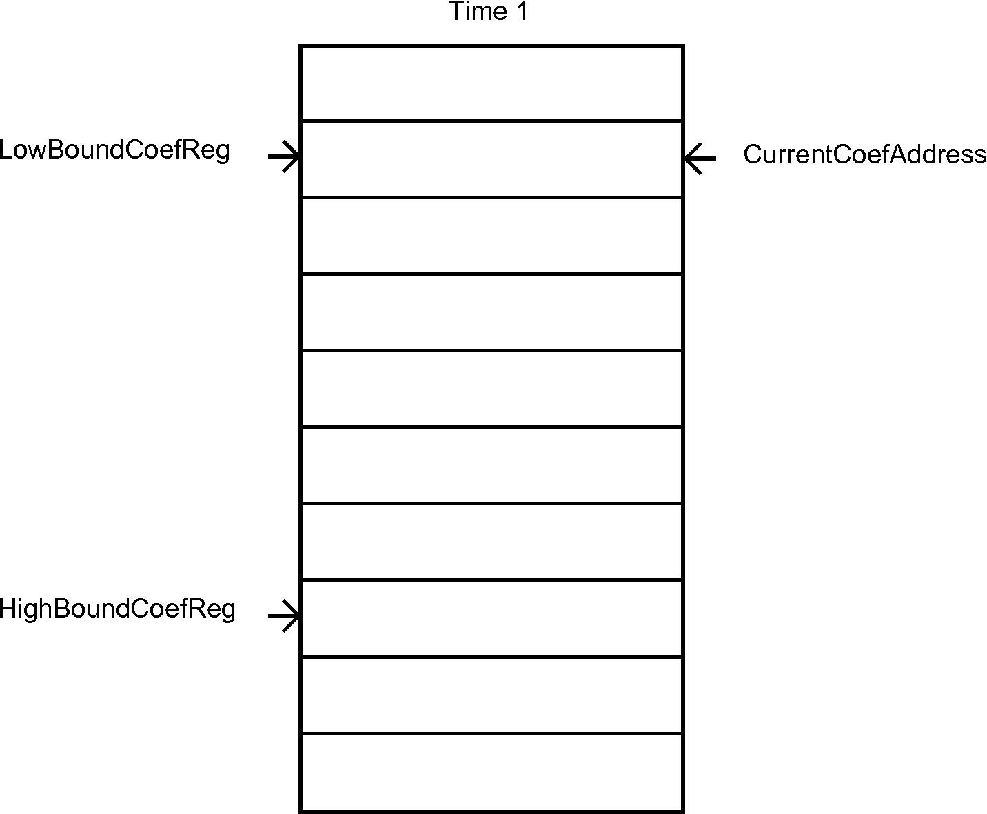
Figure 6 - Hardware list for the coefficients
The next list, the one that handles the Data Samples, is a bit more complicated. Figure 7 is an animation that give the sense behind its behavior.
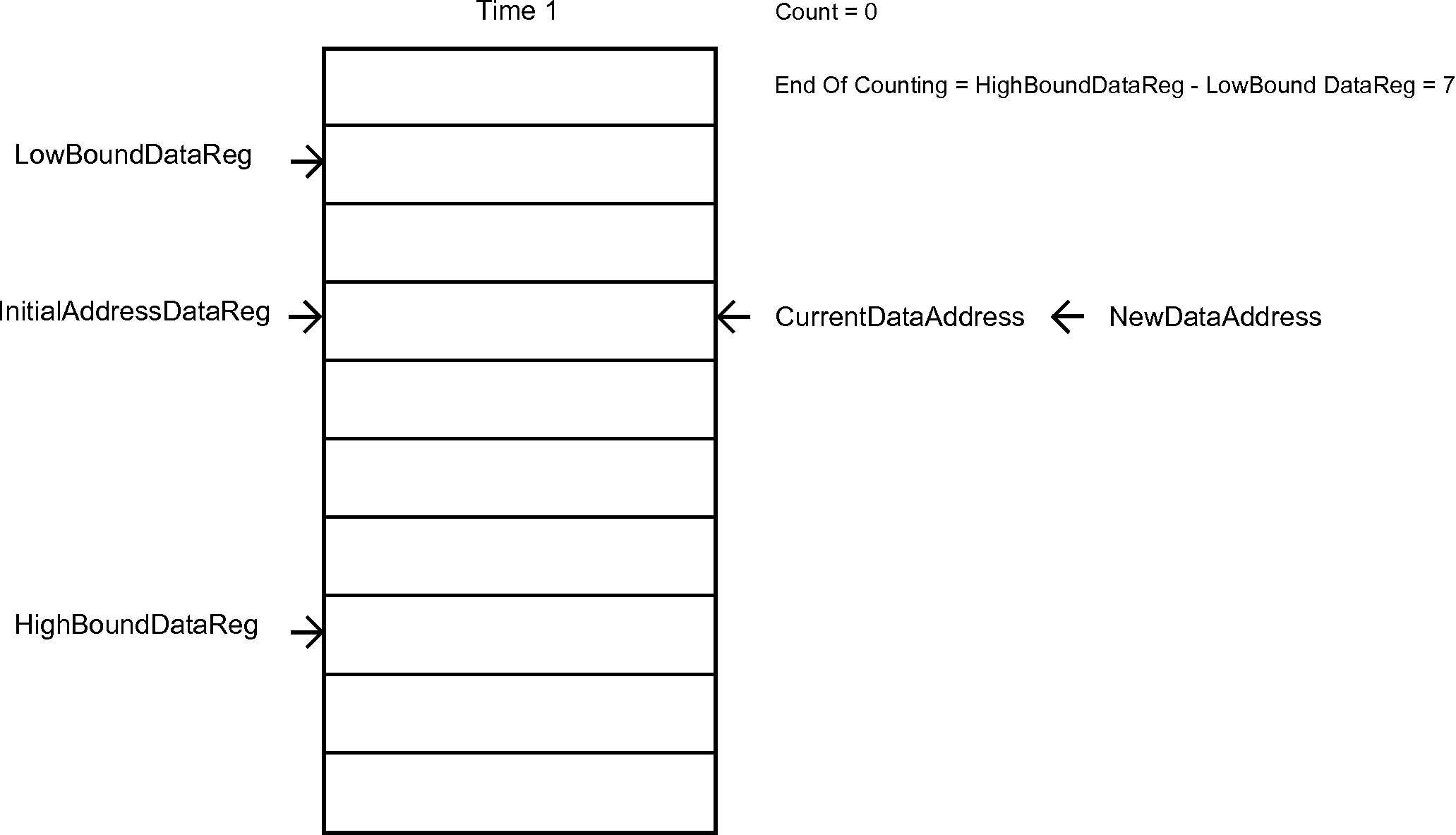
Figure 7 - Hardware List for the data samples
5. The instruction set:
The instructions are listed according to the sequence of opcodesExplanations about the particular use of port A or port B of data memory are found on the architecture section.
5.1. Arithmetical instructions:
5.1.1. ADD:
Opcode: 0Syntax: ADD R1, R2;
Description: adds the contents of two registers and stores the result on the first register specified.
R1 <= R1 + R2;
Implementation:
OperandRegister1 <= OperandRegister1 + OperandRegister2;
ResultRegister <= OperandRegister1 + OperandRegister2;
5.1.2. ADDI:
Opcode: 1Syntax: ADD R1, value;
Description: adds the content of a register to the value of an immediate operand – which can be a decimal number or a label.
R1 <= R1 + value;
Implementation:
OperandRegister1 <= OperandRegister1 + ImmediateOperand;
ResultRegister <= OperandRegister1 + ImmediateOperand;
5.1.3. INC:
Opcode: 2Syntax: INC R1;
Description: increments (adds the decimal 1) the content of a register.
R1 <= R1 + 1;
Implementation:
OperandRegister1 <= OperandRegister1 + 1;
ResultRegister <= OperandRegister1 + 1;
5.1.4. SUB:
Opcode: 3Syntax: SUB R1, R2;
Description: subtracts the content of the second register specified from the content of the first register specified and stores the result on the first register specified.
R1 <= R1 - R2;
Implementation:
OperandRegister1 <= OperandRegister1 - OperandRegister2;
ResultRegister <= OperandRegister1 - OperandRegister2;
5.1.5. SUBI:
Opcode: 4Syntax: SUBI R1, value;
Description: subtracts the value of an immediate operand – which can be a decimal number or a label – from the content of a register and stores the result on this register.
R1 <= R1 - value;
Implementation:
OperandRegister1 <= OperandRegister1 - ImmediateOperand;
ResultRegister <= OperandRegister1 - ImmediateOperand;
5.1.6. DEC:
Opcode: 5Syntax: DEC R1;
Description: decrements (subtracts the decimal 1) the content of a register.
R1 <= R1 - 1;
Implementation:
OperandRegister1 <= OperandRegister1 - 1;
ResultRegister <= OperandRegister1 - 1;
5.1.7. LSFT:
Opcode: 6Syntax: LSFT R1, R2;
Description: shifts to the left the bits of the content of R1 by a number of positions which corresponds to the content of R2, being R1 and R2 the first and the second registers specified respectively.
R1 <= R1 << R2;
Implementation:
OperandRegister1 <= OperandRegister1 << OperandRegister2;
ResultRegister <= OperandRegister1 << OperandRegister2;
5.1.8. LSFI:
Opcode: 7Syntax: LSFI R1, value;
Description: shifts to the left the bits of the content of a register by a number of positions corresponding to the value of an immediate operand – which can be a decimal number or a label.
R1 <= R1 << value;
Implementation:
OperandRegister1 <= OperandRegister1 << ImmediateOperand;
ResultRegister <= OperandRegister1 << ImmediateOperand;
5.1.9. RSFT:
Opcode: 8Syntax: RSFT R1, R2;
Description: shifts to the right the bits of the content of R1 by a number of positions which corresponds to the content of R2, being R1 and R2 the first and the second registers specified respectively.
R1 <= R1 >> R2;
Implementation:
OperandRegister1 <= OperandRegister1 >> OperandRegister2;
ResultRegister <= OperandRegister1 >> OperandRegister2;
5.1.10. RSFI:
Opcode: 9Syntax: RSFI R1, value;
Description: shifts to the right the bits of the content of a register by a number of positions corresponding to the value of an immediate operand – which can be a decimal number or a label.
R1 <= R1 >> ImmediateOperand;
Implementation:
OperandRegister1 <= OperandRegister1 >> value;
ResultRegister <= OperandRegister1 >> value;
5.2. Logical operations:
5.2.1. NOT:
Opcode: 10Syntax: NOT R1;
Description: performs a bitwise NOT operation on the content of a register and stores the result on this register.
R1 <= NOT R1;
Implementation:
OperandRegister1 <= ~OperandRegister1;
5.2.2. AND:
Opcode: 11Syntax: AND R1, R2;
Description: performs a bitwise AND operation between the contents of two registers and stores the result on the first register specified.
R1 <= R1 AND R2;
Implementation:
OperandRegister1 <= OperandRegister1 & OperandRegister2;
5.2.3. OR:
Opcode: 12Syntax: OR R1, R2;
Description: performs a bitwise OR operation between the contents of two registers and stores the result on the first register specified.
R1 <= R1 OR R2;
Implementation:
OperandRegister1 <= OperandRegister1 | OperandRegister2;
5.2.4 XOR:
Opcode: 13Syntax: XOR R1, R2;
Description: performs a bitwise XOR operation between the contents of two registers and stores the result on the first register specified.
R1 <= R1 XOR R2;
Implementation:
OperandRegister1 <= OperandRegister1 ^ OperandRegister2;
5.3. Data moving operations:
5.3.1. LD:
Opcode: 14Syntax: LD R1, value;
Description: loads on a register the content of a data memory position adressed by the value of an immediate operand – which can be a decimal number or a label.
R1 <= (value);
Implementation: due to the behavior of the Altera M4K module, used to build both the data and program memories and explained on section 2.1.1, this instruction is executed in two cycles. So, we have the following implementation:
1st cycle (Fetch Cycle): DataAddressPortB <= ImmediateOperand;
2nd cycle (Execute Cycle): OperandRegister2 <= DataReadPortB;
5.3.2. LDI:
Opcode: 15Syntax: LDI R1, value;
Description: loads on a register the value of an immediate operand – which can be a decimal number or a label.
R1 <= value;
Implementation: OperandRegister2 <= ImmediateOperand;
5.3.3. LDIN:
Opcode: 16Syntax: LDIN R1, R2;
Description: loads on the second register specified the content of a data memory position adressed by the content of the first register specified.
R2 <= (R1);
Implementation: due to the behavior of the Altera M4K module, used to build both the data and program memories and explained on section 2.1.1, this instruction is executed in two cycles. So, we have the following implementation:
1st cycle (Fetch Cycle): DataAddressPortA <= OperandRegister1;
2nd cycle (Execute Cycle): OperandRegister2 <= DataReadPortA;
5.3.4. ST:
Opcode: 17Syntax: ST R1, value;
Description: stores the content of a register on a data memory position adressed by the value of an immediate operand – which can be a decimal number or a label.
value <= R1;
Implementation: due to the behavior of the Altera M4K module, used to build both the data and program memories and explained on section 2.1.1, this instruction is executed in two cycles. So, we have the following implementation:
1st cycle (Fetch Cycle): DataAddressPortB <= ImmediateOperand;
DataWritePortB <= OperandRegister2;
2nd cycle (Execute Cycle): DataWriteEnablePortB <= 1’d1;
5.3.5. STIN:
Opcode: 18Syntax: STIN R1, R2;
Description: stores the content of the second register specified on a data memory position adressed by the content of the first register specified.
(R1) <= R2;
Implementation: due to the behavior of the Altera M4K module, used to build both the data and program memories and explained on section 2.1.1, this instruction is executed in two cycles. So, we have the following implementation:
1st cycle (Fetch Cycle): DataAddressPortA <= OperandRegister1;
DataWritePortA <= OperandRegister2;
2nd cycle (Execute Cycle): DataWriteEnablePortA <= 1’d1;
5.3.6. MOV:
Opcode: 19Syntax: MOV R1, R2;
Description: “moves” the content of the second register specified into the first register specified (i.e., copies the content of the second register specified to the first register specified).
R1 <= R2;
Implementation: OperandRegister1 <= OperandRegister2;
Interface operations:
5.3.7. IN:
Opcode: 20;Syntax: IN R1, R2;
Description: copies the content of the second register specified, which is a registered input of SuperProcessor’s interface with the prototyping board, to the first register specified. This instruction is used for inputting data to the machine.
R1 <= R2;
Implementation: OperandRegister1 <= OperandRegister2;
5.3.8. OUT:
Opcode: 21Syntax: OUT R1, R2;
Description: copies the content of the second register specified to the first register specified, which is a registered output of SuperProcessor’s interface with the prototyping board. This instruction is used for outputting data from the machine.
R1 <= R2;
Implementation: OperandRegister1 <= OperandRegister2;
5.4. Branching instructions:
5.4.1. CMP:
Opcode: 22Syntax: CMP R1, R2, value;
Description: if two specified registers have identical contents, the program counter is set to a value given by an immediate operand – which can be a decimal number or a label. Otherwise, the program counter is incremented as usual.
if (R1 == R2)
PC <= value;
else
PC <= PC + 1;
Implementation:
ProgramAddress <= (OperandRegister1[15:0]==OperandRegister2[15:0])? ImmediateOperand[11:0] : ProgramCounter;
ProgramCounter <= (OperandRegister1[15:0]==OperandRegister2[15:0])? ImmediateOperand[11:0] : ProgramCounter;
5.4.2. BPL:
Opcode: 23Syntax: BPL R1;
Description: if the result of the last arithmetic operation executed on the program is positive, the program counter is set to a value which is stored on a specified register. Otherwise, the program counter is incremented as usual.
if (ResultRegister > 0)
PC <= R1;
else
PC <= PC + 1;
Implementation:
ProgramAddress <= (ResultRegister[15]==1'b0)? OperandRegister1[11:0] : ProgramCounter;
ProgramCounter <= (ResultRegister[15]==1'b0)? OperandRegister1[11:0] : ProgramCounter;
5.4.3. BPLI:
Opcode: 24Syntax: BPLI value;
Description: if the result of the last arithmetic operation executed on the program is positive, the program counter is set to a value given by an immediate operand – which can be a decimal number or a label. Otherwise, the program counter is incremented as usual.
if (ResultRegister > 0)
PC <= value;
else
PC <= PC + 1;
Implementation:
ProgramAddress <= (ResultRegister[15]==1'b0)? ImmediateOperand[11:0] : ProgramCounter;
ProgramCounter <= (ResultRegister[15]==1'b0)? ImmediateOperand[11:0] : ProgramCounter;
5.4.4. BMI:
Opcode: 25Syntax: BMI R1;
Description: if the result of the last arithmetic operation executed on the program is negative, the program counter is set to a value which is stored on a specified register. Otherwise, the program counter is incremented as usual.
if (ResultRegister < 0)
PC <= R1;
else
PC <= PC + 1;
Implementation:
ProgramAddress <= (ResultRegister[15]==1'b1)? OperandRegister1[11:0] : ProgramCounter;
ProgramCounter <= (ResultRegister[15]==1'b1)? OperandRegister1[11:0] : ProgramCounter;
5.4.5. BMII:
Opcode: 26Syntax: BMII value;
Description: if the result of the last arithmetic operation executed on the program is negative, the program counter is set to a value given by an immediate operand – which can be a decimal number or a label. Otherwise, the program counter is incremented as usual.
if (ResultRegister < 0)
PC <= value;
else
PC <= PC + 1;
Implementation:
ProgramAddress <= (ResultRegister[15]==1'b1)? ImmediateOperand[11:0] : ProgramCounter;
ProgramCounter <= (ResultRegister[15]==1'b1)? ImmediateOperand[11:0] : ProgramCounter;
5.4.6. JMP:
Opcode: 27Syntax: JMP R1;
Description: sets the program counter to a value contained on a specified register.
PC <= R1;
Implementation:
ProgramAddress <= OperandRegister1[11:0];
ProgramCounter <= OperandRegister1[11:0];
5.4.7. JMPI:
Opcode: 28Syntax: JMPI VALUE;
Description: sets the program counter to a value given by an immediate operand – which can be a decimal number or a label.
PC <= value;
Implementation:
ProgramAddress <= ImmediateOperand[11:0];
ProgramCounter <= ImmediateOperand[11:0];
5.4.8. JMPL:
Opcode: 29Syntax: JMPL R1;
Description: saves the current content of the program counter on a special register (ReturnRegister) and then sets the program counter to a value contained on a specified register. If the instruction RET is executed somewhere after the JMPL instruction, the old program counter content stored on the special register is reloaded into the program counter register. Due to concurrency on the manipulation of the program counter register, this instruction needs two cycles to be executed. On the first cycle, the content of the program counter is stored on a special register. On the second cycle, the program counter is set to a value contained on a specified register.
1st cycle: ReturnRegister <= PC;
2nd cycle: PC <= R1;
Implementation:
1st cycle (Fetch Cycle): ReturnRegister[11:0] <= ProgramCounter+12'd1;
2nd cycle (Execute Cycle): ProgramAddress <= OperandRegister1[11:0];
ProgramCounter <= OperandRegister1[11:0];
5.4.9. JMPLI:
Opcode: 30Syntax: JMPLI value;
Description: saves the current content of the program counter on a special register and then sets the program counter to a value given by an immediate operand – which can be a decimal number or a label. If the instruction RET is executed somewhere after the JMPL instruction, the old program counter content stored on the special register is reloaded into the program counter register. Due to concurrency on the manipulation of the program counter register, this instruction needs two cycles to be executed. On the first cycle, the content of the program counter is stored on a special register. On the second cycle, the program counter is set to a value given by an immediate operand – which can be a decimal number or a label.
1st cycle: ReturnRegister <= PC;
2nd cycle: PC <= value;
Implementation:
1st cycle (Fetch Cycle): ReturnRegister[11:0] <= ProgramCounter+12'd1;
2nd cycle (Execute Cycle): ProgramAddress <= ImmediateOperand[11:0];
ProgramCounter <= ImmediateOperand[11:0];
5.4.10 RET:
Opcode: 31Syntax: RET;
Description: loads on the program counter the previous content that was stored in it by the time of the last occurrence of a JMPL or JMPLI instruction (read section xxx for JMPL or section xxx for JMPLI). If RET is used without any previous occurrence of a JMPL or JMPLI, the program counter is reseted.
PC <= ReturnRegister;
Implementation:
1st cycle (Fetch Cycle): ProgramCounter <= ReturnRegister[11:0];
2nd cycle (Execute Cycle): ProgramAddress <= ReturnRegister[11:0];
5.5. Setup instructions:
5.5.1. NOP:
Opcode: 32Syntax: NOP;
Description: nothing happens on this instruction.
5.5.2. RES:
Opcode: 33Syntax: RES;
Description: the state machine goes to the MachineReset state.
Implementation: State <= MachineReset ;
5.6. DSP instructions:
5.6.1. LDS:
Opcode: 34Syntax: LDS value;
Description: loads on the DSP accumulator the content of a data memory position adressed by the value of an immediate operand – which can be a decimal number or a label.
DSPAccumulator <= (value);
Implementation: due to the behavior of the Altera M4K module, used to build both the data and program memories and explained on section 2.1.1, this instruction is executed in two cycles. So, we have the following implementation:
1st cycle (Fetch Cycle): DataAddressPortB <= ImmediateOperand;
2nd cycle (Execute Cycle): DSPAccumulator[39:32] <= 8'b0;
DSPAccumulator[31] <= DataReadPortB[15];
DSPAccumulator[30] <= DataReadPortB[15];
DSPAccumulator[29:15] <= DataReadPortB[14:0];
DSPAccumulator[14:0] <= 15'b0;
5.6.2. STS:
Opcode: 35Syntax: STS value;
Description: stores the truncated content of the DSP accumulator on a data memory position adressed by the value of an immediate operand – which can be a decimal number or a label.
(value) <= DSPAccumulator;
Implementation: due to the behavior of the Altera M4K module, used to build both the data and program memories and explained on section 2.1.1, this instruction is executed in two cycles. So, we have the following implementation:
1st cycle (Fetch Cycle): DataAddressPortB <= ImmediateOperand;
DataWritePortB[15] <= DSPAccumulator[31];
DataWritePortB[14:0] <= DSPAccumulator[29:15];
2nd cycle (Execute Cycle): DataWriteEnablePortB <= 1’d1;
5.6.3. MIS:
Opcode: 36Syntax: MIS R1;
Description: “moves” the content of a specified register into the DSP accumulator (i.e., copies the content of a specified register to the DSP accumulator).
DSPAccumulator <= R1;
Implementation: DSPAccumulator[39:32] <= 8'b0;
DSPAccumulator[31] <= OperandRegister2[15];
DSPAccumulator[30] <= OperandRegister2[15];
DSPAccumulator[29:15] <= OperandRegister2[14:0];
DSPAccumulator[14:0] <= 15'b0;
5.6.4. MOS:
Opcode: 37Syntax: MOS R1;
Description: if overflow or underflow is detected on the content of the DSP accumulator, the content is saturated to the largest or smallest representable value accordingly and a truncated version is “moved” into a specified register. If there’s no overflow or underflow on the content of the DSP accumulator, it just “moves” a truncated version of it into a specified register. The overflow/underflow detection is implemented through the guard bits technique. In this technique, the 10 most significant bits of the DSP accumulator are “guard bits”: they are all supposed to be equal to the MSB of the DSP accumulator. If they are all equal to the MSB, no overflow or underflow occurred. However, if they aren’t all equal to the MSB, there are two possibilities: if the MSB of the DSP accumulator is 1, an underflow has occurred. If it’s 0, an overflow has occurred.
Implementation: if (DSPAccumulator[39:30] != {(10){DSPAccumulator[39]}}) begin
if (DSPAccumulator[39] == 1'b1)
begin
OperandRegister1[15] <= DSPAccumulator[39];
OperandRegister1[14:0] <= 15’b0;
DSPAccumulator[39:30] <= {(10){1'b1}};
DSPAccumulator[29:0] <= {(30){1'b0}};
end
else
begin
OperandRegister1 <= {1'b0, {(15){1'b1}}};
DSPAccumulator[39:30] <= {(10){1'b0}};
DSPAccumulator[29:0] <= {(30){1'b1}};
end
end
else
begin
OperandRegister1[15] <= DSPAccumulator[31];
OperandRegister1[14:0] <= DSPAccumulator[29:15];
end
5.6.5. SLOC:
Opcode: 38Syntax: SLOC value;
Description: sets the low bound address of the hardware list of coefficients for MAC to be the value of an immediate operand – which can be a decimal number or a label.
Implementation: LowBoundCoefReg <= ImmediateOperand[9:0];
5.6.6. SHIC:
Opcode: 39Syntax: SHIC value;
Description: sets the high bound address of the hardware list of coefficients for MAC to be the value of an immediate operand – which can be a decimal number or a label.
Implementation: HighBoundCoefReg <= ImmediateOperand[9:0];
5.6.7. SIAC:
Opcode: 40Syntax: SIAC value;
Description: sets the initial address of the hardware list of coefficients for MAC to be the value of an immediate operand – which can be a decimal number or a label. It also sets the CurrentCoefAddress register, which is used for controlling the flow on the hardware list of coefficients for MAC.
Implementation: InitialAddressCoefReg <= ImmediateOperand[9:0];
CurrentCoefAddress <= ImmediateOperand[9:0];
5.6.8. SLOD:
Opcode: 41Syntax: SLOD value;
Description: sets the low bound address of the hardware list of data (audio samples) for MAC to be the value of an immediate operand – which can be a decimal number or a label. It also sets the EndOfCounting register, which is used for controlling the flow on the hardware circular list of data for MAC. The EndOfCounting register is set both in this and in the SHID instruction in order to get the right value for its content when both LowBoundDataReg and HighBoundDataReg are correctly set (before being set, the content of these registers is zero by default).
Implementation: LowBoundDataReg <= ImmediateOperand[9:0];
EndOfCounting <= HighBoundDataReg - ImmediateOperand[9:0];
5.6.9. SHID:
Opcode: 42Syntax: SHID value;
Description: sets the high bound address of the hardware list of data (audio samples) for MAC to be the value of an immediate operand – which can be a decimal number or a label. It also sets the EndOfCounting register, which is used for controlling the flow on the hardware circular list of data for MAC. The EndOfCounting register is set both in this and in the SLOD instruction in order to get the right value for its content when both LowBoundDataReg and HighBoundDataReg are correctly set (before being set, the content of these registers is zero by default).
Implementation: HighBoundDataReg <= ImmediateOperand[9:0];
EndOfCounting <= ImmediateOperand[9:0] - LowBoundDataReg;
5.6.10. SIAD:
Opcode: 43Syntax: SIAD value;
Description: sets the initial address of the hardware list of data (audio samples) for MAC to be the value of an immediate operand – which can be a decimal number or a label. It also sets the CounterData, CurrentDataAddress and NewDataAddress registers, which are used for controlling the flow and the data updating on the hardware circular list of data for MAC.
Implementation: InitialAddressDataReg <= ImmediateOperand[9:0];
CounterData <= 10'd0;
CurrentDataAddress <= ImmediateOperand[9:0];
NewDataAddress <= ImmediateOperand[9:0];
5.6.11. MAC:
Opcode: 44Syntax: MAC;
Description: performs the MAC operation – multiplies the current coefficient on the coefficient hardware list with the current data on the data (audio samples) hardware list and sums the result to the current content of the DSP accumulator. Being the most architecturally complex instruction of SuperProcessor’s instruction set, this instruction requires two cycles and combinational logic to be executed. On the Fetch state, the address registers of data memory are set with the addresses of the coefficient and of the data to be multiplied (for better understanding how data memory works, refer to section 2.1.1). As soon as the correct values of the coefficient and of the data are available on the outputs of data memory, they are combinationally multiplied. Since the multiplication result is available before the transition to Execute state, the Execute state is used for adding the multiplication result to the current content of the DSP accumulator. The Execute state of this instruction is also used for manipulating the flow control registers of both of the hardware lists (coefficients and data).
Implementation:
1st cycle (Fetch cycle): DataAddressPortA <= CurrentCoefAddress;
DataAddressPortB <= CurrentDataAddress;
Combination logic:
Multiply Mult(DataReadPortA,DataReadPortB,MultiplicationReg[31:0]);
2nd cycle (Execute cycle): DSPAccumulator <= DSPAccumulator + MultiplicationReg;
if (CounterData == EndOfCounting)
begin
if (InitialAddressDataReg == HighBoundDataReg)
begin
NewDataAddress <= InitialAddressDataReg;
InitialAddressDataReg <= LowBoundDataReg;
CurrentDataAddress <= LowBoundDataReg;
CounterData <= 10'd0;
end
else
begin
NewDataAddress <= InitialAddressDataReg;
InitialAddressDataReg <= InitialAddressDataReg + 10'd1;
CurrentDataAddress <= InitialAddressDataReg + 10'd1;
CounterData <= 10'd0;
end
end
else
begin
if (CurrentDataAddress == HighBoundDataReg)
begin
CurrentDataAddress <= LowBoundDataReg;
CounterData <= CounterData + 10'd1;
end
else
begin
CurrentDataAddress <= CurrentDataAddress + 10'd1;
CounterData <= CounterData + 10'd1;
end
end
if (CurrentCoefAddress == HighBoundCoefReg)
begin
CurrentCoefAddress <= LowBoundCoefReg;
end
else
begin
CurrentCoefAddress <= CurrentCoefAddress + 10'd1;
end
5.6.12. RND:
Opcode: 45Syntax: RND;
Description: if overflow or underflow is detected on the content of the DSP accumulator, this content is updated with the largest or smallest representable value accordingly. If there’s no overflow or underflow on the content of the DSP accumulator, this content is rounded.
The overflow/underflow detection is implemented through the guard bits technique. In this technique, the 10 most significant bits of the DSP accumulator are “guard bits”: they are all supposed to be equal to the MSB of the DSP accumulator. If they are all equal to the MSB, no overflow or underflow occurred. However, if they aren’t all equal to the MSB, there are two possibilities: if the MSB of the DSP accumulator is 1, an underflow has occurred. If it’s 0, an overflow has occurred.
The rounding technique used on this instruction consists in adding up the truncated (but still holding the guard bits) content of the DSP accumulator to the most significant bit discarded on the truncation. Looking at the implementation (ahead on this section) can clarify this concept.
This instruction is implemented using two cycles: on the first cycle, the content of a register – called RoundingReg – is updated with the most significant bit to be discarded on the truncation of the DSP accumulator. On the second cycle occurs the overflow/underflow detection and the subsequent saturation or rounding on the DSP accumulator.
Implementation:
1st cycle (Fetch cycle): RoundingReg <= {24'b0, {DSPAccumulator[14]}};
2nd cycle (Execute cycle): if (DSPAccumulator[39:30] != {(10){DSPAccumulator[39]}})
begin
if (DSPAccumulator[39] == 1'b1)
begin
DSPAccumulator[39:30] <= {(10){1'b1}};
DSPAccumulator[29:0] <= {(30){1'b0}};
end
else
begin
DSPAccumulator[39:30] <= {(10){1'b0}};
DSPAccumulator[29:0] <= {(30){1'b1}};
end
end
else
begin
DSPAccumulator[39:15] <= DSPAccumulator[39:15] + RoundingReg;
DSPAccumulator[14:0] <= 15'b0;
end
5.6.13. UPLI:
Opcode: 46Syntax: UPLI;
Description: updates with new data the data memory position containing the oldest data in the hardware circular list of data (audio samples) for MAC.
Implementation: due to the behavior of the Altera M4K module, used to build both the data and program memories and explained on section 2.1.1, this instruction is executed in two cycles. So, we have the following implementation:
1st cycle (Fetch cycle): DataAddressPortB <= NewDataAddress;
DataWritePortB[15:0] <= StereoInputLeft;
2nd cycle (Execute cycle): DataWriteEnablePortB <= 1'd1;
On this single stereo channel implementation, we’ve arbitrarily chosen to use the left stereo channel.
6. The Assembly syntax:
In order to explain the syntax of the Assembly language designed for SuperProcessor, let’s study an example code that implements an infinite loop that keeps counting from 100 to 200 in steps of 2:
DEFINE
OneHundred 100
TwoHundred 200
DATA 10
Two 1 2
CODE
LDI R1, TwoHundred; ; Now R1 contains 200
LD R2, Two; ; Now R2 contains 2
ResetR0: LDI R0, OneHundred; ; Now R0 contains 100
Addition: ADD R0, R2;
CMP R0, R1, ResetR0;
JMP Addition ; Keeps adding 2 to the content of R0
First of all, the Assembly language of SuperProcessor is not case-sensitive, and commas and semicolons are disregarded on the assembler. Comments must be written after a ; symbol.
Now referring to the example code, we see that it has 3 blocks, delimitated by the tokens DEFINE, DATA and CODE. The DEFINE block is where the definitions occur, with the syntax shown on the example code.
The DATA block determines the data to be used on the program through the following syntax: after the DATA token, the number of the first position of the current program’s data space must be indicated. On the subsequent lines of the data block we determine the data space of the program, where in each line the first token is the label of the data, the number after it determines how many positions it occupies, and the following numbers are the contents of this data.
The CODE block is the program to be executed. As we can notice on the example code, it’s possible to label instructions for convenience using the presented syntax.
7. The Assembler:
On this section, we’ll describe the structure of the assembler of SuperProcessor and how to adapt it to new instructions.
7.1. The structure:
The Assembler is based on three state machines that handle the blocks of code and a special section to handle the creation of output files. Before describing these modules let’s define two critical variables, token and opcode:
token: current information being processed by the assembler.
opcode: matrix that contains the specifications of every instruction that SuperProcessor handles. For each instruction, it has a line with the information about its operands that is used to create the binary translation of the given instruction.
And now, back to the modules of the assembler,
The Define State machine. This state machine creates a table for the definitions included in the assembly code. Each definition corresponds to a line on this table, with the first column containing the label and the second one containing the value. This table is called def.
The Data State machine. This state machine creates a table for the data described in the assembly code. Each data corresponds to a line on this table, with the first column containing the label and the second one containing the value. This table is called data.
The Code State machine. This is a more complex state machine whose output is another table with the exact information needed to create the instruction words. Each instruction corresponds to a line on the table, and each line has the following columns: Opcode, Operand Register 1 , Operand Register 2 and Immediate Operand. This table is called CodeLine.
The last module handles the creation of the files that must be generated for Quartus so the code can be loaded onto the board. It uses the tables and several auxiliary functions that make the correct binary conversions and write the data file and the code one, both in .mif format.
7.2. Inserting a new instruction:
In order to adapt the assembler to the insertion of a new instruction on SuperProcessor, you just have to create a new line on the opcode matrix on the assembler code. The first column of this line must contain the opcode of this instruction. In order to fill the second, third and fourth columns, you must look at the implementation of this new instruction on SuperProcessor. The second column refers to the use of OperandRegister1 on this instruction, the third column refers to the use of OperandRegister2 on this instruction, and the fourth column refers to the use of an ImmediateOperand on this instruction. For each of these columns, using the corresponding operand is indicated by “yes” and not using it is indicated by “no”. For instance, the ADDI instruction uses OperandRegister1 and ImmediateOperand on its implementation, so you must fill the corresponding opcode line with “ADDI”, “yes”, “no”, “yes”.
8. Quick Guide on Debugging:
This section is a collection of general advice for debugging the Super Processor.
8.1. Register:
If
you want to probe a signal on the Super Processor from the assembler,
the best way to do it is assigning it to a “hidden” register – the
registers numbered from 15 thru 19 and 25 thru 30 are reserved for
this. An example is the SincLR signal on Register 31, used to synchronize the state machine on the filter example.
8.2. Outputs:
Several outputs were left on the code to facilitate the future debugging, these include LEDR, GPIO and the Hexadecimal display.
8.3. Version Control:
We strongly advise you to keep a neat version control. This includes the assembly, the Quartus project and your assembly codes.
9. Conclusion:
This
Project was an amazing experience to explore several concepts of
computer architecture, overall project integration and audio
processing. Even thought it
still presents some challenges – the “random” glitch and fitter
problems – it is still capable of processing stereo channels on 128
steps filters in real time, as shown in the videos on the sample
section of the website.
And the most important part, it was FUN!
About Us
Johny de Souza and Luisa Jorge Zigmantas are undergrad students from Universidade Estadual de Campinas, majoring in Computer Engineering and Electrical Engineering respectively. The SuperProcessor project was developed in 2013 while studying abroad in Cornell University, with the orientation of Professor Bruce Land.
Contact Information
johnysouzajs@gmail.comluisa.zigmantas@gmail.com
References
Several sources were used on this project. The most recurrent ones are the ones that give us information on: Microprocessor design and Digital Filtering