Bruce Land
Using ece5760 tools to understand rp2040
Introduction
The PIO processors on the rp2040 are optimized to produce input/output bitstreams with precise timing and content.
To ensure high speed, reliable
, timing all instructions are exactly one cycle long, up to the full cpu clock frequency. This means that the data path has to be simple. We speculated on how the designers managed to do a fetch/execute/conditional-jump in one cycle.
The approach I took to try to duplicate the behavior was to use clocked ROM memory (Intel altsynchROM) for the program, with the next instruction read at the positive clock edge, and the address update on the negative clock edge. This means that the program counter update has to happen in the first half-cycle. The conditional jumps are all all based on very simple conditions of existing state. All other internal state is registered on the rising clock edge along with reading the next instruction. The internal state update combinatiorial logic (except program counter) has the entire clock cycle to stabilize. I implemented a subset of the PIO to show how it might work:
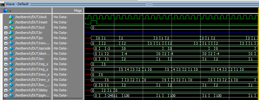
The design simulates correctly.
Verilog and simulation testbench
For the program:
5'h00: pgm = 16'b111_00010_001_00101 ; // set x 5 -- with delay 2
5'h01: pgm = 16'b101_00000_010_00_001 ; // mov x to y with no operation
5'h02: pgm = 16'b000_00000_100_00010 ; // jump Y-- to address 2
5'h03: pgm = 16'b000_00000_000_00001 ; // jump to address 1
The Y register should be repeatedly loaded with value 5, decremented, then reloaded. The simulation verifys this behavior.
The next step is to put it on the FPGA