"An audio spectrum analyzer that displays a real-time histogram-style visualization of the frequency spectrum of an audio input signal on a TV screen."
Our ECE 4760 final project was an audio spectrum analyzer that would display a histogram-style visualization of an audio signal. We were able to successfully display the frequency spectrum content of an audio signal in real-time using a black and white histogram visualization with bins arranged from left to right corresponding to low to high frequency ranges using a system based upon two Atmel Mega1284 microcontrollers.
The two microcontrollers handled separate tasks, with one performing the audio data acquisition and processing (hereafter referred to as the FFT MCU) and the other performing the visualization processing and video data transfer (hereafter referred to as the Video MCU). Users are able to select various display options using a set of push buttons including the overall frequency range displayed and the amplitude scale, among others.
Using a male-to-male 3.5mm audio cable, the user can connect any audio producing device such as a computer or MP3 player to the device’s 3.5mm audio jack and input an audio signal. Using a male-to-male RCA video cable, the user can connect any standard NTSC television supporting resolutions of at least 160x200 to the device’s RCA video jack and display the visualization on the TV.
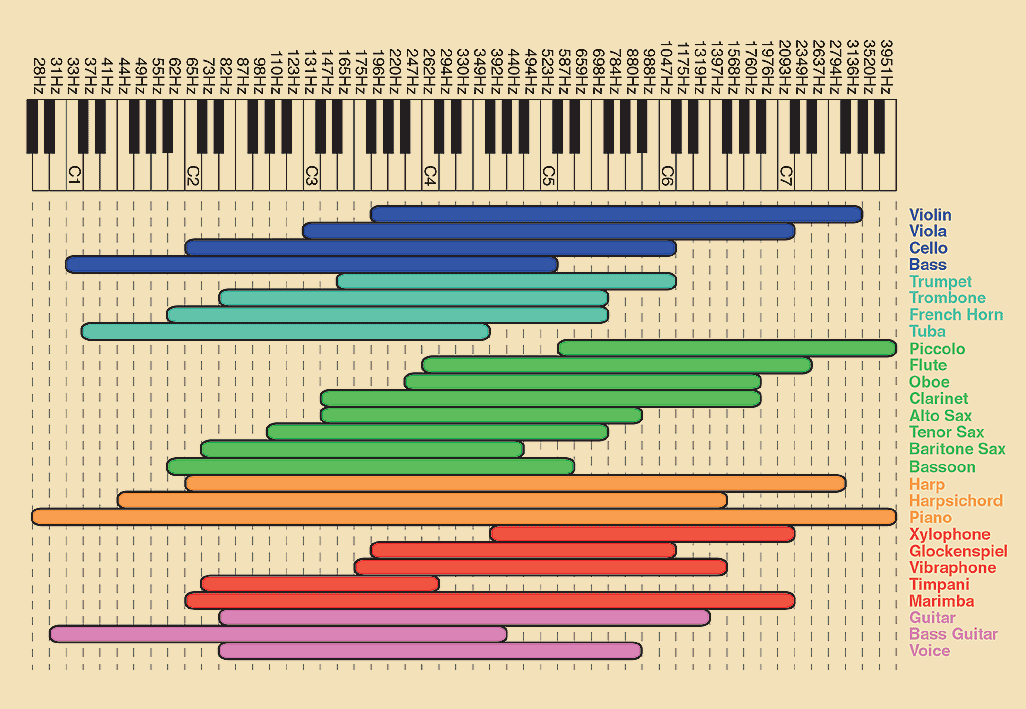
Our device is able to display frequencies in audio of up to 4 kHz, which covers the majority of the frequency range of typical music which is the intended input of our project, as shown in this diagram.
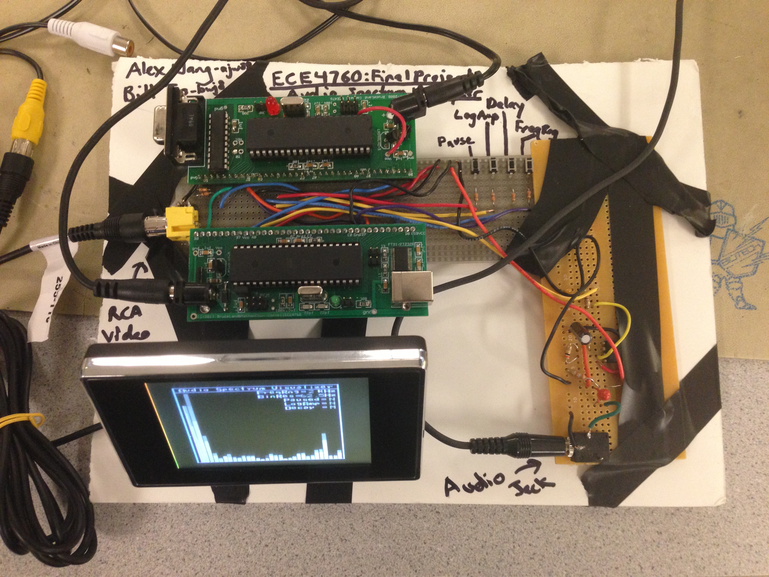
The final project.
High Level Design top
Rationale & Inspiration
Our project idea was inspired by popular toys such as the T-Qualizer, and built in music visualizers in many software audio players such as Windows Media Player. We wanted to create a similar hardware based equalizer that could be built cheaply and interface with standard audio inputs and video outputs. We originally wanted to take audio input with a microphone but realized that input directly from another device offers clearer signals. Being able to view a visualization of the frequency spectrum of audio is both interesting as a visual entertainment source to pair with music as well as a way to view the different frequency components assoicated with certain sounds or instruments. For example, one can see not only the main pitch of a note from an instrument such as a saxophone but also the various harmonics that determine the timbre of the instrument.
Overview
The data flow of our project runs rather linearly. First, the audio signal is inputted into the system through the audio jack. The signal is amplified and filtered and sent to the FFT MCU. This microcontroller will sample the audio signal at a constant rate and perform a Fast Fourier Transform (FFT) to convert the signal into frequency domain. This frequency domain data is transmitted to the Video MCU, which processes the data into a histogram visualization in real-time. Various user options can be changed via push buttons allow the user to modify the display as desired. Finally, the Video MCU transmits a composite video signal to the TV.
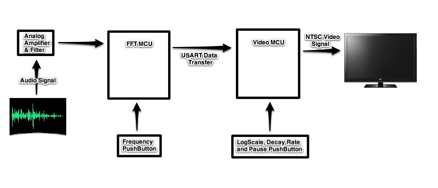
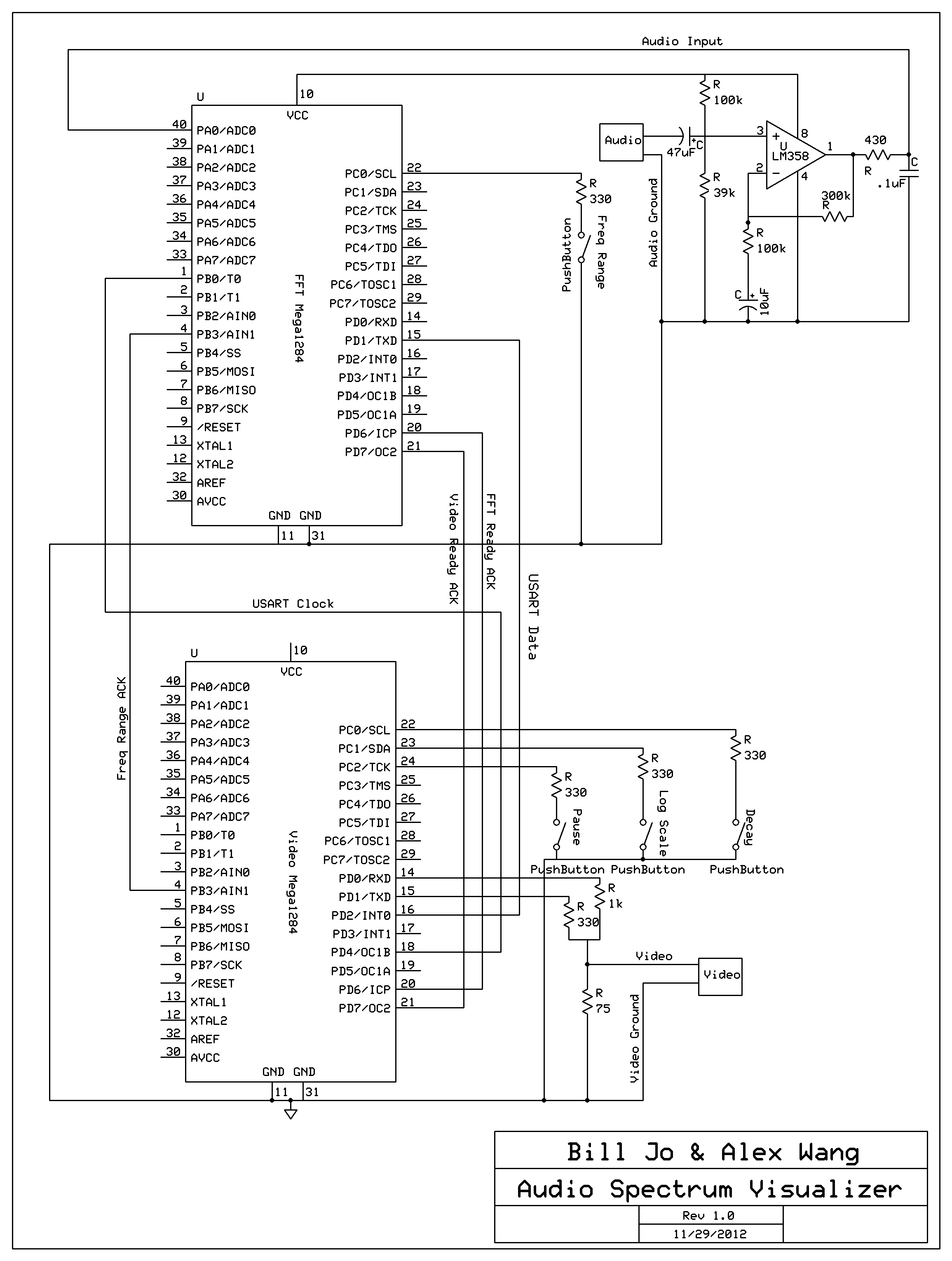
The block diagram for our project.
Hardware and Software Tradeoffs
The main hardware-software trade-off we faced was deciding whether to perform all of the computation on one MCU and complicating the software, or splitting the work between two MCUs and adding some more hardware complexity. Since the audio sampling needs to occur at precise intervals and the FFT must be done in an block type computation, its very difficult to balance that with the precise timing of the video display and the computation required to create the frame buffer while maintaining a fast, real-time process. We decided to split the two computations that required precise timing between two MCUs and delegate specific tasks to each MCU to handle by itself as detailed in the later software section. Splitting the work between the two MCUs required the extra hardware required to wire the two MCUs together as well as some extra software complexity to perform data transfer between the MCUs, but the added work is small compared to the complexities of trying to perform all of the software operations on one MCU.
Mathematical Background
In order to understand how the audio signal is sampled and processed into the frequency domain, one must understand several basic signal processing concepts.
First, we must understand how the sampling rate is determined. We used an ADC channel on the FFT MCU to sample the analog audio input into discrete digital values. According to the Nyquist Sampling Theorem, the sampling rate must be twice that of the highest frequency of the sampled signaled to prevent aliasing which will distort the signal. We decided on using 4 kHz as the maximum input frequency since this covers most of the frequency range in typical music without overwhelming the ADC. We set the ADC sampling rate to 8 kHz accordingly.
Second of all, we must understand how the audio signal is converted from its original time domain representation to a frequency domain representation. The Fourier transform is a mathematical algorithm that converts a time domain signal into its frequency representation. Various types of Fourier transforms are available depending on whether the input is discrete or continuous and whether the output is to be discrete or continuous. Since we are working with finite digital systems, we chose to use the Discrete Fourier Transform (DFT) which converts a discrete time audio signal of a finite number of points N into a discrete frequency signal of N points, referred to as frequency bins throughout this report because each point represents a “bin” or range of frequency content. With a purely real-valued signal such as our audio signal, the frequency representation of the signal is mirrored perfectly across the (N/2)th point in the DFT. The highest bin represents the frequencies up to the sampling frequency, and the lowest bin represents the frequencies just above 0. Each bin has the same frequency width, called the frequency resolution, which is the sampling frequency divided by the amount of bins N.
There are multiple algorithms that calculate the result of the DFT quicker than calculating the DFT directly using its defined equation (while maintaining the same exact result), called the Fast Fourier Transform or FFT. Many FFT algorithms exist, but the majority of them use recursive divide-and-conquer techniques that reduce the O(N2) computation time of the DFT O(Nlog2(N)). With large numbers of points N, this increase in speed is very significant in reducing computation time especially in software applications. Because of its recursive nature, it is usually necessary for N to be a power of 2. We use a fixed-point number based FFT algorithm adapted from Bruce Land in our software to convert our discrete digital audio signal into discrete frequency bins.
Standards
Several hardware and communication standards are used in our project. Regarding hardware standards, we used a standard 3.5mm phone connector jack socket to take in analog audio signals into our device. Our device is intended for a three-contact TRS (tip-ring-sleeve) type male connector to be connected to our female type jack. Although the three contacts allow for two channel stereo audio to be inputted, our device only uses one channel of the input and uses mono audio. We also used a standard RCA female video jack to output a composite analog video signal to a TV and is intended for a RCA male video plug to be connected to the jack. These two standard plugs are shown below.

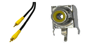
Left: 3.5mm plug and jack. Right: RCA composite video plug and jack.
Regarding communication standards, we used the NTSC analog television standard to output black and white video to our NTSC compatible television. NTSC (National Television System Committee) is the analog video standard used in most of North America. This standard defines the number of scan lines to be 525, two interlaced fields of 262.5 lines, and a scan line time of 63.55uS. The standards set by NTSC are closely considered in our project when creating the composite video signal to output to our TV.
While not technically a standard, we also used USART to serially transmit data between our two MCUs. The Atmel Mega1284 MCU has various frame formats that must be followed in both the transmit and receive MCUs including synchronous mode which we used. USART are often used with communication standards such as RS-232 but were not used in our project.
Hardware top
Introduction
The hardware portion of our project includes the two MCUs with USART connections, the hardware amplifier and filter circuit for the audio input, push buttons for user controlled input, and a DAC circuit for video output.
Audio Amplifier and Filter
First of all, we needed to calculate the input bias voltage offset for the analog audio signal to meet our requirements. There were two factors in this calculation: the range of the amplifier and the ADC reference voltage. The ADC reference voltage is the voltage corresponding to the maximum value of the ADC (255) and any voltages above this returned the maximum value. We knew that range for this amplifier was from 0-3.5V and ADC reference voltage had built in values of 1.1V, 2.56V, and 5V. We chose to use 2.56V because 5V gave us about half the resolution and values equating to voltages above 3.5V would never be used, and 1.1V would not utilize the majority of the range of the op-amp. Therefore, we decided to set the DC bias voltage to 1.28 to fully utilize the ADC range and to put the input signal within the op-amp range so that there are no negative voltages. To achieve this, we built a voltage divider using 100kΩ and 34kΩ resistors. Unfortunately, we were unable to find a 34kΩ resistor and opted to use a 39kΩ instead, raising our DC bias voltage to 1.4V.
We used the Texas Instruments LM358 op-amp as the main amplifier component. Using a non-inverting amplifier circuit, we set the gain of the amplifying circuit to 1+(300kΩ/100kΩ) = 4. Initially, when we were using the microphone as the input, we had the gain set around 10 to amplify the weaker audio signal when an external audio source was used (since the microphone needed its own voltage source to power itself, the microphone signal was much stronger than the external source’s signal). However, after we decided to exclusively use audio directly from an external audio source, we reduced this gain as these audio signals are larger and can be easily adjusted. We were frequently reaching the op-amp rail voltages with the gain around 10. We added an RC low-pass filter to remove frequencies above 4kHz to reduce aliasing. The RC time-constant corresponds to a cutoff frequency of about 3.7kHz, but it has a slow drop off and the RC filter transfer function doesn’t reach values below 0.5 until much higher cutoff frequencies, thus we wanted to set the cut-off slightly before our desired value of 4 kHz.
Below we see a video demonstration of how the analog audio signal looks after this stage on a oscilloscope.
Video demonstration of analog audio signal after amplification and filtering.
Push Buttons
Each push button had the same simple design. One end was connected to ground and the other to an input pin through a 330Ω resistor. The resistor was there to prevent any ports from being accidentally damaged from large current pulses. The MCU input had its pull-up resistor on, making the port (and button) active low.
Video Digital-to-Analog Converter
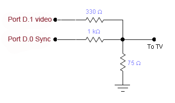
Video DAC circuit.
We used a simple DAC to combine the digital video data signal (Port D.1) and sync signal (Port D.0) to a composite analog video signal between capable of generating 3 levels: 0V sync, 0.3V black, and 1V white. This was achieved by the resistor network to the right.
The video output was connected to the inside axial pin of a standard female video RCA connector, and the outside ring of the RCA connector was grounded to the common ground of the entire device.
Data Transmission Connections
We used USART in synchronous mode to transmit data between the MCUs. This meant we needed a port dedicated to the clock and another port dedicated to data transfer from the FFT MCU to the Video MCU. There is no data transfer going in the other direction so a third channel was not implemented. Besides these channels, we also had 3 ports connected between the MCUs for communication of various flags and ready signals.
Color Generation
Color video generation circuit.
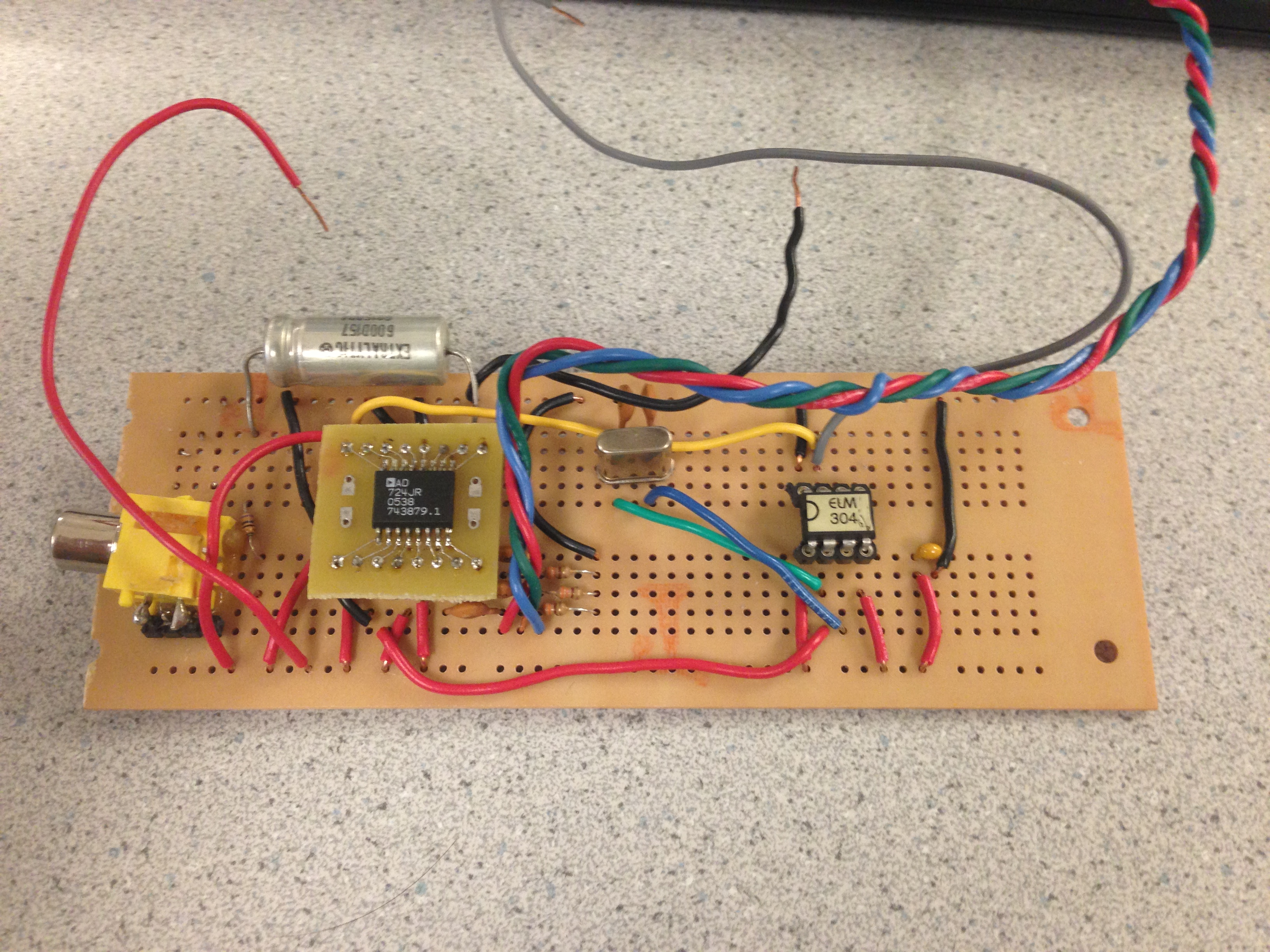
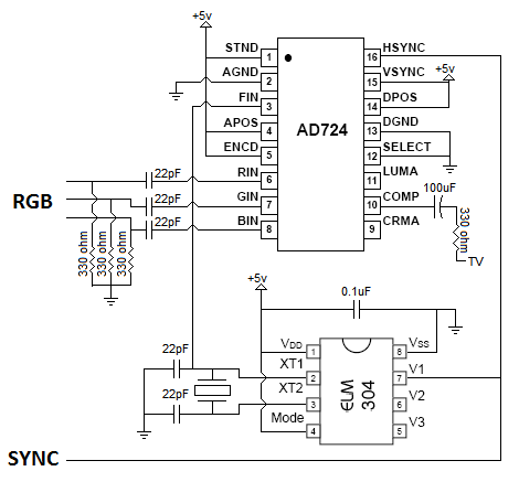
Initially, the goal was to make our project able to display color TV. The design was to use ELM304 for sync pulse generation, AD724 for converting RGB to composite NTSC signal, and the video MCU to output RGB values. The ELM304 sync output is wired to the HSync pin of the AD724 and 2 interrupt pins on the MCU. The MCU used these interrupt pins to figure out when to output RGB values depending on when the horizontal and vertical syncs happen. These RGB values are wired to the AD724 inputs and converted it into a composite signal which was wired to the TV. The circuitry featuring the ELM304 and AD724 and other components were created on a solder board but was never used due to difficulty in software (detailed in the software section). The schematic can be seen here.
Hardware Implementation
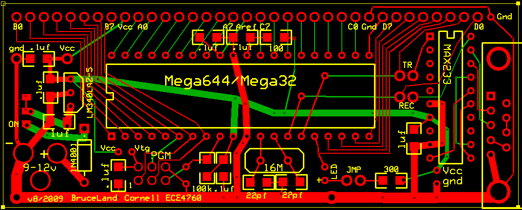
The Video MCU PC board was salvaged from lab scrap but required some fixes to make it work correctly. Specifically, a new voltage regulator had to be added to the board. The FFT MCU PC board was custom built from a PC board designed by Bruce Land and populated according to the specifications detailed on this page. Both were installed with the Atmel Mega1284 MCU. The final implementation used 2 solder boards. One board, the audio board, was used for the analog processing and included the amplifier, RC low-pass filter, and audio jack input. This board was powered by the FFT MCU. The second board, the main board, consisted of the two MCUs, 4 push buttons, video DAC circuit, and RCA video jack. The ground pins of the two MCUs were connected to each other as shared common ground, but the Vcc pins were kept separate as to avoid damaging the voltage regulators on the respective PC boards.
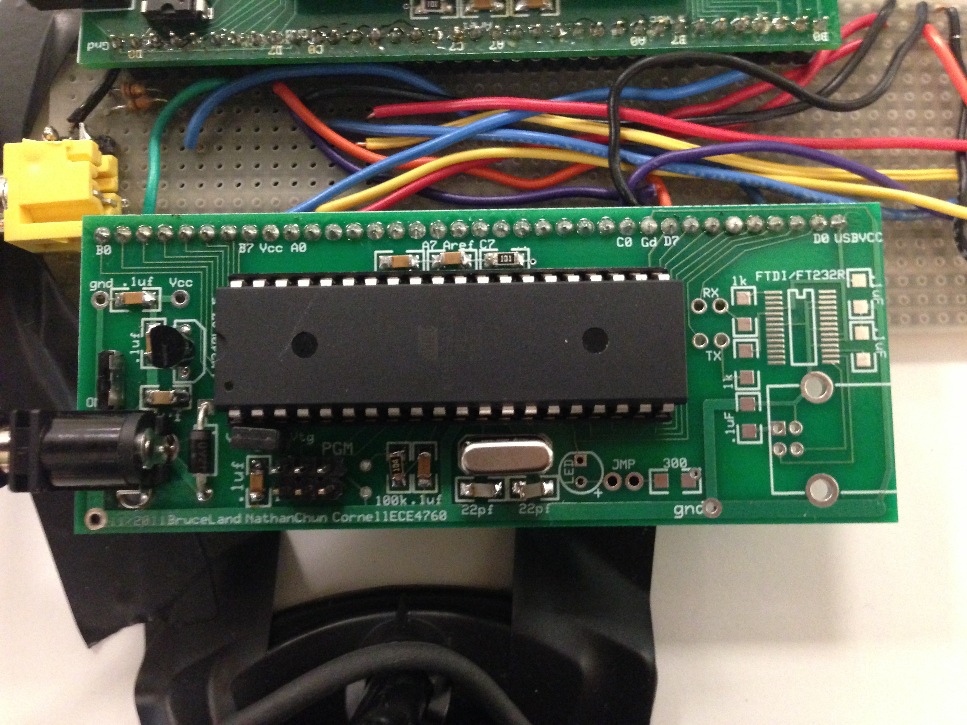
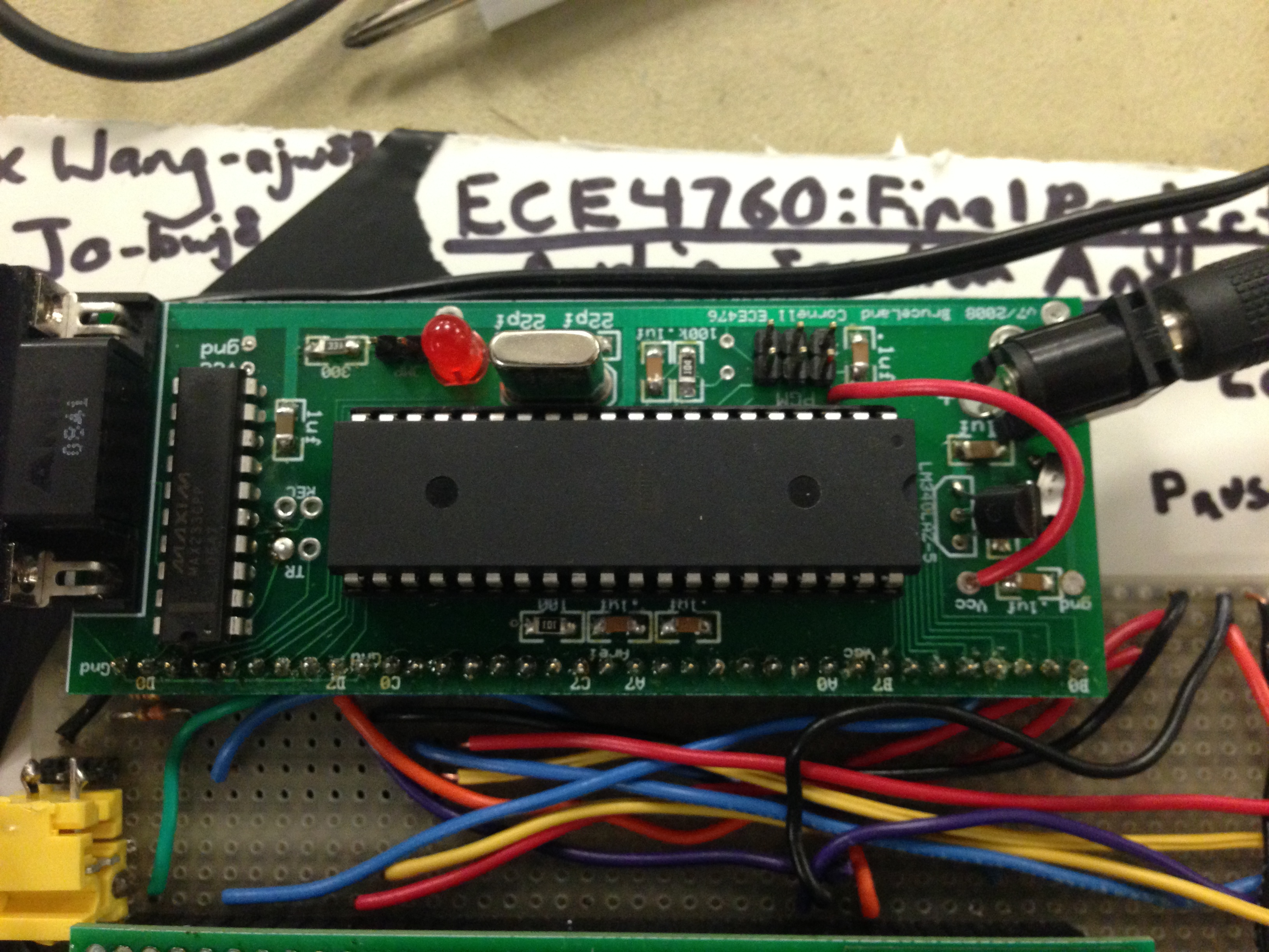
Left: FFT MCU PC Board. Right: Video MCU PC Board.
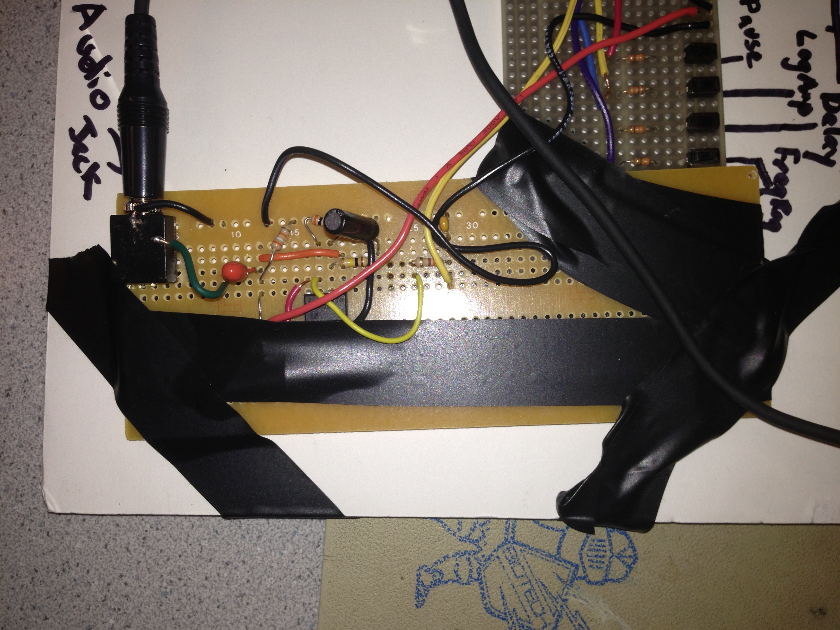

Left: Audio Board circuitry. Right: Main Board circuitry.
Software top
Overview
The software portion of our project was split in two between the code for the FFT MCU and the Video MCU. Both code segments were based off of the example code from ECE 4760 Lab 3 (FA12) as the oscilloscope required real-time operation that had periodic interrupt service routines (ISRs) that occurred extremely precisely at equal time intervals. The FFT MCU code performed ADC sampling of the audio signal, the FFT frequency conversion, USART transmission of the frequency data, and changing user options. The Video MCU was responsible for USART reception of frequency data, screen frame buffer preparation, video data transmission to the TV, and user option changes as well. Regarding our software setup, we used AVR Studio 4 version 4.15 with the WinAVR GCC Compiler version 20080610 to build and write our code, and to program our microcontroller. We also set our crystal frequency to 16 MHz and set option -Os to optimize for speed. To allow floating point operation, we included the libm.a library.
ADC Sampling of Audio Signal
The FFT MCU was responsible for sampling the modified audio signal from the audio analog circuit whose output was fed into the ADC port A.0. In order to get accurate results, we must make sure to sample the ADC port at precisely spaced intervals. Since the ADC is running at 125kHz and it takes 13 ADC cycles to produce a new 8-bit ADC value (ranging from 0-255), or about 104us. The ADC was set to execute at 125 kHz to allow 8 bits of precision in the ADC resulting value (according to the Atmel Mega1284 specifications), which we deemed sufficient for our purposes. Our ADC was set to “left adjust result”, so all 8 bits of the ADC result were stored in the ADCH register. At a sample rate of 8kHz, an ADC value will be requested every 125uS, which means there should be sufficient time for a new ADC value to be ready each time it is requested. The sample rate was set to be cycle accurate at 8 kHz by setting the 16 MHz Timer 1 counter to interrupt at 2000 cycles (16000000/8000=2000), and having the MCU interrupt to sleep at 1975 cycles (slightly before the main interrupt) to ensure that no other processes would be interfering with the precise execution of the Timer 1 ISR where the ADC is sampled. The ADC voltage reference was set to 2.56V to allow a good signal range as the input signal was DC biased at 1.4V. To remove the DC offset, we subtracted the results of the ADC by 140 (which corresponds to about 1.4V). The final range of signed ADC values are -140 to 115, which does not deviate too far from the ideal range of -127 to 128 which would have been chosen had our analog DC offset been exactly 1.28 as we desired. This non-ideality does not have too much significance since the majority of the time, our input signal does not reach these extreme end values. However, when sufficiently large signals are introduced, its noticeable that the negative signals are slightly larger than the positive since they are clipped at -140 and 115 accordingly.
FFT Conversion of Audio Signal to Frequency Bins
The ADC values were stored in a buffer of length 128 as our fixed-point FFT code is maximized at a 128-point operation since the program would crash due to memory overflow for any larger FFT. We wanted to have the largest amount of points possible as this would result in more frequency bins and a more accurate frequency representation of the audio signal (and as we see in our results, still allows real-time calculations). This value of 128 is parameterized as N_WAVE in the code. We utilized unmodified code written by Bruce Land (who in turn had modified the code from the work of Tom Roberts and Malcolm Slaney) that performed an in-place FFT with fixed-point number arrays. The code, which was a subroutine called FFTfix, took two arrays of length 128, the real and imaginary components, and the base 2 logarithm of 128 for the number of FFT recursions/iterations to complete. This code would perform a forward transform from the time domain to the frequency domain of the input real and imaginary arrays (which represent the two components of a complex input array), and return the result in place in the same arrays that were inputted. The numbers used would be fixed-point 16-bit numbers (stored in an int variable type), where the high order 8-bits represent the integer digits and the low order 8-bits represent the decimal digits. The code required a table of length 128 of one cycle of a sine wave to be executed in order to run the FFT and was initialized in our main method. Since our input array is purely real, I also initialized a 128 length zero vector to represent the imaginary component of our input. The borrowed code from Bruce Land also included several fixed-point number operation macros that perform multiplication and convert various data types to fixed-point format.
Our main method of our program continuously waited until the ADC buffer was filled to 128 samples, and then it immediately started the FFT operation. First, the imaginary buffers from the previous FFT operation were zeroed out, and the ADC buffer was copied into an array representing the real input (for data integrity concerns since the FFT operates in place). We decided to window the real array with a trapezoidal mask with side-slopes of 32 points as we wanted to remove any sharp cutoffs at the end of the ADC buffer which introduce high-frequency content. We do this because ideally we want our ADC input to be infinite and continuous but our Fourier transform must be finite in implementation, and having cut-offs at the edge values of our input signal can potentially be seen as a sharp discontinuity by the FFT, so we want to smooth out this sharpness by decreasing the amplitude of the edges gradually (which won’t affect the frequency content of the signal).
We first copy the ADC values into the bottom 8-bits of the 16-bit fixed-point number that represents the real portion of the FFT input. This was then shifted left by 4 to increase the values of the FFT output. Therefore, the ADC values were copies into bits 5-12 of the 16-bit number. Since all of our ADC values are purely integers and the fixed-point FFT does not know whether our input is decimal valued or not, it does not really matter where our number sits bitwise in the 16-bit fixed-point number as the end result will be read as an integer and not a fixed-point number. This real input array and a zero-ed out imaginary input array were the inputs into FFT.
We wish to only use the magnitude information of the frequency content of our signal, thus we take the magnitude of our frequency content by taking the sum of the squares of both the real and imaginary frequency outputs. Technically to take the actual magnitude, we should take the square root of the sum of squares, but since this is just a scaling factor and the frequency content was too low in magnitude anyways, we just left it as the sum of squares.
We discovered in our first implementation of the FFT code many of our operations were being done with integer operations and not fixed-point operations, thus our frequency magnitude data was incorrect and caused our output to look “noisy”. After switching to the fixed point operations by using the provided fixed-point macros, our output was much cleaner and representative of the actual frequency content of our audio signal. We tested this by hardcoding a sinewave signal with known frequency and viewing the frequency output to see if there was only one non-zero frequency bin.
Since the frequency content is mirrored across the middle of the output in a FFT when the input is purely real, only the first 64 points of the 128 point output were relevant and stored. These 64 points represented frequency bins with frequency resolution of 62.5 Hz as our maximum frequency resolved is 4 kHz (4kHz/64=62.5Hz). We wished to only transmit and display 32 frequency bins, so depending on the frequency range the user wished to display we either paired and combined adjacent bins to form 32 bins of 125 Hz resolution (0-4 kHz range), or we only transmitted the first 32 bins (0-2kHz range). To simplify the USART transmission to the Video MCU, we stored only the bottom 8-bits of the resulting magnitude (into a length 32 8-bit array) since our USART transmission used 8-bit character size.
Once this frequency magnitude content array was prepared, we were ready to transmit the data to the Video MCU, which will be detailed in a later section below. Before we fully implemented the data transfer and Video MCU code, we first tested the output of our FFT by simply outputting the 32 bin values as a text string using UART (UART code provided by the ECE 4760 course, as seen in Lab 1 of FA12) through the USB port on our PCB to our PC using a serial connection at 9600 baud and viewed the output using PuTTY. This text based output allowed us to verify the FFT MCU code in isolation before the rest of our code was fully implemented. After data transmission, we set the ADC index back to 0 so that the program could start to sample ADC values again into the ADC buffer, overwriting the old buffer’s values.
User Option Changes
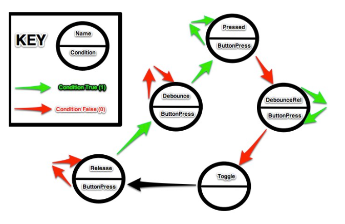
Button Press FSM Diagram.
The FFT MCU has one button (frequency range) and the Video MCU has three buttons (pause, amplitude scale, and decay speed). Theses push buttons are connected to Port C of both FFT and Video MCU. For the pins of Port C connected to push buttons, they were set to input and their pull-up resistor were enabled, making the pins active low. The values of the pins were polled in every iteration of the main loop, which ran often enough to ensure fast and valid button presses. After polling Port C, it stores the value of the pins and updates the button press FSMs. Each push button has its own FSM, and the states of all of the FSMs are nearly identical, differing only in the user option they change. The button press FSM has 5 states, which are detailed in the diagram below (shown to the right). The FSM starts in the Release state, and if the port connected to the button is read to be active, the FSM moves to the Debounce state. In the Debounce state, we see if that port is still active, and if so we move to the Pressed state (if not, we move back to the Release state). In the Pressed state, we check if the port is still active, and spin in this state until it is released, in which we move to the DebounceRel state. In the DebounceRel state, we check if the port is still active and if not, we move to the Toggle state (and if so, back to the Pressed state). In the Toggle state, we toggle the value of the corresponding user option flag, as well as the value of the label to print on the screen. For the decay speed option, instead of toggling the speed, it cycles between slow, medium, and fast decay speeds. Frequency range option was treated slightly differently since it affect both MCUs and not just the FFT MCU. When a valid press is registered, the Video MCU let the FFT MCU know of this button press by toggling the value of its Port B.3, connected to Port B.3 on the FFT MCU. This allows both MCUs to “be on the same page” so the frequency data transmitted can be treated correctly. The FSM then immediately returns to the Release state.
USART Data Transmission and Reception
We opted to use USART in Synchronous mode to transfer the frequency magnitude bin data from the FFT MCU to the Video MCU in our project. USART is a simple serial communication protocol that utilizes at minimum one transmission wire to send data from one MCU to the other. We decided to use synchronous mode for our transmission as we wanted a separate transmission clock line to maintain proper timing synchronization in both transmission and reception in both MCUs without the extra timing overhead required by asynchronous transmission to maintain the same timing. Each MCU has two USART channels, each with a transmit and receive port as well as a clock port if synchronous mode is enabled, thus USART is a three-wire protocol. We used USART channel 0 to transmit from the FFT MCU and USART channel 1 to receive on the Video MCU (USART0 was used for video display). The USART was set to transmit with 8-bit character sizes, which takes a byte and transmit 8 bits serially. The USART frame in synchronous mode initially has the transmission line set to high when idle, and transmits a start bit by setting the line low for one cycle. It then transmits the 8 bits in 8 cycles, and completes the character transmission with a stop bit by setting the line high again. It can then immediately start another frame by going through the same process, or it can keep the line idle. USART offers different frame formats including different character sizes, parity bits, and multiple stop bits, but we opted to use a 10-bit frame for simplicity and speed of transmission with 1 start bit, 8 character bits, and 1 stop bit.
We had various difficulties in implementing the software portion of our data transmission, first of all in choosing the transmission protocol to use. We had initially tried USART in SPI mode, but we realized that only Master mode was available in our MCUs, and we wished for the Video MCU to operate in Slave mode as it was dependent always on whether the FFT MCU was ready to transfer. We decided on the previously mentioned protocol and frame format because it offered the simplest transmission method with the lowest overhead.
Second of all, we had to synchronize when the data was actually transmitted because the two MCUs were not always ready to transmit/receive when the other MCU was ready, and USART allows the MCU to transmit without the other MCU being ready. The FFT MCU was only ready to transmit when a full frequency data buffer was completed (ADC sampling and FFT data prepared), and the Video MCU could only receive data when it was not transmitting data itself to the TV screen (during the “blank” lines of the TV as detailed in the Video Display section) in order to preserve the real-time TV signal. Thus, we needed to have external “ready” lines between the two MCUs to tell the other MCU when it was ready to transmit/receive. Port D.6 on both Video and FFT MCU is the Tx ready line. Port D.7 on both Video and FFT MCU is the Rx ready line. When the FFT MCU finishes preparing the frequency data, it sets Port D.6 to high and waits for Port D.7 from the other MCU to be set high. The Video MCU will check once it reaches a blank line whether Port D.6 was set high and whether its frequency bin buffer is full. If both conditions are true, it sets Port D.7 to high. At this point, the FFT MCU will proceed to blast a 4 byte packet to the Video MCU by loading the UDR0 data transmit buffer. The Video MCU will receive a byte as soon as it set Rx ready by reading the UDR1 data receive buffer (and storing the byte in its own frequency bin buffer). Once that first byte is received, it sets Rx not ready to ensure Video MCU does not send the next 4 bytes. It will continue to receive the 3 other bytes that the FFT MCU sent, and then it will proceed to the next video line. We send the data in 4 byte packets because each video line only has 63.625us to complete all of its operations, and we do not want any data loss at all due to lack of operation time because it will put the two MCUs out of sync (and both the sync and data loss are irrecoverable in our transmission format). On the next available blank video line, the same pattern happens again and 4 more bytes are transmitted until all 32 bytes of the frequency data buffer are transmitted. Once it finishes the last byte transmission on FFT MCU side, it sets Tx not ready by setting Port D.7 to low.
Our USART data transmission was set to operate at 2 Mbps, as the USART timing guidelines requires the transmission rate to be less than 4MHz (the system clock frequency 16 MHz divided by 4). We initially tried the transmission rate to be at 4 Mbps, but that caused intermittent artifacts to be transmitted, so we lowered the rate to the next highest available rate which was 2 Mbps. We wanted to maximize the transmission rate in order to prevent the transmission of 4 bytes from taking more than 63.625us (which should ideally take only 16us, but leaving a good time margin ensures data transfer integrity).
Video Display - Screen Buffer Preparation
The Video MCU was responsible for displaying the frequency bin data received from the FFT MCU as a histogram style visualization in real time. To start off, we first initialize the display by printing all static elements of the display to the screen which includes the borders of the screen, the title bar and message, and the user option value labels. These static elements are created with a video display API borrowed from the example code in Lab 3 of ECE 4760 FA12. This API includes subroutines such as video_pt which draws a pixel at a certain location, video_line which draws a line between two chosen locations, and video_puts which writes a text string at a certain location using an included preset array of different characters and symbols. We store this initial screen into a buffer called “erasescreen” that we use to erase the screen at the start of a new frame. Clearing the screen with the static messages included reduces flicker on the static elements that will always be printed on the screen and saves computation time. When a full 32 byte frequency bin buffer has been received (and if the device is not set to paused), the program will start to load the new screen frame buffer to be transmitted to the TV by first clearing the screen. It will then iterate through each of the 32 bins (except the first bin, since we don’t want to display the bar corresponding to mostly DC content and low frequency non-audible sound), and display a vertical bar at position of that frequency bin whose height corresponds to the value in the bin. Low to high frequencies were displayed from left to right. We display the 4 pixel wide vertical bars by drawing 4 adjacent vertical lines using a subroutine called video_vert_line that we adapted off the borrowed video API’s subroutines video_pt and video_line. We decided to create our own subroutine because using video_line to draw only vertical lines was computationally expensive and slows our frame rate significantly since video_line provides capabilities of drawing lines at angles. Our code simply writes white pixels from the bottom of the screen to the requested height using a simple loop and is very computationally efficient. Between each bar we leave a 1 pixel gap to differentiate between the bars, thus we need 154 pixels horizontally of our 160 pixel wide screen to display all 31 frequency bins.
To calculate the height of our bars, we had to account for the height of our screen (200 pixels) because the vertical positions are inverted with higher physical positions corresponding to lower y position values. Thus any height we wanted to display was subtracted from 199 to create the y position (199 instead of 200 because we can’t display in the lowest pixel since our border is there).
We wanted to allow the user to display the frequency bin magnitudes on both a linear and logarithmic amplitude scale depending on the value of the user option selected. For the linear scale, we simply just displayed the received value from the FFT MCU. For the logarithmic scale, since logarithms are slow to compute and we know our values range only from 0 to 255, we precomputed all 256 of the logarithm values in an array initialized at the beginning of our program and simply used the received values to index into this array to get the logarithmic value to display. The logarithm table is created using the natural log function on all values from 0 to 255. This led to a logarithmic scaling of the magnitudes which puts more weight on the lower amplitude values and less weight on the higher amplitude values. However, the overall magnitude of all of the values are much lower, so we scaled the values up by multiplying by 45 so that the highest value in the array corresponds to the greatest height in the screen, and then subtracted by 30 so that the lowest value corresponds to the lowest height in the screen. This type of display matches human hearing, which is logarithmic.
We also implemented a software RC decay for our display to make it easier to follow the different bar animations and isolate certain frequencies by “slowing” down the quickly changing display. When a new frame is loaded and a new value for a bar is ready to be displayed, we first check if the new value is greater or smaller than the previous value. If it is greater than the previous value, we simply display that value. If it is smaller however, we display the last value of the bar subtracted by a user selected fraction of that value. This creates an RC decay for the bars in that if the bar value drops from a high value to a low value, it will do so gradually over several frames instead of immediately in the next frame. Bars will stay on the screen long enough for the user to view and isolate certain frequencies. We implemented an user option to vary the speed at which the decay occurs.
After preparing the screen frame buffer as mentioned, we reset the index of the frequency bin buffer so that a new buffer can be received from the FFT MCU. In addition to the frequency bin bars, the value of the user options were also dynamically updated each screen frame buffer. Using the video_puts function from the video API, we displayed the text string matching the current value of each of the user options available. This was updated at the end of each screen frame buffer update with the values set in the button press FSMs.
Video Display - Data Transmission to the TV
As the screen buffer is being prepared, we are simultaneously blasting data to be written to the screen at a constant precise rate defined by our version of the NTSC TV standard. We based our code largely off of the ISR from Lab 3 (ECE 4760 FA12), where we transmitted data to the TV screen in a nearly identical manner. We used a method similar to the NTSC standard except with no interlacing and use only 262 lines. The video signal consists of a sync signal and a video data signal which are combined using a DAC (detailed in the hardware section) and outputted to the TV unit. Each line consisted of a horizontal sync pulse (4.7uS), a black non-visible region hidden by the TV called the back porch (5.9uS), a visible region (51.5uS), and finally a black non-visible region called the front porch (1.525uS), for a total of 63.625uS. These steps are repeated for each of first 247 lines. At line 248, it begins the vertical sync to initiate the next frame to return to the top left corner of the screen. From lines 250 to 262, the signal returns to regular sync but there is no data written. After line 262, the program cycles back to line 1 and this frame is completed.
To ensure precise NTSC video timing, we initiated Timer 1 ISR to interrupt precisely every 63.625uS or every 1018 cycles, (63.625uS*16MHz=1018 cycles). As was done to maintain precise ADC sampling in the FFT MCU, we used a second ISR that interrupts slightly before the main ISR (at 999 cycles) to put the MCU to sleep so that the main ISR will always execute without interruption. In the ISR, we first setup the sync signals (by writing the appropriate bit to Port D.0, the sync signal) and back porch as described in the previous paragraph. We then decide whether to display video data or not in the visible region. We decided to use a screen resolution of 160(H)x200(V) in our project, so only 200 of the 262 lines actually had data displayed in the visible region, which are lines 30-229 in our code. In lines 30-229, we have precisely 51.5uS to send 20 bytes of data (160 pixels) to the TV screen. We decided to use USART in SPI Mode (MSPIM) to blast video data continuously at 4MHz to the TV screen through Port D.1. At a 4 MHz transmission rate, each byte of data transferred takes exactly 2uS to be transmitted to the TV screen, so we need exactly 40uS to transmit this data without any delay between any of the bytes so that the image does not tear or artifact. We blast the data to the screen by simply writing 20 bytes from the screen buffer (that correspond to the data in a single line) one by one to the 8-bit UDR0 USART transmission register.
In the other 62 “blank” lines where we do not display anything in the visible region, we decided to use this time to receive data from the FFT MCU as detailed in the USART section.
We had originally wanted to implement color video in our TV unit, and we had fully created the hardware portion as detailed in the hardware section to generate the relevant signals for color video generation. However, the code from previous ECE 4760 projects that we wanted to base our code off of was written for the CodeVision C compiler. We deemed it too time consuming to translate the lengthy code to work for the GCC compiler that the rest of our code uses, and we found color video generation to add little value to the overall final product of our project. Thus we decided not to implement color video generation in our project, and we kept our video generation in simple black and white.
Results top
Overview
Overall our project performed very well for a wide range of music, and it was very obvious that the project was working when we saw the bars move along with the pitches in the music and have amplitudes corresponding to the volume of the music. The user options chosen by the user could be selected to optimize the visualization to match the speed and volume of the music. Below we see three video demonstrations of our project visualizing songs from different genres, speeds, and volumes.
Slow music: Blue Danube Waltz by Johann Strauss II.
Medium music: Shadow Days by John Mayer.
Fast music: Scary Monsters and Nice Sprites by Skrillex.
Real-Time Operation
The real-time portion of our project was achieved so that a new sound sample would appear on the screen without any noticeable delay so that what is being visualized on the screen matches the audio being played at the same time. The worst case latency of a obtaining the frequency data for a frame is about 51.2 ms, much faster than the average human reaction time (215 ms). Latency for our system is the sum of the amount of time to do the 128 ADC samples at 8 kHz (16ms), time to compute the 128 point FFT (5.8ms), the data transfer time (62 lines *63.625us/line = 3.94ms), twice the video display time (2 * 200 lines * 63.625 us/line = 25.45ms). I doubled the video display time because the data transfer must wait for the video MCU to finish displaying the current frame. After data transfer occurs, it takes another frame time to transmit the frame to the screen. Thus, the throughput of the frequency data is at worst about 19 Hz since as soon as the data transfer finishes, the ADC starts to sample again. This means that the time to convert the frequency buffer into the screen frame buffer is not included since the ADC does not wait for the new frame to be converted before it starts to sample again.
Video Output
The refresh rate of our video output was variable depending on the process power consumption of the user options chosen. When the screen refreshes very quickly, the screen appear flickery or lighter towards the right of the screen but this is not due to any error in the code, but rather due to the way our screen is written from left to right. There are no random shifts, artifacts, or other glitches in the TV screen, verifying that our video signal timing met NTSC requirements. A small concern was the status of the user options printed in the top right of the screen sometimes flicker because the screen erases them shortly after the strings were written so they appear to flicker or not stay on the screen very long. We could have avoided this flicker by making the user option values update only when they were changed and kept them static otherwise, but this would require the labels to be printed in a static region of the screen where bars could not be displayed. After considering the trade offs, we decided that it was not worth it to scale all of the bars down and waste screen space in order to make the user option labels slightly more appealing.
FFT Accuracy
The accuracy of our FFT was tested by inputting sine waves of pure frequencies. A single frequency signal tended to display as a single large bar with two smaller bars on each side. Ideally, we expect the result to display only a single large bar, but our audio signal processing computes with some error involved. These errors are introduced from our fixed-point calculations, the finite nature of our signal, and the discrete nature of our signal. The fixed-point calculations may have introduced error in that decimal point accuracy may be lost since only 4-bits are available to store decimal values. The finite nature of our time signal may have caused truncated cycles of the sine-wave at the edges of the 128 point signal where the sine wave did not complete a full cycle and was truncated, leading the FFT to calculate other frequencies. Finally, the discrete nature of the ADC sampling may lead to errors in calculating the frequency of what was once a continuous analog signal of a pure frequency, and may lead to other frequency components being present.
Despite the small error in our FFT accuracy, the bars are always centered and greatest in magnitude at the frequency location we expect when we play pure frequency sine waves. When we do a frequency sweep from 0 to 4 kHz, we see a bar sliding horizontally right across the screen as expected. This is shown in the video below.
Video demonstration of frequency sweep from 0 to 4 kHz of a pure sine wave inputted to our device.
Safety
There were no major safety concerns in this project as we did not use any mechanical parts, high voltages, or wireless transmission in our device. The only output of our project is through the TV screen, which has a safe refresh rate below 30 Hz and whose brightness levels can be adjusted to a safe level.
Interference
As all of our communication and circuitry in our project was through wired means, we do not foresee any major interference with any other devices.
Usability
There are not many major usability concerns as the user interface is minimal. The only user interface is through the 4 push buttons that toggle the different display options. The display options are shown in the top right corner of the screen with their value updated in real time as they are changed. The 4 push buttons are arranged physically on the board in the same order as the labels are displayed on the screen. The labels are slightly abbreviated to fit in the screen, but their meaning should be somewhat self-explanatory to most users. A table to explain the labels is shown below.
| Label | Meaning | Value |
|---|---|---|
| FreqRng | Overall Frequency Range | “2kHz”: 0 to 2kHz range, “4kHz”: 0 to 4kHz range |
| BinRes | Bin Frequency Resolution | “62.5Hz”: 62.5 Hz resolution, “125Hz”: 125 Hz resolution |
| Paused | Pause/Play | “N”: Play, “Y”: Paused |
| LogAmp | Linear or Logarithmic Amplitude Scale | “N”: Linear Scale, “Y”: Log Scale |
| Decay | Bar Decay Speed | “S”: Slow, ”M”: Medium, ”F”: Fast |
Conclusions top
Summary
The final results of our project were extremely satisfying as we were able to meet the majority of our expectations set in the project proposal. We were able to implement a fully functional audio spectrum analyzer that ran in real time and accurately displayed the frequency content with a histogram visualization of the input audio. We also were able to keep the material costs down and make it user friendly, as detailed in the parts list in the appendix. By using standard 3.5mm audio jacks and RCA composite video jack, any user with a music producing device, standard auxiliary audio and video cords, and NTSC-compatible TV could use our product. The added user options through the push button interface also added to the quality of the visualization as well as introduced the ability to personalize the display. This project not only allows the users to view their favorite music in a fun and interactive fashion, but it also offers information about their music otherwise unaccessible.
Future Improvements
Future improvements that we considered implementing in our design but could not due to time-constraint include color video output, the ability to select certain user-defined frequency ranges and bin resolution, different visualization types, and volume control.
The color video output could have been implemented in software as mentioned before if we had the time to translate the CodeVision code from previous student projects into GCC compiler compatible code. The color video could have enhanced the visualization by using certain color levels to indicate certain amplitude levels, and a color gradient could be implemented vertically across the bars. Since we had already created a working hardware circuit to implement color video, this definitely could have been implemented with another one or two weeks time.
We also considered introducing the ability for the user to focus on certain user-defined frequency ranges with user-selectable bin resolution so that certain frequency ranges of interest could be analyzed with greater precision. This would have required multiple hardware filters as well as being able to dynamically change the sampling rate to match the desired range and resolution.
We considered adding different visualization styles other than the histogram style. With more time, we could have implemented various other types of visualizations inspired by those already created in software visualizers such as Windows Media Player.
Finally, we considered implementing a volume control on our device. Sometimes the input signal from the external audio source was too low or high in amplitude and the bars on our visualization would be too low or high. We could tune the gain on the amplifier by replacing the one of the resistors in the amplifier circuit with a potentiometer and allow the user to modify the gain of the signal until fit. Currently, the volume has to be modified on the external source.
Conforming with Standards
The only standard relevant to our project was the NTSC analog television standard. We conformed to the standard by using fields of 262 scan lines. We decided to not interlace our fields, and used frames of only 262 scan lines instead of the 525 scan lines as recommended by the standard. We did this by skipping every other 262 line field, and only displayed a frame on 262 of the 525 interlaced lines. By not interlacing and skipping every other field, we simply had a slower field rate of 30 Hz instead of the 60 Hz suggested by the standard, but our frame rate was still 30 Hz. Each one of our scan lines displayed in 63.55uS, and was formatted to the timing specifications detailed by the standard (sync, back porch, visible region, front porch). The analog composite video signal was created using a DAC with the appropriate voltage levels for the sync, black, and white levels.
Intellectual Property
There are several intellectual property considerations regarding our project. First of all, the code to calculate the FFT was adopted from code provided by Bruce Land. This code was originally authored by Tom Roberts and improved by Malcolm Slaney from whom Bruce Land received the rights to use and modify for the example code that we adopted. The video portion of our software was based on example code written in part by Shane Pryor, David Perez de la Cruz, Ed Lau, and Morgan D. Jones, all of which was modified and adapted for the Mega1284 by Bruce Land. This same section also contained portions of our own code from Lab 3 in ECE 4760 Fall 2012. Some sections of this website and report are also adapted from our own write up for Lab 3 of the same course. The color circuit, which we never used, was based on final project designs by Matthew Pokrzywa, James Du, and Alan Martin Levy. All diagrams used are our own work or from the course website. All videos used in this website are our own work as well, and the audio snippets playing in the videos are property of their respective artists and are used solely for demonstration purposes and not personal gain. The template from this website is adapted from the website for the “Pace Clock” final project of Paul Swirhun and Shao-Yu Liang, who in turn adapted their website from a Cornell University provided template. All of the borrowed intellectual property is referenced in the Appendix, and borrowed due to the fact that it was provided by the course content or instructor.
Ethical Considerations
During the course of working on this final project in ECE 4760, we made sure to follow the IEEE Code of Ethics with strict accordance. We ensured that both ours and other’s safety were never compromised while working on the project. Furthermore, there are no safety issues involved with the use of our project by any users, including unskilled users. We began the task only after we were sure of a good and attainable design that was reviewed not only but us but also by the instructor and teaching assistants. This is to ensure we were competent in engineering the project we were about the undertake. We accepted but also seeked constructive criticism from our peers and superiors to make our project better in any and all ways. We treated all of our peers with respect and did not say or publish anything offensive while in lab. We were respectful to others wishes and used headphones for music when possible. We did not use anyone’s work without asking. We cited all contributions made to the project including any of our own previous work. Lastly, we accept any and all responsibilities in all issues related the project we created and believe that this report represents an honest description of the results of our project.
Legal Considerations
There are no major legal considerations to be concerned as we did not infringe upon any intellectual property and our project does not pose any known danger to any people or property. We use standard 9-12V AC adapters to power our design, all of which should conform to legal standards.
Appendices top
A. Source Code
B. Schematics
Below are the schematics for our project and the PCB layout for the Video MCU board (the layout for the FFT MCU board is slightly different, but unfortunately unavailable). The schematic was created using ExpressPCB, and the layout file can be downloaded here.
Final Schematics Diagram
PCB Layout for Video MCU Board
C. Parts List and Costs
The total budgeted cost for our project is $36.65. All of the parts from our project were obtained from the lab, whether from lab stock or salvaged from previous projects or scrap piles. Rented refers to a part used from the lab to be returned after the conclusion of the project. Lab Stock refers to parts used from lab inventory for permanent use. Salvaged refers to free parts that were taken from scrap piles and/or previous projects. No parts were bought from vendors.
| Part | Cost/Item | Method Obtained | Quantity | Total Cost |
| Atmel Mega1284 Microcontroller | $5 | S | 1 | $10 |
| LCD TV | $5 | R | 1 | $5 |
| SIP/Header Pin | $0.05 | S | 1 | $8.15 |
| DIP socket | $0.50 | S | 2 | $0.50 |
| Custom PC Board | $4 | S+F | 1 | $4 |
| 6 inch Solder Board | $2.50 | S | 5 | $5 |
| RCA Video Jack | $1 | S | 1 | $1 |
| RCA Video Male-to-Male Cord | $1 | R | 4 | $1 |
| 3.5mm Audio Jack | Free | S | 2 | $0 |
| 3.5mm Male-to-Male Audio Cord | $1 | R | 147 | $1 |
| 3.5mm Audio Splitter (Male to 2x Female) | $1 | R | 10 | $1 |
| Push Button Switch | Free | S | 1 | $0 |
| Texas Instruments LM358 Op-Amp | Free | S | 1 | $0 |
| Resistors & Capacitors & Wire | Free | S | 5 | $0 |
| Key for “Method Obtained” | --- | --- | ||
| R=Rented, S=Lab Stock, F=salvaged/free | TOTAL | $36.65 |
D. Division of Labor
| Bill Jo | Both | Alexander Wang |
|---|---|---|
| Video Generation Code | Design Research | Audio Sampling and FFT Data Processing Code |
| Audio Solder Board | HW & SW Debugging | USART Data Transmission Code |
| Hardware Schematics | Website Content | Main Solder Board |
| Color Generation Solder Board | Website Formatting | Custom PCB Soldering |
References top
This section provides links to documents, code, and websites that we used throughout our project.
Datasheets
- Atmel Mega1284 Microcontroller
- Texas Instruments LM358 Op-Amp
- Analog Devices AD724 RGB to NTSC Encoder
- ELM304 NTSC Video Generator
Code
- Fixed Point FFT Code
- ECE 4760 FA 12 Lab 3 Example Video Code
- FFT Page
- ECE 4760 FA 12 Lab 1 Example UART Code
- Alexander Wang and Bill Jo's Lab 3 Code and Writeup - Please email us to ask for this
References
- Tone Generator Applet Used to Generate Pure Frequencies
- math.h Library Reference
- Wikipedia: Fast Fourier Transform
- Wikipedia: Discrete Fourier Transform
- Wikipedia: Nyquist-Shannon Sampling Theorem
- Frequency Charts for Human Audible Range and Music
- Video Generation
- Custom PCB Instructions
- Template Website
Acknowledgements top
We would like to thank Professor Bruce Land for teaching one of the best ECE courses available at Cornell University. We would also like to thank him providing us with parts for our project and offering help when we asked (which was often). We would also like to thanks all the TAs for helping us debug our project, especially to our TA Terry Kim.