High Bandwidth Low Latency Communication with SPI Devices Controlled by PIC32
The purpose of this project is to implement high bandwidth low latency SPI communication between the PIC32 and a target module, which in this case is the OV7670 camera. The solution implemented in this project is derivative from a need to read data from the target at a higher rate than that of which the PIC32 is capable. More specifically, the OV7670 uses eight parallel data pins to output image data, and according to the datasheet, the module must be run at 10-48 MHz. The PIC32 used in this project, however, only runs at 40 HMz. Thus, we would need to read each of the eight data pins and store the new data in at most three cycles, which is not possible due to both clock frequency and memory constraints. But fear not, we found another way...
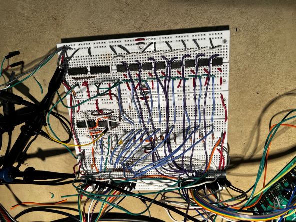
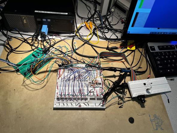
The work around that we devised consists of eight 23LC1024 SRAM and a few logic ICs. The implementation of our solution can be split into three sections: setting up our pins and configuring the target device (Initialization), reading data from the target and storing it in the SRAM (Target to SRAM), and reading the data from the SRAM and sending it to connected PC (SRAM to PC). At a high level, Target to SRAM works by sending a write instruction to the SRAMs, telling the target to transmit data, and then connecting each of the eight data lines from the target to the eight SRAMs in parallel. Once a full payload (in this case an image) has been received from the target, we begin SRAM to PC by giving the SRAMs a read instruction and then serially transmitting the data to the PC byte by byte. This solution enables us to read data into the SRAMs at the target frequency with little software intervention, and then retreive the data at our leisuire.
The SRAM module we chose communicates using the SPI protocal which requires four significant communication lines: chip select, clock line, data input, data output. For reference, here is a snippet from the SRAM Dataheet:
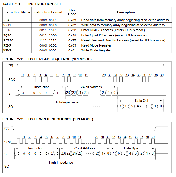
There are several instructions that the SRAM is capable of ingesting--the only two that are relevant to us are the READ and WRITE instructions. Both of these begin by dropping the active-low chip chip select (CS) for the entirety of the transaction. During the transaction, the clock line (SCK) pulses $32+n$ times, where $n$ is the number of data bits being written or read. The first 32 bits comprise the 8-bit instruction followed by a 24-bit address. The following $n$ bits correspond to a payload. In WRITE, the data input (MOSI) is read at the rising edge of SCK. Similarly, new data is written to the data output (MISO) at the rising edge of SCK in READ. Note that when $n>8$ (i.e. SCK is pulsed more than 8 times following the 32-bit instruction and address), the 23LC2024 enters sequential read or write mode (SEQREAD,SEQWRITE) which continues the respective operation by shifting the memory address by one every eight pulses until the CS is raised.
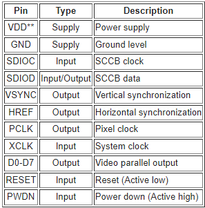
The OV7670, known hereinafter as the target, has the following pins:
The camera has several registers that can be configured to change the functionality of the device (a full list can be perused from the OV7670 Datasheet, although you may find more enjoyment in watching paint dry). We can write to these registers using the SCCB protocal over the SDIOC and SDIOD lines. An SCCB WRITE transaction is performed in accordance with the following snapshot from a logic analyizer:
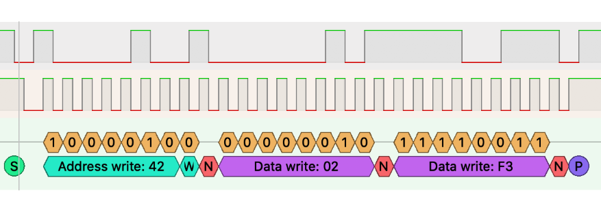
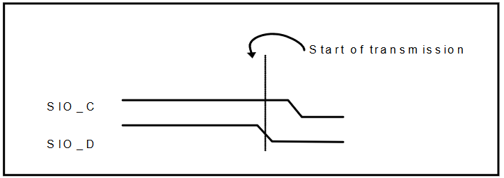
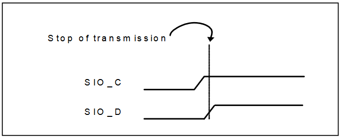
where S and P refer to the following start and stop sequences respectfully:
Now that we understand how to configure the camera, let's look at how to get data from the target. First, a clock line of at least 10 MHz needs to be provided to XCLK, at which point the target will immediatly start providing data across the eight parallel data pins D[0:7]. The new data is synchronized with three digital signals: VSYNC, HREF, and PCLK. We can visualize the effect of the former two using the following timing diagram:
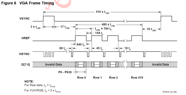
According to the datasheet, the falling edge of VSYNC indicates the start of a new image, and rising edge indicates its end. In contrast, the rising edge of HREF indicates the beginning of a new row of data, and the falling edge indicates that a row has ended. Note that the values of D[0:7] is meaningless at any instance that VSYNC is HIGH or HREF is LOW.
When it comes to actually extracting each byte, the datasheet provides us with a seperate diagram:
The latter signal used to synchronize the data is PCLK, a clock line provided by the target tied directly to XCLK. Similarly to the SRAM, new data becomes available at the rising edge of PCLK.
We manipulate our circuit using the following I/O pin header:
(pin of header, pin from PIC32, net label)
Pin 0:
- Ground
Pin 1:
- +3.3V
Pin 2:
- +5V
Pin 3, RPB3, SCS:
- PIC to SRAM chip select.
Pin 4, RPB13, CLK_SEL:
- Selects which clock pin is used.
Pin 5, RPB11, CAM_POW:
- Control pin for turning the camera on and off.
Pin 6, RPB7, FCLK:
- Output pin that sends out discrete pulses in order to emulate a clock. Used as SRAM clock while writing instruction.
Pin 7, RPB14, CCLK:
- 10 MHz square wave used the input clock to the camera module.
Pin 8, RPB8, SRAM_CMD:
- The MOSI line from the PIC to each of the SRAM modules used to transmit instructions.
Pin 9, RPB4, VSYNC:
- The VSYNC pin from the camera.
Pin 10-17, RPY0-7, Data Pins:
- Data out of the SRAMs connected to PORTY.
Pin 18, RPB1, SIO_DAT:
- The data line of the SCCB interface.
Pin 19, RPB2, SIO_CLK:
- The clock line of the SCCB interface.
We begin by initializing each of the I/O pins described above. An important note is that we drive the XCLK input of the target with CCLK, which is configured to leverage an output compare module and outputs a 10 MHz Square Wave.
Next, we configure the target by writing to the camera's internal registers using the SCCB protocal. Let $\phi$ be a function defined by $$\phi(reg, val):\text{write new value $val$ to register $reg$}.$$
The notable portions of our configuration include:
To see our exact configuration, take a look at ov7670.c
As we mentioned before, the goal is to feed the data from the target straight into the SRAMs without CPU intervention. To accomplish our goal, we need to hack the SPI transaction to allow the PIC32 to initialize a WRITE transaction (P1), and then give control to the target device so it can finish the data write (P2). More specifically,
VSYNC drops from HIGH to LOW indicating the start of a new image.VSYNC raises from LOW to HIGH indicating the end of the image.Here is some pseudocode to better understand each phase and the order of operations:
// ===== P1 START ===== \\

// drop chip select
mPORTBClearBits(SCS);

// send write instruction and address to SRAM
SRAM_Send(RAM_WRITE_CMD | addr);

// ===== P1   END ===== //

// turn on the camera
mPORTBClearBits(CAM_POW);

// wait for current image to end (VSYNC to go HIGH)
while (~mPORTBReadBits(VSYNC) & VSYNC);

// when VSYNC is HIGH, set clock select HIGH to indicate data is coming
mPORTBSetBits(CLK_SEL);

// wait for start of a new image (VSYNC to go back LOW)
while (mPORTBReadBits(VSYNC) & VSYNC);

// ===== P2 START ===== //

// raise chip select (VSYNC CS control takes over)
mPORTBSetBits(SCS);

// wait for the current image to end (VSYNC to go back HIGH)
while (~mPORTBReadBits(VSYNC) & VSYNC);

// ===== P2  END ===== //

// turn off the camera
mPORTBSetBits(CAM_POW);

// drop clock select
mPORTBClearBits(CLK_SEL);
These changes that we make in software result in the following phase-dependent hardware connections:
| SRAM Pin | P1 | P2 |
|---|---|---|
CS |
SCS |
independent of SCS |
SCK |
FCLK |
PCLK |
MOSI |
SRAM_CMD |
D[0:7] |
MISO |
PORTY[0:7] |
PORTY[0:7] |
To understand why we made these choices and why this works, we will seperate each of the four connections (except for MISO since we don't READ in this section) into their own subsections.
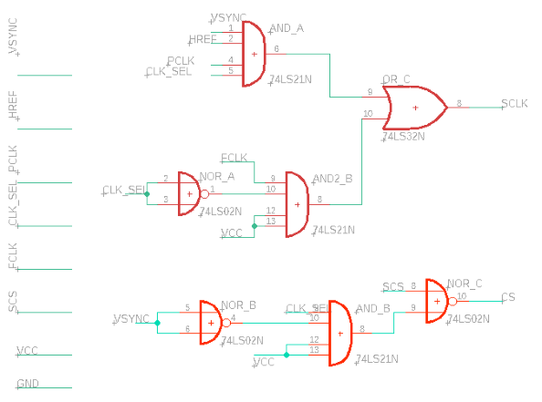
Here is a schematic of the logic we implemented for the chip select portion of the circuit:
In closed form, we can express the value of CS as
\begin{align*}
\mathrm{CS} & =\overline{\left( \left( \mathrm{CLK\_SEL} \cap \overline{\mathrm{VSYNC}} \right) \cup \overline{\mathrm{SCS}} \right)} \\
& =\overline{\left( \mathrm{CLK\_SEL}\cap\overline{\mathrm{VSYNC}} \right)} \cap \mathrm{SCS} \\
& =\left( \overline{\mathrm{CLK\_SEL}} \cup \mathrm{VSYNC} \right) \cap \mathrm{SCS} \\
& =A \cap \mathrm{SCS}.
\end{align*}
When we start P1, we drop SCS which causes CS to be LOW regardless of the values of CLK_SEL and VSYNC. At the moment P2 starts, CLK_SEL is HIGH, VSYNC is LOW, and SCS is set LOW. This causes A to be LOW, and thus, CS remains LOW. As soon as we finish P2, VSYNC goes HIGH which causes A to go HIGH, and thus, CS to go HIGH. Therefore, CS remains LOW for the entirety of the transaction and performs as expected.
def f1(CLK_SEL, VSYNC, SCS):
    return not ((CLK_SEL and not VSYNC) or not SCS)

def f2(CLK_SEL, VSYNC, SCS):
    return not (CLK_SEL and not VSYNC) and SCS

def f3(CLK_SEL, VSYNC, SCS):
    return (not CLK_SEL or VSYNC) and SCS

for CLK_SEL in range(2):
    for VSYNC in range(2):
        for SCS in range(2):
            v1 = f1(CLK_SEL, VSYNC, SCS)
            v2 = f2(CLK_SEL, VSYNC, SCS)
            v3 = f3(CLK_SEL, VSYNC, SCS)

            assert v1 == v2 == v3
            # print((CLK_SEL, VSYNC, SCS), v1 == v2 == v3)
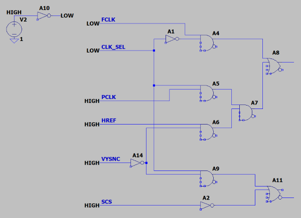
Here is a schematic of the logic we implemented for the clock line:
In closed form, we can express the value of SCK as
\begin{align*}
\mathrm{SCK} & =\left( \mathrm{FCLK} \cap \overline{\mathrm{CLK\_SEL}} \right) \cup \left( \mathrm{PCLK} \cap \mathrm{CLK\_SEL} \cap \mathrm{HREF} \cap \overline{\mathrm{VSYNC}} \right) \\
& =A \cap B.
\end{align*}
During P1, we want the SRAM to be in phase with FCLK, which is a bit-banged output signal which we use as the clock while writing the instruction and address. On the other hand, we want the SRAM to be in phase with PCLK during P2 because the data is output from the target at the rising edge of PCLK.
From the pseudocode, we can see that CLK_SEL is LOW during P1 which causes B to go LOW and for the output signal of the OR gate to pulse in phase with FCLK. Thus, SCLK is set correctly for P1. For P2, CLK_SEL is HIGH which causes A to go LOW and B to be in phase with HREF and PCLK (note that this is the only time we want data loaded into the SRAM). Therefore, SCK is set correctly for both phases.
Here is a schematic of the logic we implemented for the clock line:
In closed form, we can represent MOSI as
\begin{align*}
\mathrm{MOSI}_i & =\mathrm{SRAM\_CMD}\times\mathrm{FCLK} + \mathrm{D}_i\times\mathrm{PCLK},
\end{align*}
where MOSI_i represents the $i$-th SRAM and D_i represents the $i$-th data line from the target.
In this configuration, each of the SRAMs have a shared line from the PIC32 which is used to transmit the instruction. During P1, we set the PWDN pin of the target HIGH which causes the camera to go in standby mode, during which PCLK does not pulse and D[0:7] is LOW. Thus, $\mathrm{MOSI}_i=\mathrm{SRAM\_CMD}$ whenever FCLK pulses during P1. During P2, however, FCLK is always LOW, and thus, $\mathrm{MOSI}_i=\mathrm{D}_i$ whenever PCLK pulses. Note also that the diodes protect each of the outputs, and the pulldown resistor ensures that MOSI never floats. Therefore, the MOSI lines are set correctly for both phases.
With the data from the camera stored in the SRAM modules, it is then streamed through the PIC to the PC. This begins with an SPI transaction between the SRAM and PIC. The SRAM remains in phase with FCLK for this entire transaction. The first few rows of the camera data saved to the SRAM does not contain useful image data and is discarded. The actual image data is then read by pulsing FCLK high, then reading each byte with readPE(GPIOY), then setting FCLK low again.
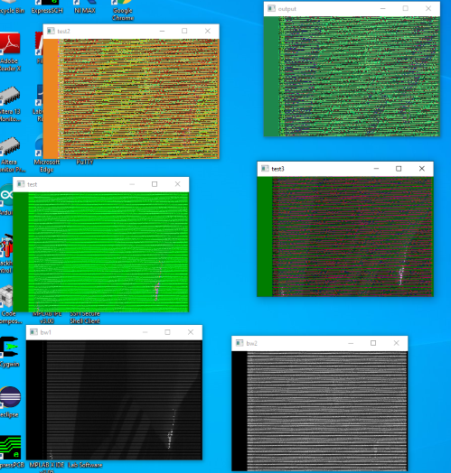
Each byte read from the SRAM with readPE(GPIOY) is sent to the PC over UART using printf("%c", readPE(GPIOY)); between the clock pulses. This data can then be picked up by by a python script and displayed. The results from this can be seen below.
There are a few major points that we want to verify from our image output:
As we stated before, the OV7670 has several color formats for which it will output--we chose YUV. Based on the YUV and CIF register configuration, the camera should output $352\times240\times2$ bytes of data in the following order:
| Byte 0 | Byte 1 | Byte 2 | Byte 3 | Byte 4 | Byte 5 | ... | Byte 168,958 | Byte 168,959 | |
|---|---|---|---|---|---|---|---|---|---|
| Data | $Y_0$ | $U_0$ | $Y_1$ | $V_1$ | $Y_2$ | $U_2$ | ... | $Y_{84479}$ | $V_{84478}$ |
Each of the $P_0,...,P_i,...,P_{84479}$ pixels have their own luminence $Y_i$, but pixels $P_i,P_{i+1}$ share chroma components $U_i,V_i$ for each $i$ s.t. $i\mod 2=0$. In other words, each pixel can be stroed using an average of 2 bytes by arranging them as
| Pixel | YUV Encoding |
|---|---|
| Pixel 0 | $Y_0~U_0~V_0$ |
| Pixel 1 | $Y_1~U_0~V_0$ |
| Pixel 2 | $Y_2~U_2~V_2$ |
| ... | ... |
In order to convert a YUV image to RGB, we create a pixel $[R_i,G_i,B_i]$ for each $P_i$, where $R_i,G_i,B_i$ are obtained by \begin{align*} R_i & =Y_i + 1.402\times\left( U_{(i-i\mod2)} - 128 \right), \\ G_i & =Y_i + 0.34414\times\left( V_{(i-i\mod2)} - 128 \right) - 0.71414\times\left( U_{(i-i\mod2)} - 128 \right),\text{ and} \\ B_i &=Y_i + 1.772\times\left( V_{(i-i\mod2)} - 128 \right). \end{align*}
If we were to compare the RGB output with images simply encoded with only $Y$ values, only $U$ values, and only $V$, we would observe the following:

Clearly the $Y$ channel encodes the gray scale portion of the image while the $U$ and $V$ encode the colors.
After reading data from the camera and storing it across eight parallel SRAMs, the PIC32 serially transmits the data to a Python script which converts the data to images. Below, we have six windows all showing the same image, but each window constructs the image using different YUV-to-RGB conversions.
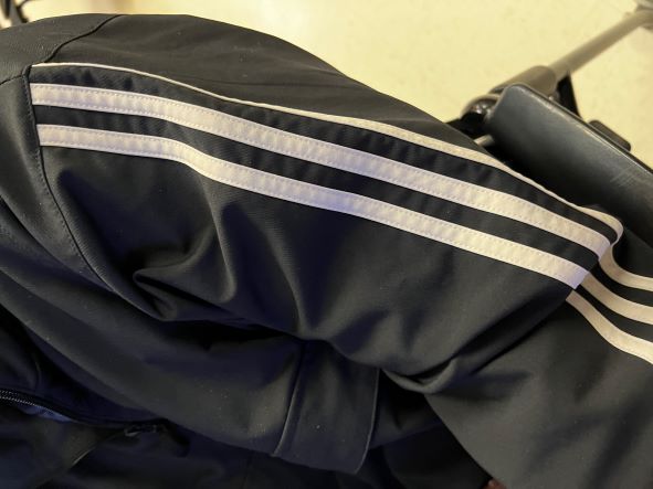
And here is the same subject but captured on an iPhone:
We constructed the bottom two images by taking each even byte $A$ and odd byte $B$ in our data stream and adding pixels $[A,A,A]$ and $[B,B,B]$ to images bw1 and bw2 respectively. Since bw1 is the gray scale representation of the image, we can confirm that the camera is sending the bytes in the correct order. The other four windows are each different attempts at converting the data to an RGB image. Although you can clearly make out the same shapes in the colored images as the B/W images, something is not correct. We have deduced that it's most likely an issue with the camera, and given more time to mess around with the configurations, a proper image could be resolved.
The import thing to note is that the pixels are aligned and we can definitevly state that the we received an image from the camera. This also shows that the data streamed into the SRAM from the camera is then read out from the SRAM in the correct order. By these metrics, we have proven that we can read data from a target device asynchronously using our parallel SRAM configuration. This is very applicable because our circuit effectively acts as a buffer to help high speed periphreals interact with low speed devices.
Below is a video from our final demo explaining how everything works.
In conclusion, the high bandwidth low latency communication with a target device was a success. Despite the poor camera quality, we were able to get an image from the camera to the PIC through the SRAM modules with little software intervention. This project involved a large amount of trouble shooting, which invovled several tools such as a function generator and an oscilloscope. These tools were largely used to deal with the timing requirements of our bit banged communication protocols. They were also used to ensure that data output from the target matched what we were reading from the SRAMs. If we were to continue this project, we would improve the camera quality, then add wireless communication so that the camera does not have to be connected to the computer to take a picture. If anything were to be changed, we would likely have used a different camera. Ultimately, we've shown that high bandwidth, high speed devices can be used without a high frequency CPU.
We were expecting higher image quality when we started. In fact, we expected the camera to be the easier part to deal with. In reality, the camera lacked documentation and the documentation available was not always accurate either. This made it difficult to figure out how to get a good image from this camera.
The group approves this report for inclusion on the course website.
The group approves the video for inclusion on the course youtube channel.
OV7670 camera: $8.99
Bluetooth module (unused but still bought): $12.99
Joseph Whelan: Software Development, Hardware Development, SRAM Documentation
Devlin Babcock: Software Development, OV7670/SCCB Documentation
Akugbe Imudia: Hardware Development, OV7670/SCCB Documentation