Hardware Details
Our hardware design is based around a 16Mhz Atmel ATmega32 processor on a STK-500 board with a sister ATmega163 sister MCU running on a 4Mhz STK-200 board. The two boards communicate to each other via PORTB on the STK-500 and PORTD on the STK-200. The overal schematic and the various Port Assignments are listed below:
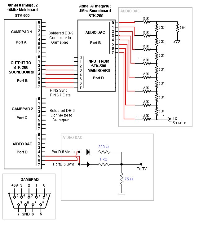
STK-500
Port Assignment
|
PORTA |
Sega Controller #1 |
|
PORTB |
Connection
to STK-200 for Audio |
|
PORTC |
Sega Controller #2 |
|
PORTD |
Video DAC |
*Ports
not listed are not assigned
STK-200 Port Assignment
|
PORTB |
Audio DAC |
|
PORTD |
Connection from STK-500 |
*Ports
not listed are not assigned
DACs
facilitates the conversion of our digital audio and video output to the analog
signal required by the TV. Two AV cables feeds our signal to the TV. (Video
– Yellow, Audio – White). The 2-bit DAC used for video output was based on
the design from lab 3. The Video DAC is connected to pin 5 and pin 6 of PORTD.
A 7-bit DAC, based on the design from lab 5, was used to facilitate the conversion from the digital output to the analog signal required. The Audio DAC is connected to all 8 pins of PORTD on the STK-200.
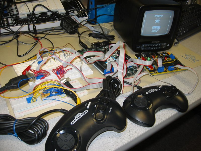
The Sega Controller was chosen as input device. This is because it has a serial (DC-9) interface which enables us to elegantly connect it to our board using female serial sockets. We initially wanted to use the Playstation or SNES controllers; however, unlike the Sega, they output their signals via a shift register; thus, we need to have a clock signal and a sequential polling scheme to read in the inputs. Given the time constraints of the TV, this is virtually impossible to do. Thus, we settled with the Sega.
The Sega Controllers used for user input has 6 buttons: Up, Down, Left, Right, A, B, C, Start. However, only B, C, or A, Start can be polled at any one time as they share the same output pin. The output pin can be switched between B,C and A,Start via a MUX selector PIN. However, in order to poll the controller after a MUX signal change, we must insert 3 nop functions in assembly so that the resistors have enough time to pullup to the correct voltage value. The 3 nop functions; however, will lead to jitter on the TV screen unless we split the task over 2 frames. Thus, since our game does not require too many buttons, we simply decided to use buttons B and C only. The Sega Controllers are connected to PORTA and PORTC. The wiring connections are identical and the pinout diagrams are shown below:
Sega Genesis Pin Layout
|
Diagram of
Pin Layout
|
Pin Settings
|
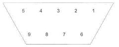 |
Pin
Select: low Select: high --- ------------ ------------ 1 joypad up joypad up 2 joypad down joypad down 3 logic low joypad left 4 logic low joypad right 6 button A button B 9 start button button C Pin Connection |
Things
That Did Not Work
Another obstacle came up when we connected Controller #2 to PORTB. When we connected the circuit this way, the chip failed to program properly. After removing the Controller from PORTB, the chip programmed perfectly. Then, we realized that PORTB was the programming port, and when we use it as an input, the input signals from the controller would interfere with that from the serial port; thus, we were not able to program the chip. Therefore, we modified our code so that PORTC became the input port for Controller #2 and we used PORTB as an output to communicate with the STK-200 sound board. After this modification, our hardware setup functioned properly
As our code grew, we started to run out of memory. We encountered the error “out of memory for global variables” quite early on. This error was due to the fact that I declared two arrays, board[10][10] and score[10][10] as int variables. As int variables are 16-bits, they require considerably more memory than char variables. After changing board[][] and score[][] to char, the memory problem was solved. I have also moved all of the strings to the flash memory in order to free up space for variables.
Another
error which we encountered was instability of the communication signal between
the STK-500 and the STK-200 soundboard. Whenever we need the soundboard to
play a song, we need to send a command signal on PORTB.3 to PORTB.7 to indicate
the song. Then, we need to send a square wave pulse on PORTB.2 so that it
will activate the ISR on the Mega163. However, we found that by simply using
PORTB.2=1 followed by PORTB.2=0 leads to very unstable results. The soundboard
often ignores the command from the STK-500. We believe that this is due to
the fact that the STK-500 is running at a much higher frequency than the STK-200
(16Mhz vs. 4Mhz.). Thus, the square wave was too short to be detected by the
Mega163 which is running at 4Mhz. Thus, we lengthened the square pulse by
putting codes between the PORTB.2=1 and PORTB.2=0 command. Then, the sounds
played perfectly.