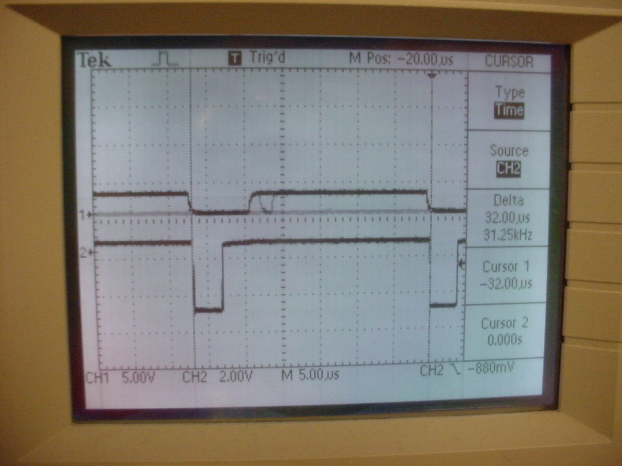
Figure 1: Oscilloscope demonstrating hsync signal generation on channel 2. Channel 1 displays an "all red" signal.
by Ameya Agaskar (apa22) and Aaron Kimball (ak333)
Wednesday 1:30pm lab
A system consisting of an ATMEL MEGA32 chip, Altera FLEX10K FPGA, and a library of source code for the Atmel processor to generate 256-color VGA video signals in real time optimized for game development.
The Nintendo Entertainment System sports 2 KB of RAM and a 1.79 MHz 8-bit processor. Using an additional video processing chip, it is capable of displaying 48 colors (16 simultaneously) at a resolution of 256 by 224 pixels. Knowing the technical limitations of the system, we felt that an ATMEL microprocessor with some additional hardware to handle the video bandwidth would be capable of reproducing a similar game programming environment for amateur game hackers.
To distinguish our project from previous ECE 476 final projects, we chose to generate VGA output instead of the NTSC iamges favored by previous designs. While time constraints prevented us from generating a full-scale game, we have succeeded in creating a game development environment with all of the "dirty work" done. Our project features custom hardware running on an Altera Flex10K FPGA which generates VGA video in 256 colors at a resolution of 200x160 pixels, and stores the neccessary screen buffer data in its RAM. A communications protocol we developed allows an ATMEL microprocessor to control the screen's contents by downloading a tile map and tile descriptions to the FPGA during the screen blanking period. Additional control logic allows freely positioned "sprites" to be displayed on top of this tiled background. Finally, some simple code enables a would-be game to utilize an NES or Super NES controller for user input.
Our system is composed of one Atmel MEGA32 processor running on an STK500 development board, an Altera Flex10K FPGA on a UP2 development board, and an array of DACs implemented by hand on a whiteboard. The FPGA is used to store screen data and drive the VGA signal (generating horizontal and vertical sync signals using its internal clock, and sending digital color information to the DACs for the analog VGA lines). The screen is abstracted as a two-dimensional array of 8 pixel by 8 pixel "tiles" -- indices into an array of 8x8 bitmaps consisting of 8 bits of color information per pixel. The FPGA is directed in what data to display by the Atmel processor which maintains a computer game or other application's state. The Atmel downloads tile bitmaps and screen tile arrays to the FPGA using a communication protocol described in the appendix. Timing is synchronized by using external interrupts generated by the FPGA coincident with line and screen blanking periods. The Atmel processor can also communicate with an external game controller over an additional I/O port.
The main standard encountered by this project will be the VGA signal standard. We successfully implemented this standard, and tested our system with a regular VGA monitor.
We utilized an Altera Flex10K FPGA to implement the screen buffer and to generate the VGA output. The FPGA has 18 kilobits of RAM. Three RAM blocks are instantiated: a tile definition block, a sprite definition block, and a screen buffer block.
Each tile and sprite is an 8 pixel by 8 pixel block. Each pixel contains an 8-bit color value: 3 bits of red, 3 bits of green, and 2 bits of blue. The tile RAM can store up to 16 tiles. The sprite RAM can store up to 4 sprites.
The screen is 200 pixels wide by 160 pixels high. The screen buffer is 26 tiles wide by 20 tiles tall. Each position in the screen RAM stores an index into the tile memory. The extra column is used in scrolling. The FPGA stores a horizontal offset value between 0 and 7. The entire screen is shifted this number of pixels to the left, with pixels on the right side being pulled from the 26th column of tiles as neccessary. This horizontal offset is incremented by one on a positive edge of the "scroll" signal from the ATMEL, and is reset to zero when the "reset_X_off" signal goes high.
The VGA standard uses 5 lines: a horizontal sync, a vertical sync, and analog red, green, and blue signals. The FPGA is conveniently clocked at 25.175MHz, which is the pixel rate for the VGA signal. The FPGA uses a counter clocked at this rate to count "logical pixels." The horizontal blanking, sync, and active video portions of each line are generated based on this counter. A vertical counter is clocked using "logical lines." The vertical blanking, sync, and active video portions of each frame are generated based on this counter. Since the RAMs on the FPGA are single-port RAMS, the VGA module turns off the write enable signal for the RAMs when they need to be read to determine the pixel value to be output. The VGA module uses the current row and column number to generate an index into the screen buffer RAM, whose output is an index into the tile definition RAM. Meanwhile, the ATMEL can specify the position of up to two sprites. These positions are used to generate an index into the sprite definition RAM. Based on the current row and column, the output from the tile definition RAM and the sprite definition RAM is MUXed to generate the pixel output.
We use three DACs (of 3, 3, and 2 bits each) to generate the analog red, green, and blue signals sent to the VGA monitor. The VGA standard calls for values ranging from 0.0V to 0.7V for each wire, with 0.7V yielding the highest intensity, and 0.0V indicating black. The input impedence for each of these signals is 75 Ohms. We implemented the DACs using an R-2R ladder design, built on banks of matched 10KOhm resistors. The 10 KOhm resistors keep the actual current draw from the FPGA low, but do not possess enough power to actually drive VGA signals. Therefore, we used 3 fast op-amps (TI OPA37GP's) in voltage-follower configurations to isolate the signal generation from the signal delivery. Since the DAC output ranges from 0-5V, we used a 330 Ohm resistor after each op amp to voltage divide the signals down to 0.7V maximum. The op-amps draw their power from a separate power supply with +/-12V rails.
Our ATMEL can also interface with an NES or Super NES game controller for user input. Each of these controllers internally uses a standard 4021 8-bit linear shift register chip. When the "latch" line is pulsed, the state of all buttons on the controller is recorded into the shift register. Pulses on the "clock" line then advance the output of the shift register, sending a 1 or a 0 on the "data" line back to the ATMEL chip for each of the 8 buttons (including the 4-way directional pad) in a predetermined order.
Our initial design called for a 64 KB SRAM to be used as a full screen buffer. Buying a dual-port SRAM would enable an address generator to generate the VGA output signal from the screen buffer, while the ATMEL chip could fill the screen buffer from the other port. This plan was abandoned when we realized that 64 KB SRAM chips were only available in surface-mount and other difficult-to-solder configurations.
The ATMEL software consists of a library of functions designed around the shared communications protocol. We include functions for downloading tile and sprite bitmaps to the FPGA. Other functions quickly set the sprites for the current screen row, and strobe a full screen or column of tiles to the FPGA. (Individual tiles can also be set with another function.) A separate function will quickly read in the game controller state for use.
The FPGA generates two falling-edge signals corresponding to the beginning of horizontal and vertical blanking. The ATMEL interprets these as external interrupts and invokes two interrupt handlers, which currently count which logical screen line the FPGA is displaying.
Our main program initializes the ATMEL's ports and interrupts, downloads the tile images to the FPGA RAM, and then enters the main loop. In the loop, it fills the screen with an image reading "ECE 476!". At every vblank period, it commands the FPGA to scroll left by 1 pixel. Every eighth scroll, it downloads the entire screen again, but advanced by a single column of tiles. The result is a demo screen which wraps the "ECE 476!" message horizontally.
The ATMEL code is also responsible for storing the tile maps for game levels, as well as the tile and sprite bitmaps in its flash RAM. Since the FPGA clears on boot, the ATMEL must re-download its tiles to the FPGA at game start. This design also allows increased flexibility, as different tiles could be loaded in at different points of a game to allow a much wider variety of game environments within a single program.
While this proof-of-concept program only does the above, it is the framework upon which a more complicated program such as a game could be written. The major modification would be performing game update logic in the vertical blanking period. (Downloading a full screen of tiles to the FPGA requires approximately 7,600 cycles of the ATMEL's processor, which must be done once per eight scrolls. The vertical blanking period is approximately 22,800 cycles, yielding ample time for additional processing.)
Nearly all I/O pins on the ATMEL are used. Interfacing with a video game controller requires 3 pins on port D. Two other pins on port D trigger the line- and frame-end interrupts. Ports A, B, C, and 3 pins of port D are all used as output to the FPGA for one-way communication purposes. The entire protocol is listed in the appendix.
Throughout the process, the software code was remarkably easy to write, given the nature of the task. The major difficulties in our project lay in building the hardware device itself; through careful design we were able to avoid most problems in advance.
Our system works as described. Continuous scrolling is some times (approximately one pixel in 40) jerky, resulting in an annoying but negligible "click" in the scroll process. The DAC and op-amp circuit also seems to lack the bandwidth to handle sudden changes in brightness. As a result, a solid block of one color followed by a solid block of another color will cause the first one to "bleed" into the second for a few pixels. While this is regrettable, a single-chip DAC circuit would probably alleviate these issues. At the time we were doing our design, we dismissed this option for cost reasons. Since we are under budget, a "future rev" of this project would most likely include a higher-performance integrated DAC circuit.
One additional issue is that writes to the tile bitmap memory did not always seem to succeed on the first try; we cannot find a reason for the values to fail to take hold, since the same data lines succeed in writing to the screen buffer memory every time. Our work-around solution is to send each value from the Atmel to the FPGA multiple times. While technically "non-deterministic," it has proven to be a reliable mechanism. Future revisions of this system would focus on increasing data transfer reliability.
We tested the timing of the VGA sync signal generation. We generate horizontal sync pulses with accuracy within 25 us of the target time for a line. Vertical sync pulses are generated with a period of 16.70 ms; this is very close to the 16.68ms standard, and is accepted by our test monitor.
Figure 1: Oscilloscope demonstrating hsync signal generation on
channel 2. Channel 1 displays an "all red" signal.
Below are screen captures from the VGA monitor.
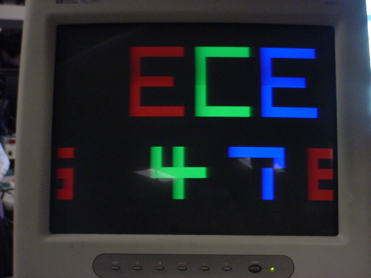
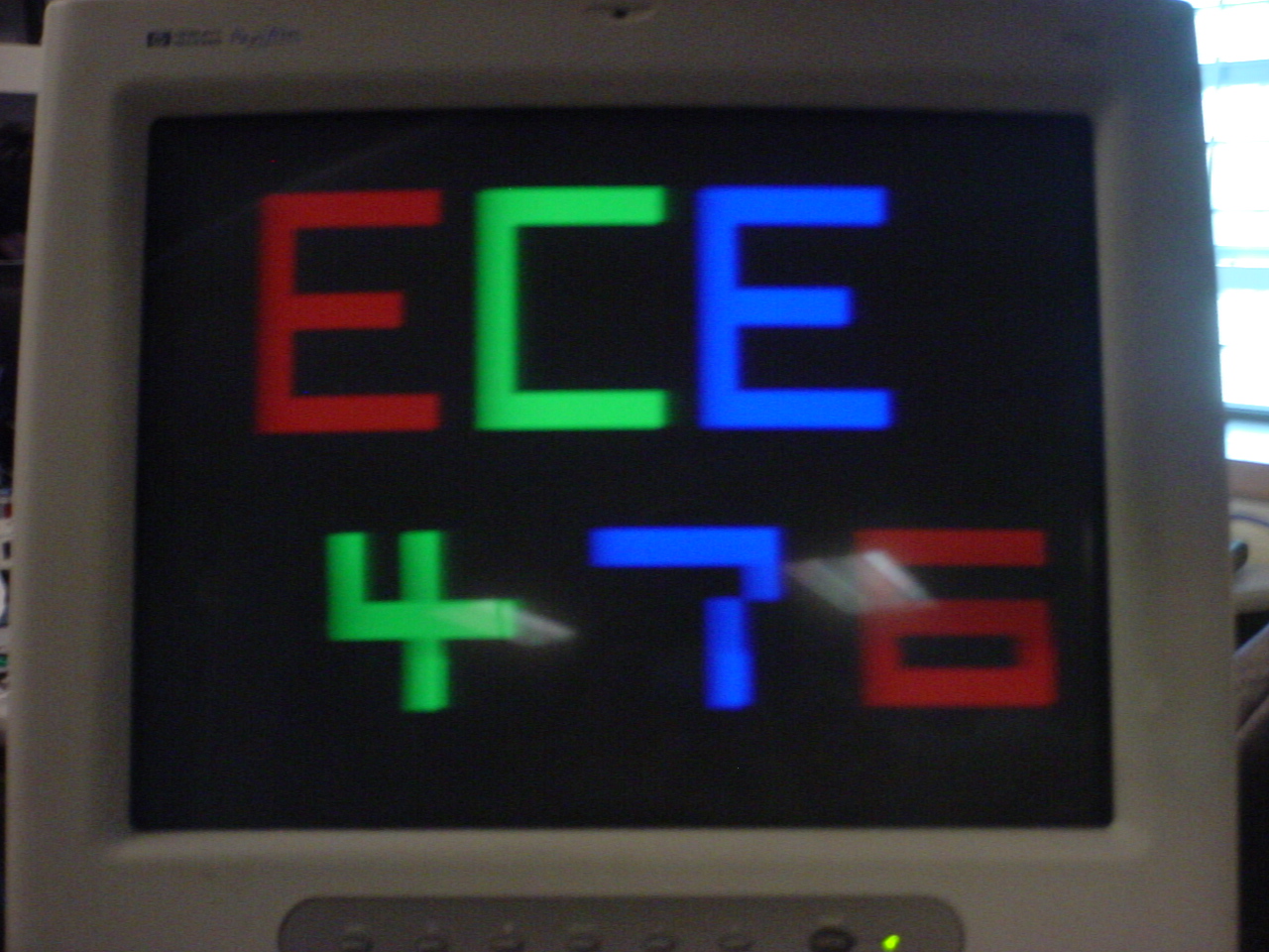
Figure 2: Screen captures illustrating scrolling
Video demonstrating scrolling image (MPG, approx. 800 KB)
Safety Information
Our project is safe for use by virtually anyone. While in its current form, it is vulnerable to electrostatic shock, this could be solved by careful packaging. It does not generate large electrical currents, nor does it involve the use of any motors or other potentially dangerous parts. To be extra safe, we heat-shrinked the wiring connected to the external VGA header.
Usability
In the hands of a competant Atmel programmer, this represents a very viable platform for future game creation. Connecting the various boards is a simple process now that the internal wiring is done; users of this kit could see VGA output in a matter of a few minutes. Developing a game, while a complicated process, would be no more difficult using this system than the sample source code given for lab 4.
We are excited about our successful project effort. While we did not achieve our "reach" goal of actually creating a game to operate on top of our platform, we still feel that we accomplished the bulk of the work. With additional lab time available, such a game could be realized. The main factor in this goal modification is that we underestimated the amount of time required to actually implement the physical devices such as the DAC and another wiring. Both the ATMEL and FPGA designs worked remarkably well with relatively little debugging; the bulk of our debugging time was spent on physical issues such as impedence matching and wiring.
Standards
We adhered to all relevant standards, which include the VGA output standard, and the protocol for communicating with the 4021 chip in a game controller (described in the 4021 datasheet -- see appendix). True VGA timing calls for a 3.77 us horizontal sync period. Due to the frequency of the FLEX10K's clock, the closest we could generate to this period is 4 us. This has proven to work with our test monitor; since all other timing is very accurate, we stay within .2% of the overall timing specification.
Intellectual Property Concerns
To our knowledge, there are no IP concerns in the development of this project. We created all source code and hardware definition code from scratch for our implementation. We hereby grant an unrestricted license for academic, non-commercial use of our source code in any derivative game projects. One concern may be that Ameya Agaskar has developed a VGA output device in Verilog before, under employment by the Sarnoff corporation. While he has a non-disclosure agreement with Sarnoff, we believe that this does not cover his knowledge of VGA implementations. As the VGA specification is an open standard, developing a VGA driver does not constitute a trade secret of Sarnoff. Furthermore, we did not copy any code used in Ameya's project for Sarnoff -- we redeveloped the VGA driver from scratch, and implemented the internals in a different way that fit the tiling system and other unique constraints of our design.
Ethical Considerations
Referring to the IEEE code of ethics, we have followed the rules below.
1. to accept responsibility in making engineering decisions consistent with the safety, health and welfare of the public, and to disclose promptly factors that might endanger the public or the environment;
To our knowledge, our device is safe for the public. Little risk is incurred by users of our hardware. Since we have adhered to the published specifications for interoperability between our device and VGA monitors, we do not believe we could damage a VGA monitor with our system.
2. to avoid real or perceived conflicts of interest whenever possible, and to disclose them to affected parties when they do exist;
We do not believe we have created a conflict of interest with our system. We address a potential intellectual property collision in our IP concerns section above; while we do not believe there is a conflict of interest, we would pursue an agreement with Sarnoff absolving them of any claim to our device if we were to commercially distribute this package.
3. to be honest and realistic in stating claims or estimates based on available data;
Our report accurately describes the state of our system.
4. to reject bribery in all its forms;
Nobody offered any bribes to us during the course of this project. Since there is no ground for us to accept any bribe, we would not do so anyway. Our primary concern is a high grade on this project, which we hope we have achieved through our hard work.
5. to improve the understanding of technology, its appropriate application, and potential consequences;
We improved our own understanding of VGA standards and microcontroller programming. Having destroyed microchips in the past, we were well aware of the consequences of faulty wiring and design. We took great pains to ensure that we did not try to draw too much current through any device or damage any of the equipment we were using.
6. to maintain and improve our technical competence and to undertake technological tasks for others only if qualified by training or experience, or after full disclosure of pertinent limitations;
We have learned a lot over the course of this design project. We believe that our technical competence has improved throughout this experience. We feel that we had adequate training to begin this design project after successfully completing all five labs in ECE 476 to the instructor's satisfaction.
7. to seek, accept, and offer honest criticism of technical work, to acknowledge and correct errors, and to credit properly the contributions of others;
We believe that we have supplied attribution to all other parties who assisted us in this project development, and cited all sources of knowledge and specifications. Throughout ECE 476, we have accepted criticism in the context of our Lab TA's feedback on our projects, and continued to do so throughout the design project. Though no other students had particular criticism of our efforts, we would have accepted this as well.
8. to treat fairly all persons regardless of such factors as race, religion, gender, disability, age, or national origin;
No discrimination took place in the development of this project.
9. to avoid injuring others, their property, reputation, or employment by false or malicious action;
We did not harm anyone, nor did we break any equipment in the design and implementation of this project.
10. to assist colleagues and co-workers in their professional development and to support them in following this code of ethics.
We have always strived to follow the IEEE code of ethics and the Cornell University code of Academic Integrity. If in the course of this class, we were to see anyone violating these policies, we would have alerted the course staff or the professor. Fortunately, this was never an issue.
Future work
We would like to thank Professor Land and our Lab TA Richard West for the opportunity to make this project. An additional hearty thank-you goes to Dr. Swartz of the ECE department, who graciously allowed us to use one of his FPGA development boards, and even soldered a large pin-header directly onto the FPGA development board for us to use.
Atmel
Altera
Texas Instruments
Altera UP2 Dev board datasheet
Atmel MEGA32 datasheet
4021 shift register datasheet
NES controller pinout
VGA Timing information (Warning: semi-annoying ads)
VGA connector pinout
Download FPGA VGA Driver implementation (Verilog)
Download Game platform implementation (ATMEL C)
Display of colors available for generation (approximate)
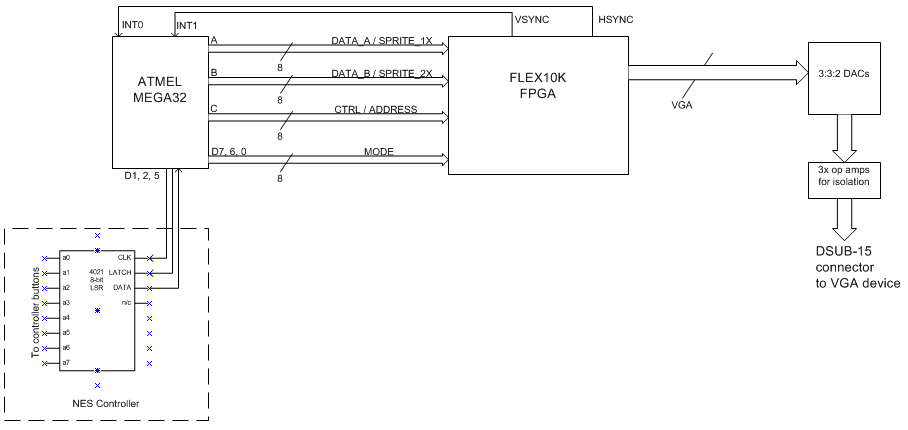
Figure 3: block diagram
Project budget:
| ATMEL Mega32 chip | $8 | "rental" |
| ATMEL STK500 | $15 | "rental" |
| VGA Monitor | free | (Aaron's) |
| SNES controller | free | (Ameya's) |
| ALTERA UP2 & FLEX10K | free | scrounged -- obsolete ECE 230 hardware |
| VGA female connector (DB-15 connector) | $2.00 | Radio Shack |
| Test 4021 chip | $0.48 | DigiKey |
| 3 x OPA37GP op amps | free | Sampled - Texas Instruments |
| 4 x matched 10 KOhm resistor packs | free | in-lab components |
| 12V power supply | $5 | "rental" |
| whiteboard | $6 | "rental" |
| Total: | $36.48 |
Labor breakdown:
Communications protocol:
PORT A

A.7-A.0 : DATA                          In download tile and download sprite modes,
                                        contains pixel value for selected address and
                                        tile/sprite.

A.4-A.0 : X_COORD                       In set tilemap mode, contains x-coordinate (0-24)
                                        of entry in tilemap to set

A.7-A.0 : SPRITE1_X                     During video output, the x-coordinate of
                                        sprite 1.


------------------------------------------------------------------------------------------

PORT B


B.3-B.0 : TILE_NUM_TO_DL                Which tile entry (0-15) to write to
                                        during tile download operation.

B.1-B.0 : SPRITE NUMBER                 Which sprite entry (0-3) to write to
                                        during tile download operation

B.4-B.0 : Y_COORD                       In set tilemap mode, contains y-coordinate (0-20)
                                        of entry in tilemap to set.

B.7-B.0 : SPRITE2_X                     During video output, the x-coordinate of
                                        sprite 2.

------------------------------------------------------------------------------------------

PORT C

C.7 : SCROLL                            If high, current line should be scrolled
                                        one pixel right-to-left. (Will be set
                                        before beginning of line draw, and will
                                        hold through til next HSYNC.)

C.6: RESET_XOFF                         On pos edge, the "X offset" should be
                                        forced back to 0, regardless of where
                                        the scrolling process currently is.
                                        (Async signal)

C.5-C.0 : ADDRESS                       In tile or sprite download mode, address to
                                        the pixel within the tile/sprite whose
                                        value should be changed.

C.3-C.0 : TILE_NUM_TO_OUTPUT            In set tilemap mode, sets which tile number
                                        place in the specified X and Y position.

C.3-C.2 : SPRITE2_NUM                   Identity of sprite 2.
C.1-C.0 : SPRITE1_NUM                   Identity of sprite 1.

-------------------------------------------------------------------------------------------

PORT D

D.7-D.6 : MODE                          00 - no action
                                        01 - download tile
                                        10 - download sprite
                                        11 - set tilemap

D.0 : DATA CLOCK                        Goes positive when all values in a coordinated
                                        transfer are ready.