Our one sentence "sound byte"... *POP*
Finally, a fair and balanced way to score Tae Kwon Do matches without the moaning and groaning of everyone. The Electronic Hogu system uses piezoelectric force sensors to determine how much force is delivered by the impact of a strike. Using waveform analysis and analog-digital conversion, it is possible to create constraints to determine what truly should and should not score in a match. By driving a CRT monitor with the STK500's PWM, we can also have a score display to tell how many points a player has. Most importantly, wireless communication via OOK (On-Off Keying) between the hogu and the base station is integral to the effectiveness of this system as it provides a fast and easy way to transfer information quickly without a tethered system. Ultimately, our system makes much needed improvements to an age-old game by taking traditional martial arts into the future.
The inspiration for this project came from Kevin's own interest in TKD and our collective interest in the way that it implemented a collection of previous labs to reach a common goal. The fact that it was possible to implement this project could be considered either a well-timed coincidence or destiny. Either way, it was interesting to see that a commercially produced product sold at astronomical prices, nearly $3000 for a system[1], could be manufactured with individual parts for a much smaller fee.
Before the advent of electronic hogus, two Tae Kwon Do opponents would spar and three corner judges would observe the match and award a point to the fighter who landed a hit on the other; however in instances where the opponents attack nearly simultaneously it is difficult for the judge to correctly reward the deserving opponent. If two electronic hogus are hit milliseconds apart, the difference can be discerned electronically and the fighter who struck first will be given a point. We viewed a YouTube video[2] demonstrating the wireless electronic hogus and we decided to design and implement our own hogu using knowledge obtained in ECE476 throughout the semester.
The logical structure of our design is two have two main components: the transmitter side and the receiver side. The transmitter side consists of the hogu implanted with piezoelectric sensors, an MCU implementing a hit detection scheme, and wireless transmission circuitry that sends a specific byte of data when a hit is detected. The receiver side consists of wireless receiver circuitry, an MCU that waits until the specific byte is received, and a TV to keep track of score and penalties. Detailed descriptions of the two sides can be found in section 3.2.
Throughout the project it was clear when to use hardware and when to use software. The only time in which we considered both hardware and software to achieve the same goal was to discern between hardware filtering versus digital filtering. We first tried to implement the filter in software to save soldering time but were met with problems with signal attenuation; therefore we resorted to making a hardware filter which we found was ultimately easier to test and debug.
Our design does not relate to any known standards; however the wireless protocol that we use was developed by Meghan Desai so the FCC legal restrictions must be taken into account. Further discussion of the FCC legal restrictions can be found in section 5.4. Our overall design is a reasonable reconstruction of a potential system as hinted at by one of our supporters, Jin Song.
Electronic hogus are developed commercially so exist various patents, copyrights and trademarks with varying companies. When sampling the piezoelectric sensors we were required to sign a non-disclosure agreement with CNOwire pledging not to market critical design elements to the public. The test hogu that was implanted with the sensors was manufactured by Adidas.
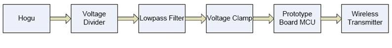
Figure 1 shows the high level schematic of the components involved at the transmitter side. Each component will ultimately be discussed in detail, but the general description of each component is as follows. The output voltage from the hogu is roughly 10V to 15V for a solid hit, but can go up to 20V or more for a very strong hit. Therefore a voltage divider is used to scale this voltage to a reasonable level. The lowpass filter is used to attenuate noise. The voltage clamp is a safety measure so that the pins of the MCU are not overloaded by a large voltage that might destroy the chip. A prototype board houses an MCU that analyzes whether the hogu has been hit hard enough to register as a hit. The MCU controls the wireless transmitter that will send data to the receiver at the lab station if a hit is detected.
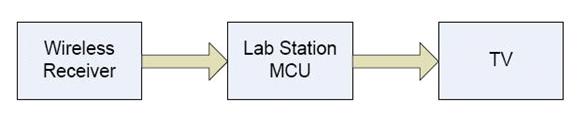
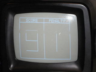
Figure 2 shows the high level schematic of the components involved at the receiver side. Each component will ultimately be discussed in detail, but the general description of each component is as follows. The wireless receiver will receive the data that the transmitter sends if it a hit is detected. If a hit is detected the MCU will write to the TV. The MCU has the ability to keep track of scores and penalties. The TV will be connected to the MCU in the same way as in Lab 4.
This section contains explanations of software codes and hardware components. For the actual source codes refer to sections 6.1 and 6.2.
This section describes what the code on each of the two MCUs does. The methodologies behind the development of the codes are given when applicable.
3.1.1. Transmitter Side
Prototype Board MCU
Using a combination of ISR-Driven ADC and the tranmission code as documented by Meghan Desai, we were able to develop an asynchronous OOK transmission device with the help of our force sensors. After the input from the force sensor is filtered below, an 8-bit analog-to-digital converter running from 0 to 5V is fed an input signal ranging from 0~4V. When the force sensors are struck, the input will be greater than 0 in which case we can trigger our integration statement which will sample at approximately 1/8 * 16MHz * 1/20 = 100kHz, much greater than necessary to get a clear reconstruction of the waveform. We can use a high sampling rate such as this due to less instructions for the MCU. If our sampled waveform has an Area greater than a certain threshold value that we decide, we can then generate a packet and then send it using the RCT-433 AS transmitter. One caveat however is that the output voltage has no solid meaning given the nature of the product. Since our sampled prototype was never documented, it has no datasheet or any specs. Our understanding of it is limited only to the fact that it seems to output voltage as a function of acceleration in both positive and negative directions. As an additional note, we were at first hesitant to use the transmit function asynchronously but found that it was indeed quite reliable. Taking a look back at the project as a whole, what we have is essentially a glorified button.
The program can be broken down into a series of functions:
interrupt [TIM0_OVF] void ADC(void)
-Takes ADC conversion data at a set sample rate as determined by countNum
void generate_data(char pktcount)
-Creates a packet of data to be sent through the transmitter where pktcount is the number of the packet. For testing purposes, we will send a packet payload of 100 that will serve as an ID tag so we know which packets are ours. Since most people are using IDs under the actual ID data location, we figure that we could mix it up by placing a second tag in the payload. This seemed to work functionally during the late hours but is highly recommended that a better encoding scheme be developed.
void main(void)
-Takes ADC output and checks to see if >0. If so, begin integration. If Area surpasses threshold, send packet, light test LED, and reset Area to 0. Otherwise, set Area to 0 and turn off LED.
Lab Station MCU
This code uses a combination of the Lab 4 Lunar Lander video code and the receiver code by Meghan Desai to create a receiver/analog CRT driver. The overall operation is quite simple in that it receives a packet, checks to see if it has our ID tag, and if so modify the score on the screen. One of the major problems faced here was signal noise and other transmissions going around in the lab. It was noted that developing a much more complex method to encode our data would improve operation of the receiver. Unfortunately, time constraints forced us to settle for a working protocol.
Ultimately, we have a program that uses a very truncated version of the Bruce Land video code:
interrupt [TIM1_COMPA] void t1_cmpA(void)
-An interrupt dedicated to writing to the CRT screen. It is entered from the CPU sleep mode in order to get accurate timing of the sync pulses.
void video_pt(char x, char y, char c)
-Plots a point at coordinates x and y with 0 or 1 with 0 being black and 1 being white. Used by function video_puts.
void video_putchar(char x, char y, char c)
-Places a character at coordinate x,y where c is the character index. Used by function video_puts.
void video_puts(char x, char y, char *str)
-Places a string of characters at coordinate x,y where *str is the string. This is used to place our text for "Score, Penalty, Win, and Lose."
void video_line(char x1, char y1, char x2, char y2, char c)
-Draws a line on the screen from x1,y1 to x2,y2 where c is 0 or 1 for b/w. This is used to draw the frames of our program as well as the numbers for score and penalty.
void debounce(void)
-A modified version of the debounce code from Lab 2 and what seems to have been used for every lab since then. Is used to debounce the penalty push buttons.
void main(void)
-Our main function which like a student going to 9:00am class goes immediately to sleep until it is interrupted during which time the screen was written. In between writings to the frame, the function checks to see if a signal was received. If so, then it also decodes the signal and checks to see if the signal was generated by the Hogu. If so, increment the score otherwise carry on. In order to write to the screen without artifacts, we used a special hack that involved turning off the Timer 1 interrupt and restarting it after writing to the screen. This essentially gives us infinite time to write things to the screen.
This section describes the hardware related components of our projects. Based on the descriptions and circuit schematics, our hardware can be replicated by anyone who has access to this document.
3.2.1. Transmitter Side
Hogu
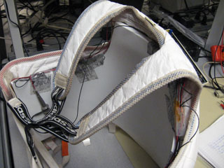
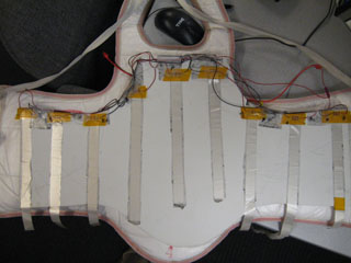
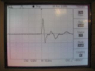
Initially we attempted to implant accelerometers into our hogu. After a couple of days of experimentation the accelerometer idea was dropped. The main reason for not pursuing the use of accelerometers was that they are unreliable. The unreliability stems from the accelerometers inability to differentiate motion from impact. If the hogu is stationary and a force is applied to it, the accelerometers will output a voltage as desired. However if the hogu is in motion the accelerometers will also output a voltage, which is undesirable. We searched for an alternative and came across piezoelectric sensors. These sensors output a voltage upon impact but output only a very small voltage when in motion. We were able to sample nine sensors and implanted them into the hogu. The sensors do not need to be connected to a power supply for operation. Each sensor has a negative lead and a positive lead. All nine negative leads are soldered together and all nine positive leads are soldered together. The negative leads are not a hard ground so they are connected to the MCU ground on the prototype board. The output voltage is taken between the positive leads and the MCU ground. The output voltage waveform is related to the force of impact, which is proportional to the acceleration of impact. A solid strike can result in peak output voltages around 15V. The output voltage is cut by a voltage divider to produce lower voltages which are more meaningful. This is explained in the section below.
Voltage Divider
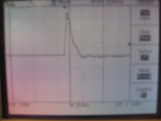
The voltage from the hogu is put through a voltage divider consisting of 51k and 20k resistors and the output is taken across the 20k resistor. The output voltage is approximately 0.28 times the voltage from the hogu. The output voltage of the divider is sent to the lowpass filter. One notable fact is that the LM368 op-amp that is used to construct the lowpass filter is not rail-to-rail. When the rails of the op-amp are 5V and ground, any input waveform whose peak-to-peak is more than approximately 3.8V will have an output waveform whose maximum peak-to-peak voltage is capped at 3.8V. This is the reason for the usage of the voltage divider; that is, the divider allows for better quantitative analysis. For example, consider a very simple hit detection scheme where if the hogu is punched hard enough so that its resulting waveform has a peak voltage greater than 10V, then a hit is detected. Assume two different punches create two waveforms with 5V and 20V maximum peak voltages respectively. The first punch should not be considered a hit while the second one should. However without the voltage divider the lowpass filter will cap both waveforms so that the maximum peak voltage is 3.8V. When the MCU analyzes the two waveforms it will see the two punches as the same when in reality they were not. With the voltage divider the 5V waveform will be cut to 1.4V and the lowpass filter will not cap its output. The 20V waveform will be cut to 5.6V and the lowpass filter will cap its output. The MCU will now see two different punches.
Lowpass Filter
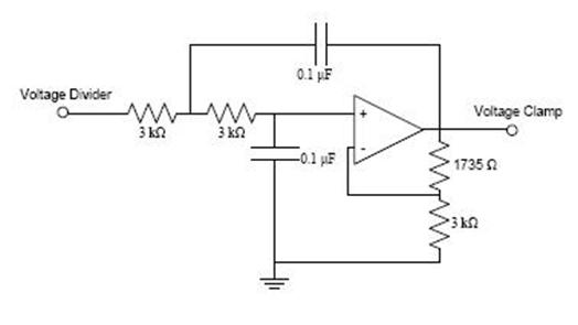
Voltage Clamp
Prototype Board MCU
The prototype board with an MCU computes whether the hogu was struck hard enough to register as a hit. The methodology behind hit detection is described in section 3.1.1. If the MCU determines that a hit is detected then the wireless transmitter will transmit a specific byte of data to the wireless receiver at the lab station. The MCU connected to the receiver will write to the analog TV if the specific byte of data is received.
Wireless Transmitter
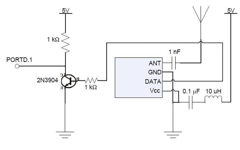
The input to the wireless transmitter circuit is PORTD.1, the TX port on the MCU. The MCU determines if the hogu has been hit sufficiently hard and sends a specific byte of data to signal a hit. The RCT-433 transmitter is the main component of the wireless transmitter circuit. The theory behind its operation is On-Off-Keying (OOK) Modulation, a binary form of amplitude modulation. The transmitter is off when a logical 0 is being sent and is on when a logical 1 is being sent. When the transmitter is idle it sends logical 1's, thus causing constant transmission. It is recommended to invert the DATA input so that the transmitter sends logical 0's in its idle state. The inverter is achieved through the 2N3904 npn transistor. The resulting benefit is that no power is consumed when sending logical 0's because the transmitter is off.
Meghan Desai's wireless protocol[4] was used to transmit and receive data. Parts of the test transmit code tx.c that were necessary for our project's purposes were integrated with our code for the MCU on the prototype board. Details of the integration can be found in section 3.1.1.
3.2.2. Receiver Side
Wireless Receiver
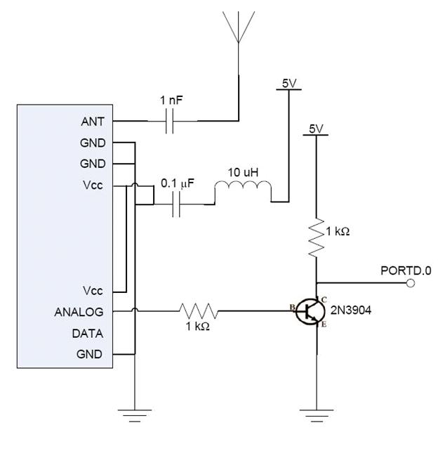
Lab Station MCU
The MCU at the lab station is mounted to an STK500 board and is connected to the wireless receiver circuit through PORTD. The MCU checks if the specific byte of data that corresponds to a detected hit has been received wirelessly. Once the byte has been received the MCU writes the current score to the analog TV. The MCU also has the ability to display penalties. A penalty can be given by pressing a switchbutton on the STK500. The methodology behind wirelessly receiving a hit signal, keeping track of score and penalty, and writing to the TV is described in section 3.1.2.
TV
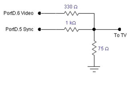
The figure showing the necessary connections between the MCU and the TV is shown on the ECE476 website and is reproduced below for convenience.
The project overall was a success but like everything in life, nothing is perfect. The 1st imperfection I'd like to address has to do with the reliability of the design. Although we do receiver our own transmitted packets most of the time, there are times when we fail to receive data. This prompts the need for a packet loss-less system which is mentioned by Meghan in her report but could not be duplicated here due to equipment and time restraints. While our current protocol is ok for use as a demonstration in lab, olympic level competitors would not be very happy with this project let me tell you that.
With that in mind, our 2nd problem came in the form of improper data encryption. Working in a contained lab is different from outside and sending our packets as ID-tagged alone is not enough to prevent them from being tampered with. A method we looked into was to do a checksum to do a simple redundancy check to make sure our packets were indeed ours in case someone else were using the same scheme as us. Other encoding/decoding methods were looked into but unrealistic given our time frame.
A 3rd problem albeit minor was some flickering to the screen while changing scores. This is probably due to our hack of turning the timer off and on while writing the score.
While safety in this project was probably of the utmost concern out of all of them, we kept ourselves relatively safe. No nonsense or horseplay was tolerated with our design and everything was kept professional.
For recreational and sports analysis purposes, we believe that this product is a great tool that can be used for training and commercial purposes; however, it is far from perfected and cannot be qualified for olympic level competitions. Major issues such as a proper data encryption scheme and packet loss-less system prevent our system from being as high quality as that of a company such as Adidas, but we believe that we created a reasonable prototype simulating electronic impact detection.
Ultimately, I would like to call our project a success but in retrospect there are a multitude of possibilities that could have been done given more time and resources.
The hit detection scheme implemented on the prototype board MCU is our own code. We implemented Meghan Desai's wireless protocol into our project. We used what we learned in Lab4 to write to the TV.
We signed a non-disclosure agreement to sample the piezoelectric sensors. Therefore patent opportunities are unlikely. Also there are companies that are commercially producing electronic hogus so they're design and implementation is likely to be better and more advanced. This diminishes our patent opportunities.
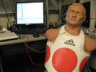
Decisions and actions taken during the project were consistent with the IEEE Code of Ethics. Safety is a key issue. Our project involves the striking of a hogu that is normally worn by a person. We have never let anyone don the hogu during this project. Instead we tied the hogu to a chair and eventually brought in a punching bag mannequin to wear the hogu. We also worked at stations where there was enough room to punch or kick the hogu without injuring anyone nearby. In terms of hardware we kept all boards on the lab station's grounding mat when applying voltages to them. At the soldering station we wore goggles to protect our eyes.
We avoided conflicts of interest by signing a non-disclosure agreement with Jin Song, the provider of the piezoelectric sensors. The NDA requires that Jin Song's company's competitors do not benefit in any way by our having sampled the sensors. Also Jin Song will have the rights to all our experimental results and developments that arise during our involvement with this project. We have never had conflicts of interest involving money because we have not faced bribery in any form.
We have not been dishonest nor unrealistic in our claims of delivering our final project. Our project proposal stated that we will develop an electronic hogu with a hit detection scheme and wireless capability, and we have achieved our projected goal. And through this project we have improved our understanding of multiple aspects of technology. We have learned how piezoelectric sensors work and how to use them in real-world applications. We have learned how to implement wireless communication with the help of Meghan Desai's wireless protocol. We have learned how to view our project at the systems level. At the same time we have improved our existing technical abilities ranging from knowing how to build filters to soldering hardware.
We have sought input from other peers about our project and have accepted concerns and comments as they came. At the same time we gave our own inputs and thoughts to our peers.
We have never discriminated against anyone based on any factors including race, religion, gender, disability, age, or national origin.
In order to sample the piezoelectric sensors it was required to sign a non-disclosure agreement with the provider of the sensors. The NDA outlined that the provider's competitors will not benefit in any way from our sampling and that the provider will have access to all our experimental results and developments.
There were FCC regulations[5] to consider because of our use of wireless transmitter (radiator).
The FCC sets regulations under which intentional radiators may be operated without license. The FCC defines an intentional radiator as a device that intentionally generates and emits radio frequency energy by radiation or induction. Nearly all of the FCC mandates do not apply to us, but while a few of them are applicable we ultimately abide to all the rules. Our wireless device is 'home-built' but equipment authorization is not required because no more than five devices are built. This also implies that our wireless device is not a Class A device, which is defined to be a digital device that is marketed for use in a commercial, industrial or business environment. The operator of an intentional radiator may not use an antenna that is furnished by any party other than the operator. This is fine since we made our own antenna using a wire. The frequency 433.92MHz is not restricted nor does it cause any harmful interference.
If the FCC ever contacts us we will obey all directives and provide all information regarding our wireless device.
| Part | Quantity | Unit Price |
| Whiteboard | 1 | $6 |
| STK500 | 1 | $15 (Lab Supplied) |
| Piezoelectric Sensor | 9 | $0 (sampled) |
| Hogu | 1 | $0 (previously owned) |
| Prototype PCB Board | 1 | $5 (Lab Supplied) |
| Atmega32 MCU | 1 | $8 (Lab Supplied) |
| Solder Board | 1 | $1 (Lab Supplied) |
| RCR-433 Receiver | 1 | $4 (Lab Supplied) |
| RCT-433 Transmitter | 1 | $4 (Lab Supplied) |
| Power Supply | 1 | $5 (Lab Supplied) |
| LM368 Op-Amp | 1 | $0 (Lab Supplied) |
| 2N3904 NPN Transistor | 2 | $0 (Lab Supplied) |
| Various Capacitors | 6 | $0 (Lab Supplied) |
| 10uH Inductor | 2 | $0 (Lab Supplied) |
| Various Resistors | 13 | $0 (Lab Supplied) |
| IN914 Diode | 2 | $0 (Lab Supplied) |
| LED | 1 | $0 (Lab Supplied) |
| Analog TV | 1 | $5 (Lab Supplied) |
| Wire | Many | $0 (Lab Supplied) |
| Total | ~$53 + small parts |
| Kevin Kim | Howard Kim | Together |
|---|---|---|
| Prototype Board | Wireless | Systems Level Design |
| Software Test/Debug | Hardware and Circuits | Lab Report |
| PCB MCU Code | Hardware Test/Debug | Website |
| Receiver MCU Code | TV Display Code |
RCR-433 Datasheet: http://www.radiotronix.com/datasheets/rcr433rp.pdf
RCT-433 Datasheet: http://www.radiotronix.com/datasheets/RCT-433-AS.pdf
[4]Wireless Protocol: http://instruct1.cit.cornell.edu/courses/eceprojectsland/STUDENTPROJ/2005to2006/mpd25/report.html
[3]]Wireless Circuitry: http://instruct1.cit.cornell.edu/courses/ee476/FinalProjects/s2006/acd32ddk26/Antonio%20and%20Donn%20Final%20Project.htm
[1]: True Score Pricing List
[2]: CNN Video Interview w/ Ed Chi and Jin Song