Networked Biometric Authentication
Peter Greczner
Matthew Rosoff
| INTRODUCTION | DESIGN | HARDWARE | SOFTWARE | RESULTS | CONCLUSIONS | APPENDIX |
|
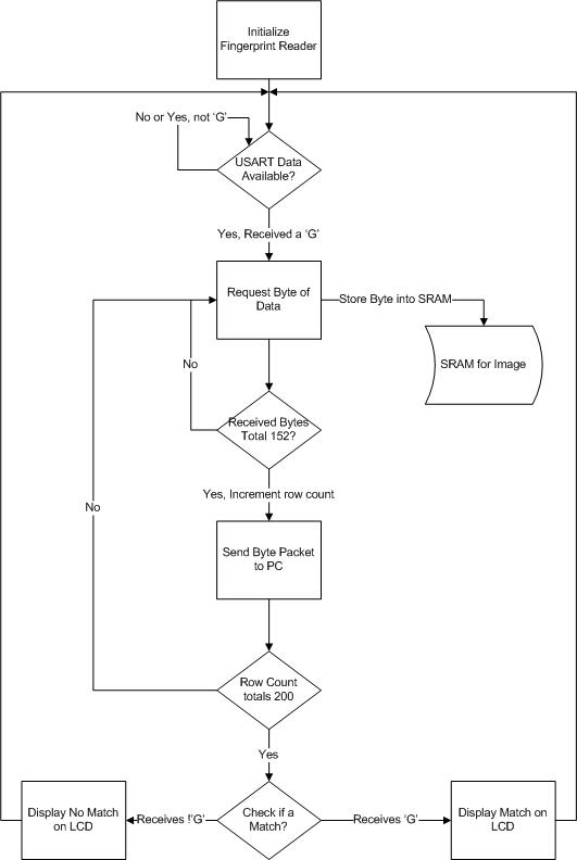
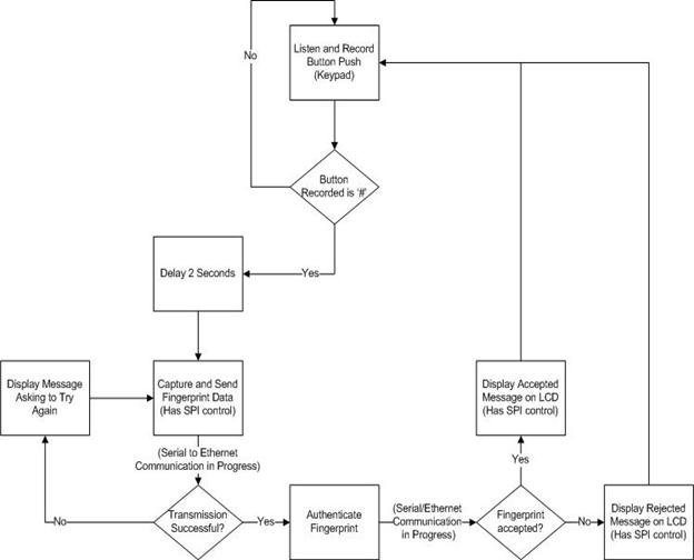
This project produces a system that captures a user’s fingerprint and then authenticates it against a database via Ethernet communication; authentication results are displayed via two color LED's. Introduction:Due to the increasing need for securing data and places, the biometric authentication industry is seeing large market growth. We decided to build a scalable, small, and efficient device that can be used to secure doorways throughout a complex. We use a FingerPrint Cards capacitance based fingerprint scanner as our capturing device. This data is captured through use of an ATMega32 microcontroller and stored on external SRAM while being sent through the microcontrollers USART serial port into a serial to Ethernet converter to a server computer. This computer then performs the filtering and authentication and sends the result back over Ethernet to the microcontroller. High Level Design:Rationale:Security is becoming increasingly important in many facets of society, ranging from military, corporate world, and personal lives. One area of technology that is seeing growth is that of biometric authentication where a user is granted access to a piece of data, room, etc. via some form of biometric authentication. This market saw revenues of approximately US $3.01B in 2007 and is projected to reach US $7.41B by 2012; fingerprint authentication is expected to reach US $400M by 2010. This need for securing data and places effectively, coupled with the project market growth of the biometric industry, led us into a project where we created a system that uses fingerprint biometric authentication for a user to enter through a doorway.Fingerprint Capturing:To capture the fingerprint image we set the microcontroller to wait for an available character in USART. When a character becomes available, it reads it, and if it is equal to ‘G’ then it starts the image capturing. We then read in the stream from the fingerprint reader and simultaneously store the data point in SRAM and add it to the Ethernet packet for later transmission. The result of the matching is then outputted on the LED's. Once all 30400 bytes have been sent, the microcontroller returns to waiting for another read. The logical structure is illustrated below:
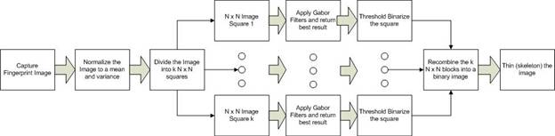
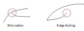
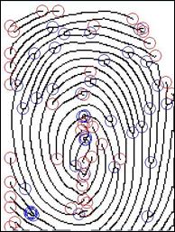
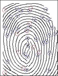
Fingerprint Verification and Background Math:There are basically three steps to matching one fingerprint against a reference fingerprint in a database. The first step is to perform the filtering on the input fingerprint in which the goal is to enhance all features and end up with a “skeleton” image of the original fingerprint. Step two is to take this skeleton image and find as many legitimate minutiae (ridges and bifurcations) as possible. The last step is to compare the legitimate minutiae that were just found against the reference minutiae in the database and output the result (true or false) of the comparison. Step One - Feature Enhancement:
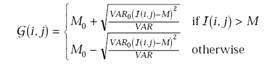
Normalization:
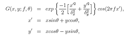
Gabor Filtering:
Threshold Binarization:
Thinning the Image: Step Two – Minutiae Extraction:
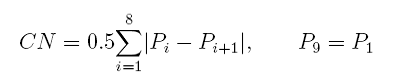
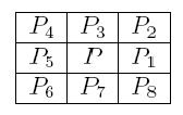
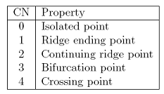
After minutiae are identified as being possibly legitimate we attempt to delete all of the spurious minutiae. The first class of spurious minutiae that we eliminate are those on the border and those near regions of low variance in the initial fingerprint image. These are eliminated because often the minutiae finding algorithm will mark them as ridge endings since they stop at the border of the windowed image. The second class of spurious minutiae are those that are very close to each other; either ridges very close to ridges, or bifurcations very close to bifurcations. This is done because if minutiae are very close, then what most likely has happened is that the original fingerprint is of poor quality and the enhancement techniques could not fully reconstruct. Determining of “too close” is done via a simple distance formula and a threshold of about the ridge period. Step Three – Minutiae Comparison:
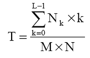
The goal of the algorithm is to find out the Transformation T that maps the Query Set, Q, to the Template set, T, with the smallest amount of error. The transformation T can be generalized by a rotation and a x,y translation.
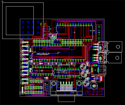
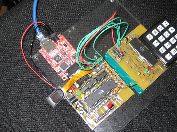
Hardware and Software Tradeoffs:We had two options for having a user log their name into a system for verification – we could perform a Hyperterm type of method of typing the name into a console and sending that to the microcontroller, or we could use a peripheral, the keypad, and read in and debounce the data received on one of the ports. Do to the original design of our project in which we wanted to create an authentication system that was small and could easily fit on a wall next to a door, it would not be reasonable to expect a full functioning computer and keypad to be sitting right next to the door, and thus opted to go with a more hardware approach with the keypad.There was also the tradeoff of using a dedicated chip for processing and filtering the fingerprint images versus using a PC to do the processing. The disadvantages to the dedicated chip were that it would be slower, possible add in an extra ATMega32, and would add extra cost to the unit. The benefit of a dedicated chip would be that all processing could be performed before sending of minutiae data, and thus the client side PC could possibly handle more simultaneous request. The benefit to using a PC was significant less cost since we would already be using a PC for matching to the database, and also in a large scale application the PC’s performing the calculations would be very quick. In the end we felt that the proper implementation would be to go the software route and perform the filtering and matching on a PC which received data from the microcontroller. Standards: Hardware Design:The hardware design for this project consisted of us interfacing the peripherals (sensors, memory, keypad, and LCD) with the ATMega32. Due to the complexity of these interactions we also needed to design a custom PCB board to handle this.PCB Board Design:Given the amount of custom hardware and interconnects, neither a standard 476 proto- board nor a perf-board would suffice for our project. A custom-made printed circuit board was our only option in order to accommodate the LCD screen and the fingerprint sensor’s FPC connector.The circuit board was created first as a schematic in Eagle Cad, and was then routed in Eagle Cad’s board layout mode as a double-sided PCB. Sunstone Circuits printed the boards and granted us a generous sponsorship, allowing us four free PCB’s. Unfortunately, we could not afford a solder mask, which would have made soldering the LCD connector easier. Instead, we experienced a 50% rejection ratio when soldering the LCD connector (0.5 mm pitch). Additionally, since the board was our first revision of the circuit, there were a few design errors that had to be corrected by cutting 3 traces and soldering jumper wires on the underside of the board. Our PCB’s are mounted on 0.25” Lexan (Polycarbonate) in order to avoid short circuits on the underside of the board and to enhance the aesthetic appeal of our project.
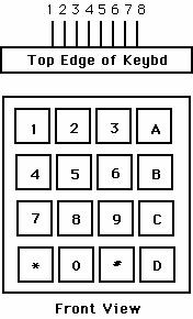
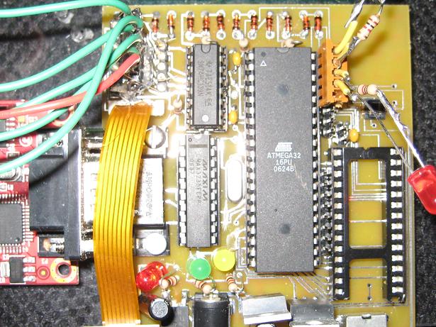
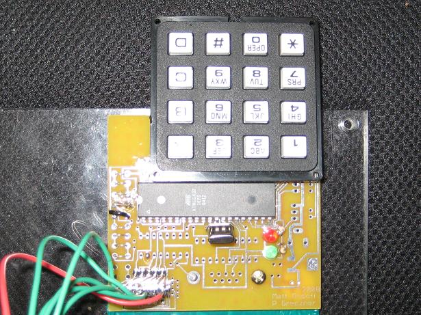
Serial Peripheral Interface (SPI):The LCD display, keypad, and the fingerprint sensor were operated via serial peripheral interface (SPI). The chip select on both of these were active low, so we therefore decided to use a 2 to 4 active low decoder. This meant that we would have two bits specifying the particular SPI interface. This bits corresponding to PORTB.4 and PORTA.7. Fingerprint Sensor:The fingerprint sensor that we used was the FPC1011C by Fingerprint Cards AB. This is a capacitance based fingerprint sensor with an internal A/D converter and provides an SPI interface. The operating voltage for this sensor is 3.3 volts. Since the voltage that we are providing to our board is 5 V this required us to use a 3.3 V voltage regulator. The sensor is connected to the microcontroller via the SPI ports.The physical interconnect on the fingerprint sensor is a 10-wire FPC ribbon cable. This cable is impossible to solder directly, so a mating connector, manufactured by Molex, was used to mount the sensor. SRAM: Our project utilized parallel SRAM to store fingerprint images quickly. The SRAM is ~32KB, and can hold one image. Because of the size of the SRAM, 15 address lines were needed to address each byte in memory (215 = 32KB). Additionally, 8 data lines, and 2 control lines (OE’ and WE’), were needed. Since there were so many pins, and we were trying to keep hardware to a minimum, we connected the least significant address bits to PORTC and the most significant address bits to PORTA.0-6. CS’ connects to PORTD.2 and OE’ connects to PORTD.3. SRAM operates at 5V logic levels, compatible with the master MCU. The SRAM consumes most available pins on the ATMEGA32, so all other peripherals need to operate on the SPI port. Keypad:Port C was used to handle our alpha-numeric keypad. The keypad had 9 pins, but only pins 1 – 8 were needed. The pinout was C.0 went to pin 1, and C.1 to pin 2 ... C.7 to pin 8. The Keypad used the Auxillary ATMega32 SPI interface to send its data to the main ATMega32. This SPI was configured as a slave.
Figure 1 – Keypad pins
LCD:The LCD screen was also interfaced with via SPI protocol. We used an EPSON S1D15G10 color LCD display. When using this display the SPI was configured to act as a master during communication, with SS active low, MOSI, and SCK acting as outputs. We did not require MISO to be an input because no data was needed to be read from the LCD display.Voltage Regulators
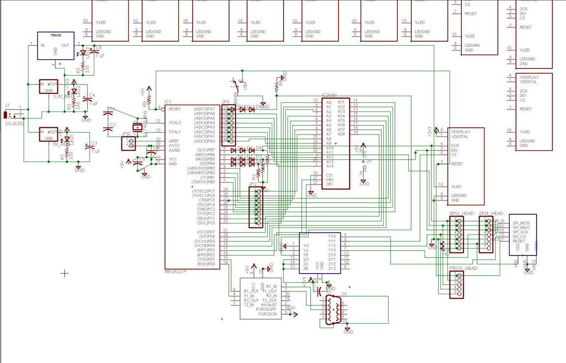
Our project needed three operating potentials: 3.3V, 5.0V, and 6.0V. The SPI bus and the CS’ decoder uses 3.3V, the MCU, SRAM, and MAX3235 use 5.0V, and the LCD uses 6.0V for its backlight. Therefore, three voltage regulators are needed to supply the operating voltages for the components. Linear regulators, although inefficient, are used because they are inexpensive and produce very little noise on the supply lines. Clearly, this creates a problem where data is being sent and received at different voltages. A step down circuit, outlined below (three 0.6V diodes in series) performs voltage down-conversions. Voltage up-conversions are not necessary because the 5.0V devices accept 3.3V inputs. Serial and Ethernet Communication:We used the WIZ110SR serial to Ethernet converter to handle our Ethernet an serial communications. There was no hardware design on our part for this conversion process, but we did need set the parameters for the ATMega32’s USART communication, as well as connect their pins appropriately to the serial ports. The port connections were done on the PCB board, and the parameters were set via software.The full circuit schematic of our project is illustrated above. You will notice two different pictures. One picture is that of the port and peripheral connections in a schematic layout; the other is that of the PCB board that was designed and built for implementation of the hardware. Clocks:A 14.7456 MHz crystal provides the master MCU with a clock. This XTAL is unique because it provides the USART with a clock to send data at high rates (230.4 K) with little error. The clock on the auxillary board was 8 MHz.Timers and Interrupts:We also had to use timer2 on the ATMega32 as a timer for controlling the debouncing of our Keypad. We set timer2 to a prescaler of 64 with OCR0 = 250. We also implemented the TIM2_COMP interrupt. This interrupt would be executed a little under every millisecond (250 / (8 MHz / 32) = 0.001 seconds = 1.00 ms. By setting our keypad task counter to 30 and executing it’s debouncing task every time the counter reaches 30 this allowed us to debounce once every 30.0 ms, or about 33 times per second, which is faster than a human can punch in their keys.Software Design:Our software was responsible for performing the following essential tasks – sending and receiving data through serial to Ethernet communication, saving data to SRAM, sending information to the LCD, receiving data from the fingerprint scanner, and reading keypad input.
Handling Keypad Input: In order for us to take in keypad input it required that we debounce the keypad. We used the following schema for reading input and debouncing the keypad:
Writing to the LCD:We were never successfully able to write to the LCD. The hardware was implemented, but the SPI interface for the LCD proved difficult. This could have been a product of faulty settings issued to the LCD, or the LCD could have been broken. We do not believe that it was an SPI issue because SPI successfully worked for the keypad and the fingerprint scanner.Writing to SRAM:Synchronous Random Accessed Memory, or SRAM, is a fast and simple way to expand a microcontroller's memory space. The SRAM used in the project is pulled from an old STK board. It has 15 address lines, 8 data lines, OE' and WE' lines. To store data, data is placed on the data bus, the address is loaded, and the WE' line is strobed low. To read data, the address is loaded, the OE' line is strobed low, and data is sent back the MCU on the data bus. Because SRAM requires 25 data lines, setting up the address and data can be a bit daunting at times. The address is stored in two sequential registers as an int using the pragma –regalloc. There are two pointers to the MSB and the LSB of the int so that loading these bytes onto the 15 address lines can be done in a single operation. The data is trickier because the low order nibble is placed on B0-B3 and the high order nibble is placed on D4-D7. To perform this operation, PORTD=(PORTD&0x0F)|(data&0xF0). This preserves the low order nibble on PORTD while writing the high order nibble. Unfortunately, placing the data takes 8 cycles, placing the address takes 2 cycles, and strobing the appropriate control lines takes 2 cycles, making a read/write 12 cycles, or 750 ns. This is significantly slower than the approximate 100 ns read/write time for SRAM, so the code is well within the timing parameters.Serial to Ethernet Network Communication:
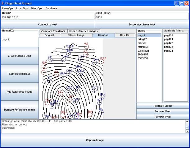
For our serial to Ethernet network communication we used the serial to Ethernet converter chip WIZ110SR by Wiznet. We configured this device to act as a server which held packets of data for us. Since this acted as a server, on our PC side program we create a socket to connect to it’s serving port. To send data to the WIZ110SR we use the ATMega32’s serial communication. Every time we want to send a byte we set UDR = (byte)someData for the USART communication. Once we have sent the number of bytes to the WIZ110SR that is equal to it’s packet size (153 in our case) the packet is sent to our PC client program. To receive data on the ATMega32 we implement a wait loop to see when the UDR’s receive buffer is full. Once it is full we read the data from UDR (data = UDR). The receiving of data does not depend on packet size. Therefore we used a system of ‘G’ood and ‘F’ail for commands that would be sent from the client PC to the microcontroller. When the microcontroller is attempting to read in a byte and it reads in a ‘G’ it processes a successful attempt. When it reads in a byte other than a ‘G’ it processes a failed attempt at communication. A diagram of this communication was illustrated above. PC Client InterfaceThe client interface on the PC side was written in Java. More information regarding this side of the project can be found in the appendix section. Results and Analysis:The following table is a list of parameters and corresponding results that are important to our authentication system.
In a system like this the timing properties of are high importance, because when someone wants access through a portal they would like it in a reasonable time. A user will usually sacrifice the time it takes to type in the code for the authentication time. From the time a user types in our code to the time a user is verified takes about 15 seconds. The image capture time, includes the sending of data through Ethernet and being captured by the authenticating computer; this time is reasonable. The image filter time is the time is the time from when the image is received to the time it has been filtered. This will be the longest part of any authentication process as it requires heavy filtering computation. The time it takes for us to filter on an Intel Core2Duo E6600 overclocked to 3.4GHz 2GB RAM (a fast computer) is about 5 seconds. The last criteria is the minutia comparison time, and we found this to be anywhere from about a second to five seconds depending on the number of images in the database for a person.
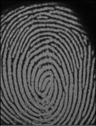
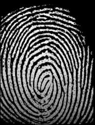
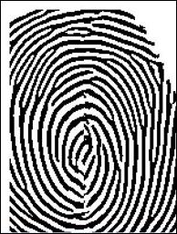
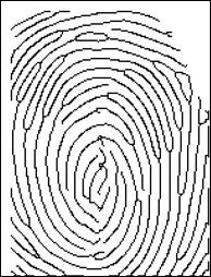
For an authentication system the two parameters FAR and FRR are probably the most important. These represent how secure the authentication is. One would rather have FRR higher than FAR, since it is better to reject someone who belongs, rather than accept someone who shouldn’t be accessing the portal. Both of these are proportional to filtering time. The more exact you filter and match, the longer the filtering takes, but the lower the FAR and FRR. There needs to be some tradeoff. These two sets of data also depend on how many fingerprints you match to for a user. Having a large set of reference prints will help reduce FRR because we have many images for a user to accept to. However, with more images induces higher chances for error, and thus could raise the FAR. Our results of both FRR and FAR being less than 10% is an acceptable result within the scope of our project. This means that only 3 in 40 users will be granted access who shouldn't be granted access, and at the same time only 3 in 40 users will encounter frustration with failing a test when they shouldn't, and then have to try again. Depending on the level of security of who is using this device the fact that our system lets 3 in 40 improper users in may or may not be acceptable. The security of this device could further be enhanced by certain operational proceduers. One such procedure would be to have all users keep their 7 digit identification private. Our testing assumed that any other user could know any other users ID and try and fraud the system. But, if ID's were private, the error rates would go down due to the fact that it would be much more difficult to fraud the device. The acceptance criteria number is the threshold on which we accept or reject a fingerprint. It is solely a result of the matching algorithms computations. For our test runs the value of 0.0800 was used. This value can be either hard coded into the software or dynamically set at runtime. The filtering results of an input image are shown below. You can notice below that we were able to reconstruct a somewhat noisy image into a very accurate binary thinned reproduction. The only area of concern for this filtering is in the very center swirl where the filtering has trouble accepting the small radius and rapidly changing angles of orientation. This is a product of the gabor filter.
Usability and Safety:This project is able to be used by any company or industry that wants to implement a low-level security biometric authentication system for their networked building. The final size of the board is approximately 9” x 9”, is user friendly, and only cost us about $75. There are still a few quirks to work out before such a product would be put into final production, but the ground work is all there for large scale integration. Conclusions:We believe that this project turned out to be a success of its original mission. We set out to develop a networked biometric authentication system and this is exactly what we achieved. A user is able to be registered and stored into a database, they can then enter their id and scan their fingerprint which is then authenticated and the result is sent back locally to the microcontroller. Intelluctual Property Considerations The only imaginable intellectual property violation considered is that of the fingerprint matching algorithm. The brute-force fingerprint matching algorithm was mentioned in various texts as a simple algorithm that had moderate success in matching fingerprints. However, in our opinion, this algorithm is more public knowledge than intellectual property because the algorithm appears in many commercial and hobbyist projects. No single company has taken the rights or royalties on the algorithm. Some variations and improvements on the algorithm have been posted in scientific journals, but we did not take a novel approach toward matching. The PCB design could be considered intellectual property and could be protected under law. Ethics, Legality, and Standards Compliance Ethically, we could run into a conundrum where some guests don't want their fingerprint stored in a database, but would like access to a particular secure area. Some users may not know that when they put their finger on our scanner, their fingerprint may be stored in a database, and could be subpoenaed in a court of law. Perhaps a sign is needed above the sensor, or perhaps it is assumed that upon gaining access privileges, the user enters a contractual agreement to provide fingerprints. Fortunately, our system is not commissioned for general public use, so any private applications or implementations should avert this ethical / legal debate. Our project complies with all SPI / RS 232 / and Ethernet standards, as posted by the IEEE because all components are certified for use in these areas, and all circuitry for these communication protocols is implemented by reputable designers, like Atmel, MAXIM, etc, for commercial use. Appendix:
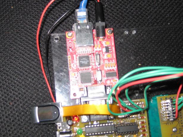
Figure - Fingerprint sensor and serial to Ethernet converter Cost Details:
Specific Tasks: References: ATMega 32 Datasheet Epson S1D15G10 LCD Datasheet Fujitsu MB84256A SRAM Datasheet Fingerprint Cards FPC1011C Fingerprint Scanner Datasheet . Acknowledgements:We would like to sincerely thank Sunstone Circuits for their generous sponsorship of PCB boards so that we caould complete this project. We'd also like to thank the many other electronic companies from whom we sampled components from.
~Peter Greczner, pag42@cornell.edu
|