NES EMULATION
By:
Tom Gowing (teg25) and Brian Pescatore (bhp7)
OVERALL
DESIGN GOAL
The overall
goal of our project was to recreate the Nintendo Entertainment System (NES)
using Atmel Microcontrollers. We decided early on the adding audio to the
mix was likely going to be too much work in the time that we had to complete
the project. Therefore, we decided to leave all audio aspects out of the
mix. Therefore, our focus became emulation of the modified MOS6502
processor that the NES used as the CPU and the generation of the video.
It was determined, however, that the video generation that was done by the
Picture Processing Unit (PPU) was too complex to be entirely done in software,
or even used limited hardware (See below for a discussion on the methods of the
NES PPU). Therefore, what remains of our project is the 6502 emulation,
cartridge reading, controller input, and memory mapped I/O
synchronization. The lack of video, however, was not something that we
wanted to settle with, so we decided to show off some of the video tactics that
were utilized by the Nintendo. Our video
outputting scheme must fully comply with NTSC standards. We achieved this compliance by using a
specialized chip (AD724) to convert Red/Green/Blue into NTSC.
Development
of the NES 6502 Emulation
The 6502
was an evolutionary microprocessor that was widely used for one reason: it was
absolutely dirt cheap compared to the rest of the functional microcontrollers
on the market. The modified version of the 6502 that the NES uses was
also quite cheap to produce, which is why ten years after production of the
product Nintendo was still asking for the far outdated 6502. The main
differences between the two chips involve the I/O line designations as well as
the addition of the pseudo-Audio Processing Unit (pAPU). The added I/O
lines include five that are devoted to obtaining data from the controllers and
two that are used as audio output channels.
The
interesting part of the NES 6502's operation is that there were absolutely no
additions to the instruction set available to the programmers of the NES
games. The raises the obvious question: how does one read from the
controllers or generate the newly supported audio? The answer to that
lies in the memory mapped IO which is the basis for nearly all communication on
the NES.
The
memory-mapped IO is a series of memory addresses which, when written to or read
from, produce side effects in other aspects of the hardware. The basic
set of IO ports are listed below, and it should be noted that additional IO
ports can be added via use of Memory Mapping Chips (MMCs) which would be
hardwired into the game cartridge to expand the capabilities of the NES. (This
project does not deal with interfacing to any particular MMC but rather passes
most all addressing out to the cartridge where any present MMCs are given the
opportunity to react to the programmed signals. Therefore, we will not
discuss the MMCs any further, but point interested parties to the references at
the end of the document.)
|
Memory
Address |
Purpose |
|
$2000
|
PPU
Control Register 1 |
|
$2001
|
PPU
Control Register 2 |
|
$2002 |
PPU
Status Register |
|
$2003 |
Sprite-RAM Address Register |
|
$2004 |
Sprite-RAM
I/O Register |
|
$2005 |
Video
RAM Address Register 1 |
|
$2006 |
Video
RAM Address Register 2 |
|
$2007 |
Video
RAM I/O Register |
|
$4000-$4013,
$4015 |
pAPU
(Audio) Control Registers |
|
$4014 |
Sprite
Direct Memory Access (DMA) Register |
|
$4016 |
Controller
1 Access Register |
|
$4017 |
Controller
2 Access Register |
The
registers listed above are merely "views" at data registers contained
within other hardware (PPU registers being hardwired address correlations to
the video processor and audio registers being internal latches in the NES 6502
that output to specific audio generating hardware. These registers will
be referenced directly in points hereafter, at which time the uses of all
imperative registers will be explained.
Of course, behind the intertwined hardware and IO connections, at the heart of
the NES 6502, is the slightly modified version of the original 6502, and
therefore emulation of this hardware is the forefront of the project.
The general
method of emulating a processor is to completely replicate the functions of each
individual operation that the processor can handle. The 6502, while the 8
bit opcode could support up to 256 instructions, only 151 of the 256 available
opcodes has defined behavior (In fact, using other instructions opcodes not
necessarily produce no operation, but may in fact send your program into
complete disarray.) Furthermore, these 151 opcodes only actually support
56 distinct operations, with specific opcodes merely varying the addressing
mode utilized by the operation (see addressing modes below).
Along with successful emulation of all instructions, we must establish
successful emulation of all registers. The registers present on a 6502
are as follows:
- Program Counter (PC): 16-bit pointer to the next
instruction to be executed.
- Stack Pointer (SP): 8-bit pointer into the stack.
- Accumulator (A): The key arithmetic register for nearly
all operations.
- Index Register X (X): A register typically used for
indexing and counting. Additionally can be used to stack pointer
transfers.
- Index Register Y (Y): A register typically used for
indexing and counting.
- Status Register (S): Contains flag pertaining to the
preceding operation.
Status Register
Layout (Bit7 - Bit0)
|
N |
Negative |
|
V
|
Overflow |
|
-
|
ignored |
|
B
|
Break |
|
D
|
Decimal (use BCD for arithmetic) |
|
I
|
Interrupt (IRQ disable) |
|
Z
|
Zero |
|
C
|
Carry |
(Note that the modified 6502 used in the NES did not support BCD mode, but did not
bother to remove the opcodes that set and clear the flag, therefore providing
another conditional flag which can be set and branched upon at will.)
Of the above registers, the
only one that requires more than a variable in the program is the stack pointer.
Along with the stack pointer is the need to implement a stack directly into the
data memory of the Atmega644. For the NES, this stack was located in the
memory, addressed from $100 to $1FF. In addition, the 6502 did not
contain and safeguards on the length of the stack, and if one was to push over
256 elements onto the stack, they would wrap around and start trashing the
lower bytes of data. In emulation, in is not pertinent to worry about
this overflow either because this fact is known by the programmers and was
either avoided, or in extremely rare cases, used to the programmers advantage.
The available opcodes operate on the aforementioned registers. They are
broken down into a few sets of operations:
- Load / Store Operations
- Register Transfers
- Stack Operations
- Logical Operations
- Arithmetic Operations
- Increments & Decrements
- Shifts
- Jumps & Calls
- Branches
- Status Flag Changes
- System Functions
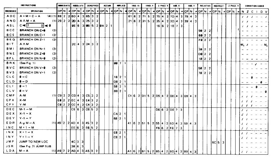
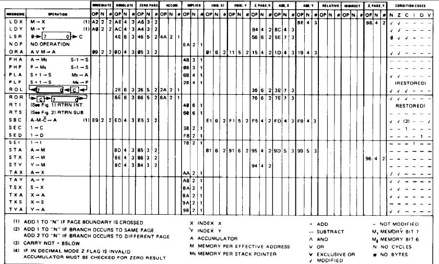
For a full list of operations, see the table at the end of the document.
Emulation of the 6502 requires working with the 13 different addressing
modes. These addressing modes work as follows:
There are many instructions in the
6502 processor that have "implicit" targets, such as "Clear
Carry Flag" (CLC) and "Set Interrupt Disable" (SEI), meaning
that the operation is only defined to work at those specific points. This
allows implicit instructions to take up only one byte of program memory.
Accumulator
Accumulator
addressing means that the instructions work directly upon the accumulator
register. In a sense, these are also implicit by nature, with the only
exception being that the implicit address is always the same.
Immediate
addressing allows the use of an 8-bit immediate offset by the programmer
directly in the code itself. Instructions using immediate addressing take
two bytes of memory.
Zero
Page addressing mode is the most efficient way of accessing actual
memory. Addressing in this manner simply means that the address is
located in memory $00XX, and therefore will only take two bytes of memory
because only one 8-bit address is required for addressing.
Zero
Page, X addressing will essentially restrict your memory field to only the
first page of memory (256 bytes). It first takes the zero page address
and then it adds the X register to it to produce a 8 bit address. Note
that the address cannot exceed 8 bits, and therefore will always wrap around
from $FF to $00 rather than $100 (which of course is no longer on page zero of
memory). Like Zero Page, this is a two byte instruction.
Zero
Page, Y is essentially the same as Zero Page, X except that the two are not
interchangeable. The only instructions that use Zero Page, Y are the LDX
and STX instructions, load and store X register to/from memory. The only
reason that Zero Page, Y is used rather Zero Page, X is because the
instructions cannot modify the contents of X. Also a two byte instruction.
Relative
addressing is used for branching. It specifies the value which should be
added to the PC upon a true evaluation of the branch condition. This is a
two byte instruction.
Absolute
addressing is when a full 16 bit address is provided ( LSB first) in the two
bytes following the opcode. The specified address is a direct lookup into
the memory.
Similar
to Absolute addressing, Absolute X addressing provides a 16 bit address, but
additionally adds the value of the X register to it before accessing the
memory.
Identical
to Absolute X, replacing the X register with the Y register. (Three byte
instruction)
Indirect
addressing is only used by jump commands. Essentially, the two bytes
after the opcode specify an address in memory which contains the LSB of another
16 bit addressing. It is this address that is the desired destination of
the jump instruction.
Indexed
Indirect addressing adds the X register to the supplied 16 bit address and then
works exactly as Indirect addressing works.
Indirect
Indexed addressing retrieves the 16 bit value stored at the address specified
in the two bytes following the opcode. It then adds the Y register to the
retrieved 16 bit value and uses this value as the jump location.
Emulation
Now
to discuss how the 6502 was specifically emulated. The main goal is to
obviously recreate program control, but the real catch is that we need to maintain
control of the timing elements native to the NES 6502. The NES cpu ran on
a 1.79 MHz clock, which compared to the 16 MHz clock we used for the Atmega644,
gives us approximately 8.5 cycles per native 6502 instruction. Yet there
is still an added bonus to this because the 6502 ran on a base 2 cycle system,
meaning that no instruction took fewer than 2 cycles, and some took as many as
7 cycles to complete. This means that our base timing level is at 17
cycles. Now if the 6502 had only 2 cycle instructions then we would need
to improve the speed of the program in a few places. However, if we
amortize the time taken by a series of instructions in general we are looking
at a very well balanced and time synced emulation.
This is all made possible via
a near exclusive use of #define coding style. Working in this manner,
while it does make the code significantly larger due to the replication of code
in many places, it saves a bunch of instructions on every single
operation. We also need to be careful when working with code in this
manner. When using #defines as a method of increasing the speed of the
code, then you must try to only pass in either a single variable or an
immediate variable into them. If you are careless in their use, you may
end up replicating code along the lines of variable increments or memory
lookups. These kinds of bugs also manage to hide themselves to a level of
total obscurity due to the similar appearance of a function and a #define.
First, we grab the opcode from
the cartridge (The first address of the program is addressed inside of the
cartridge at $8000.) and use that as an offset for a jump command. This
jump is done by executing the jumper function. We use a function for this
because we need to gain access to the internal program counter. We do
this by popping two bytes off the stack which by the nature of function calls
is the program address to which the function will return. We then add the
opcode to this value two times to account for the fact that a jump instruction
occupies two words in memory. The result is pushed back onto the stack
and the function is allowed to return to the desired place within the
jumplist. This jump command will land us somewhere in the jumplist, which
is 256 consecutive jump commands. These jump commands will direct our
program to individual sections that handle each instruction.
At these commands, we need to
indicate three things. First, we need to indicate the size of the
instruction in bytes. Secondly, we need to indicate the addressing mode which
is used. And, finally we execute the actual instruction which the opcode
specified.
Indicating the size of the
instruction is a simple enough operation. The instructions can be either
one, two, or three bytes. The first byte is the opcode, so if the
operation only needs one byte, then we are already done at this point. If
the operation requires any more bytes, then we must retrieve a few more bytes
from the cartridge. These bytes are stored into the instr_byte array (in
the 1 and 2 positions, because the opcode takes instr_byte[0]) and are used in
determining addressing.
In order to accurately setup
the addressing methods and to allow the addressing modes to exist completely
independent of the instructions that are calling them, we need to define a few
variables which will consistently be used, no matter what the instruction
is. This allows us to keep all of our code inside of the main function
and makes the #define method more efficient. While functions would clearly
clarify the code, getting into and out of the functions would waste far too
much time. The variables that we used were rOP(char) and rOPA(int), named
for operand and operand address. Essentially, most addressing modes have
both an address setup routine as well as an extraction routine. The
address setup routine places the address which we intend to work upon into
rOPA. The extraction routine, internally calls the addressing routine and
retrieves that value from the address in rOPA, storing it into rOP.
As stated before, prior choice
of rOP and rOPA make almost all other instructions easy to implement by simply
working with the value in rOP or rOPA. The exceptions to this are rotate
shift operations, which need a post-step to place the value back into memory or
reapply rOP to the accumulator, depending upon the addressing mode. All
other instructions, after making a call to an addressing routine, simply make a
call to the actual instruction routine that was indicated and it will be
carried out. Once completing this, it jumps back to top of the program to
grab a new instruction.
As I mentioned previously,
most instructions involve obtaining a value from memory. Yet, these
memory addresses refer to the memory actually present on the NES. Where
exactly is that memory going to reside considering we need to maintain stack
space for the emulation to run within. Initially, this looked to be an
issue because the memory addresses were 16bit addressable, meaning 64K of
memory. However, looking further into the NES memory design, it turns out
that many of the address bits are either no connects or enable bits for various
features, such as selecting the cartridge rather than the memory chip.
Here is the full memory layout:
![]()
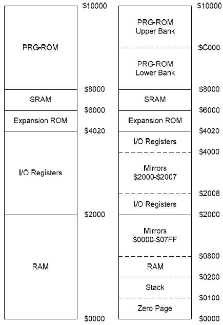
If you look at the values on
the right, you see many sections of the memory which are indicated as
"Mirrors." These addresses literally mean that using lower bit
wraparounds (i.e. higher bits are no connect), these addresses actually refer
to lower memory values. If we count out the mirrored values, then we will
note that the memory really only exists in a two sections: 2K for RAM
(Stack and Zero Page included) and a large section of memory contained on the
cartridge itself (Save RAM, Expansion RAM, and Program Rom). Since the cartridge
is intended to be fully self-contained, all we need to worry about is the 2K of
internal RAM, which easily fits inside of 4K of RAM included on the
Atmega644. Therefore, the easy solution to the memory issue is to
allocate 2K worth of NES memory on the heap (keeping space between the
emulation variables and the memory just in case something goes very wrong
involving the memory).
From here, whenever a call to
memory is made, we call a function (inlined, of course) which will make a few
address checks. First we check if the address is within the bounds of the
cartridge, and if so we set the out ports to the desired address, and await the
value on the data pin on the next cycle.
If the address is not above
the cartridge threshold ($4020), then we move ahead to check if we have an I/O
register. The first I/O register check is a direct check against the
$4000 - $4017 addresses. Reading or writing to each of these registers
has slightly different behavior, but in general the written values are stored
into the IO_register array and read out later. These values are synced up
with other hardware during writes by means of a two byte SPI protocol.
First, the lower byte of the address is sent, and upon completion of that
transmission, the new value to be written is sent. Since we have multiple
destinations for the SPI commands, the lower byte will never conflict on the
given hardware. The same idea applies to the $2000-$2007 addresses,
except that here we need to worry about the mirrored memory, and therefore we look
up the value of our array by means of a bitwise AND on the address to obtain
the zero to seven index we need into the PPU_register array.
All other addresses correspond
to an address of NES memory. These addresses are once again subject to a
bitwise AND in order to obtain the lower $7FF of the address as the index into
our memory allocation. Notice, that the emulation, nor the 6502 prevents
the user from accessing any value of the memory, stack included, meaning that
the stack itself is a completely viable set of memory.
Getting back to the SPI synchronization,
some of the I/O registers require special attention and care to certain
details. For example, since we were not emulating the audio systems, we
only store the values of the audio registers, but do not bother to sync them
via SPI across to other hardware (If we were to have done audio, it would have
been included on the controller polling circuit, which can be seen
below). In fact, only three registers in the $4000+ range actually matter
to this project. Two of these are the $4016 and $4017 registers which
pertain to controller reading, and the other is $4014, which is the sprite
direct memory access register.
The controller addresses have
extremely specific methods in which they need to be dealt with. Writing
any value whatsoever to $4016, initializes a controller poll for both
controllers. In our case the controllers are polled constantly and a
write to $4016 will simply entail an SPI synchronization of the two controller
states. Reads from the controllers are returned only in a bit at a time
on the NES. The low bit of $4016 and $4017 corresponds to an active low
signal for a button press. In order to obtain readings from all buttons
of the controller one must read the low bit 8 times, once for each button, as
immediately after reading a bit, the next value is shifted in from an external
shift register. The button order is A, B, Select, Start, Up, Down, Left,
and Right. The upper bits of the controller registers correspond to
functions that this emulation was not going to cover (i.e. "NES
Zapper" light gun). Since we do not support the values in those
upper bits, we simply send the polled values from the controllers, in flipped
order, such that after a read from the low bit of the controller, we will
simply shift the value right by one and overwrite the old value.
The details that are important
regarding sprite memory transfer to the PPU pertain to I/O registers $2003,
$2004, and $4014. These registers are some of the most important values
of the NES system. Use of these registers enables the cpu to access
Sprite RAM, which essentially is how movement is created across the
screen. Sprite RAM is a 256 byte memory bank that is internal to the
NES. The value in $2003 is the address that will be written to on the
next write. Register $2004 allows reading and writing from the address in
$2003. A write to Sprite RAM via this port will also cause an
post-increment of the address in $2003, but reads do not have any effect on this.
Register $4014 is an extremely
special register that dramatically increases the speed of the memory
transfers. Essentially, when you write a value into $4014, that value is
used as the upper byte of an address in the cpu memory space (cartridge or
internal), and memory is copied at a rate of two cycles per byte from cpu
memory (starting at the specified address) into Sprite RAM on the PPU starting
at the value indicated at $2003. This process is crucial because it
allows the transfer of a full set of new sprites to the PPU while only
requiring one action from the 6502 and only needing 512 cycles worth of
time. This allows the 6502 to continue with other work so long as it
keeps the data bus clear (meaning it can only use internal memory for 512 cycles).
Also, $4014 will only be written to during a period where the video is
disabled. This enables the PPU to wait to complete the entire memory
transfer, and to forget about synchronizing the screen. In order to
emulate this "hands off" process with Atmega644, we start by sending
the first byte of data via SPI and then set a counter to 255, which is the
number of bytes remaining to be transferred. Immediately before pooling
for the next instruction, the length of this variable is checked to see if it
is greater than zero. If so, the next byte is sent, but we do not wait
for the completion flags because we know that by the time we finish the next
instruction enough time will have passed. Each SPI write decremented such
that when it reaches zero, all of Sprite RAM will have been written. As
one would expect, the address in $2003 is incremented as each step in this
process is completed (this would be done by the PPU, not the 6502).
The 6502 is also entitled to
write to Video RAM by use of the $2005, $2006, and $2007 registers.
Writing to Video RAM is also restricted only to times of blanking for the
video, but does not require that the screen be disabled. In fact, nearly
all games use a version of writing to these registers during a horizontal
blanking in order to produce split-screen scrolling affects (more on scrolling
in the PPU section). The true functions of each of these registers is
more applicable to the PPU's workload, and will be discussed at that point.
The remaining registers are
$2000-$2002. The first two allow the 6502 to write certain information
regarding video specifics to the PPU. The most important thing that must
be noted of these two registers as far as the 6502 is concerned is the 7th bit
of $2000. Setting this bit to 1 enables the generation of Vertical
Blanking Interrupts, which are known as Non-Maskable Interrupts (NMIs).
These interrupts, unlike Interrupt Requests(IRQs), are not prevented by setting
the Interrupt Disable bit in the Status Register. Therefore, the only way
to stop the PPU from sending interrupt signals every time there is vertical
blanking is to set this bit to zero. This is handled in emulation immediately
before we grab a new instruction. Essentially, if this bit is set, and an
external pin is reading low (the blanking signal from the ELM304) then we push
the Status and PC onto the stack and jump to the address stored in memory at
($FFFB..$FFFA). We then execute the code located in the interrupt and at
the end of the interrupt, the last instruction it will execute will be the
Return From Interrupt(RTI) Instruction, which will pull the PC and the status
off of the stack and resume operation at the prior location (IRQs will jump to
the address at ($FFFD..$FFFC), and Break Commands, which are generated by software,
will jump to ($FFFF..$FFFE)).
Picture Processing Unit (PPU)
While
we were unable to create a PPU that could run in real-time with the 6502, we
still managed to process a subtle video program which works in ways that are
identical to those of the PPU. First, however I will discuss the data
available to the PPU and the methods it utilizes in creating video.
In general, the PPU processes
a 32 character wide, 30 character high screen, where each character is an 8x8
block of pixels. It has a color palette that supports 64 colors (9 of
which are infinitesimally different shades of black), however can only have 25
onscreen at any given time. It supports a full background of screen and
additionally supports up to 64 sprites (with a maximum of 8 per scanline).
The PPU is heavily dependent on multiple sources of incoming memory:
Each of the elements contained within memory has a very specific and pertinent
purpose.
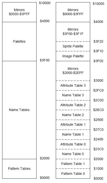
Pattern
Tables -
The Pattern Tables contain the
defining bitmaps for the individual characters of video. Each pattern
table ($0000, $1000), contains memory for 256 characters, each requiring 16
bytes of memory. The first 8 and second 8 serve a slightly different
purpose. Each bit of the first 8 bytes (total of 64 bits), corresponds to
the 0 bit of the color palette selection for that pixel, and the second 8 bytes
similarly define the 1 bit of the palette selection. One table is
designed for use as background tiles, the other is defined for use by the
sprite tiles (This is indicated by a bit in the $2000 I/O register).
Combinations of the these bits that produce a zero offset are considered
transparent
Name
Tables / Attribute Tables -
Each of the four name tables
is a 960 byte area that essentially stores the 960 characters that make up the
background of the screen. This data is stored in the form of indexes that
offset into the pattern tables by increments of 16. Each name table has a
corresponding attribute table. The attribute tables contain 64 bytes,
with each byte storing the bits 2 and 3 of the palette color selection for
pixels. Each individual byte is mapped to a 4x4 character selection, and
each two bits of this byte are further divided to be used for 2x2
sections. (Attribute bytes are one of the more complicated things to
understand about the PPU, and therefore I direct those interested to the NES
references at the end of this document.) All of these values are filled
by the 6502 during blanking moments of the frame. The memory map states
that there are 4 name tables and attribute tables, however the NES only has
enough memory to store 2. Therefore, it is quite common to have 2 of the
tables map back to 2 others. Some cartridges provide additional RAM in
order to have enough memory for them. In order to produce these
mirrorings of name tables, address lines from Video RAM are routed through the
cartridge and pack to the PPU such that the cartridge can internally change the
state of address bit 10 and/or 11 as deemed necessary.
Image /
Sprite Palette -
The palettes define the 25
colors that will be on screen at any given time. These values can be
changed by the 6502 by writing to Video RAM through the I/O Registers.
These palettes are the values that get indexed to by the resulting values of
combining the pattern tables, attribute tables, and name tables. Also, it
should be noted that the value at palette entry 0 is the background color and
is so important that it is mirrored every 4 bytes such that
"transparent" pixels can be used no matter what the attribute table
memory has stored.
Video
Scrolling -
Video Scrolling is done by
means of $2006 and $2005. These registers take on different purposes
during the frame because the NES intentionally uses them internally as the
offset in the name tables. Essentially, every time a screen is started,
an initial byte value in the name tables will be specified, along with an
addition bit offset, which determines exactly where the screen starts and
ends. In addition to this, as you draw pixels across the screen it is
almost inevitable that you will cross one name table onto the other. It
is by the use of different name tables that the screen is scrolled, because at
any given time, you will be writing the contents to a certain value of the name
table memory which is considered an off screen portion, and as the video wraps
around the name tables, over and over again, you will continually draw the
contents of the screen to come about half a screen before it is actually
displayed.
The demo program that we have
included on this page, has values hard-coded into it that define the sprite
character of Mario from the original Super Mario Brothers game. The data
for the sprite was obtained by extracting data from the pattern tables using a
program designed to solely read from a cartridge. We defined the four
colors which we knew Mario to be made of and simply ran pattern table after
pattern table until we found the tiles that we needed. These tiles were
not too hard to find because once one was found, all of the others were quite
local. We then go ahead and calculate the image in the exact same way
that an the sprite would have been processed by the NES PPU.
The software that generated
video used an external pin interrupt on the rising edge from the ELM 304.
To make sure that we entered the interrupt with consistency, we slept the CPU
in main such that only the interrupt could awaken it. Once in the
interrupt, we checked if the ELM was outputting white raster, or if it was in a
blanking stage. If it was in white raster, then we went ahead and pushed
pixels out onto the screen. If it was blanking stage then we set the line
counter to zero and returned.
Drawing pixels onto the screen
using the AD724 requires an AC-coupled signal. To produce this, we would
alternate our signal to DAC between the color pixel that we wanted to display
and zeroes. Doing so essentially modeled an AC signal and produced the
expected output color. The color pixels that we implemented occupied an
entire byte and were composed of 3 red, 3 green, and 2 blue bits, which were
all passed into a DAC. To make the screen a total of only 16 x 16
pixels. First we would draw the same color onto the screen for 16
consecutive pixels rather than just one and secondly, we used every 16 lines as
an offset into our image, meaning that line shifted right by 5 produced the
pointer to the memory we wanted to use as our 16 byte line. Selection
between images to create motion was done using a timer which incremented every
time we entered the interrupt. After about 1000 counts of the counter, we
would increment to the next image, and reset the counter.
The reason that we could not
complete a full emulation of the PPU is strictly a timing issue.
Extracting data from the pattern tables is a task that simply cannot be done
without additional hardware or a faster CPU. The NES natively makes 170
memory accesses during a single scanline. Making these accesses is not
the bottleneck that prevented us from continuing, because when we run at 20MHz,
we have enough time to execute just over 1200 cycles per scanline. The
real issue is just figuring out what each pixel needs to be and storing a full
256 x 240 pixels (64Kbytes) onto external memory.
HARDWARE
The
hardware in this lab is fairly complex, but relatively straightforward.
There are three different MCUs involved, the NES Cartridge, external RAM, and a
couple of video outputting chips. We have had several different circuit
configurations throughout this project. In our final version, we have
circuits for the individual parts, and one complete circuit for the entire
system. Unfortunately, we were never able to complete the full product,
so the final circuit was never assembled, but the schematics for it are
attached in the appendix. Below, we will step through the various
circuits, how they are assembled, and the theory behind their design.
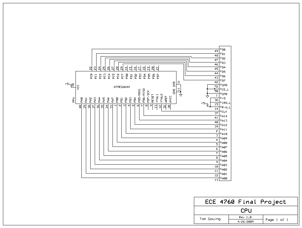
CPU
The
CPU code needs to interface with the NES Cartridge. We bought a 72-pin
connector from www.electronicsurplus.com to interface with the cartridge.
This way we could solder connections to the various pins. Our original
approach was to just use an original NES connector, but we found it far too
bulky and we didn't want to solder onto it because we didn't want to ruin
it. We got a pinot of the cartridge
(http://benheck.com/Downloads/NES_Famicom_Pinouts.pdf) so that we knew which
pins interfaced to specific parts of the game. For the CPU portion of our
project, we chose to read from the Program Memory on the cartridge, and execute
the instructions. The hardware here is very straightforward, we just
needed to connect all the signals necessary to access the Program Memory.
This would include pins 1-15 and 37-50. We wired these up to the various
ports on the MCU, so that we could manipulate them as necessary.
For this circuit, we used a
large solder board. We soldered in the 72-pin connector, and the
appropriate wires. Then we jumped these wires over to the protoboard, and
soldered them into the preferred ports. The address takes up two ports, the
data only one port, and the various other signals are on the fourth port.
It doesn't matter which port is which, just whatever is easiest to wire.
We had originally tried wiring this circuit on a breadboard, but it quickly
turned into an unstable rats nest, so we had to solder it down.
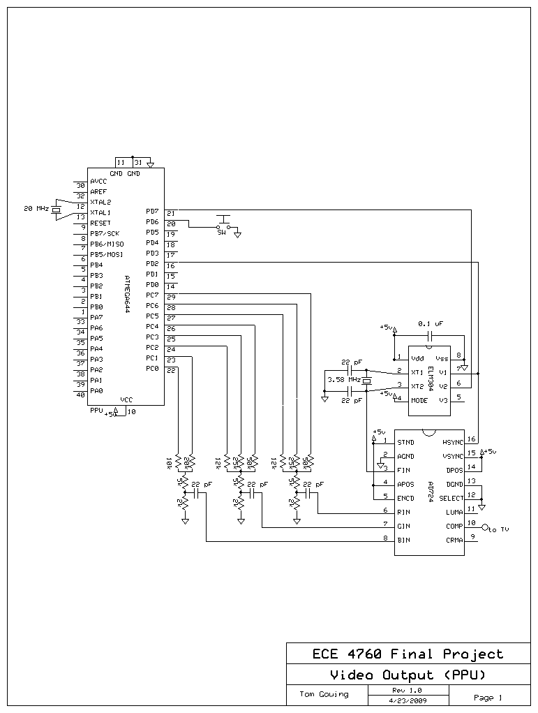
PPU / Video Output
The
emulation of the PPU was probably the most difficult part of our project.
There is some good documentation on the web, but not as much as for the
CPU. The major issue that we ran into with the PPU is that it is too
specialized. This made it near impossible to emulate the PPU entirely in
software. The NES has other hardware in the system with likely off loads
some of the work. To be able to do this all in software, we would need a
significantly faster clock than the AtMega644 can handle. If we had more
time, we may have been able to make more progress on the PPU, but in merely 5-6
weeks, we couldn't completely emulate it.
So what we decided to do was
show an example of decoding some sprites, and display them on the screen.
Using software, we set up the screen so that it was a 16x16 grid. Sprites
are 8x8, and most characters are made up of either 4 or 8 sprites. We
could only display characters of 4 sprites, so we chose to display small Mario,
from Super Mario Brothers. Our program shows Mario standing still, then
he starts running to the right. We have set up a push-button which will
tell Mario to change directions. There are 10 different screens involved
in this animation. There is a set of 4 sprites for each of the following
screens: standing facing right, 3 for running to the right, and 1 for turning
from right to left. We take the same 5 frames from before and decode them
differently to obtain the flipped versions, so that he may run in the other
direction.
The Hardware consists of a few
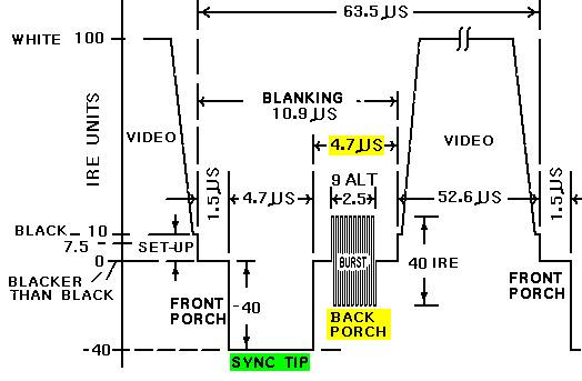
specialized chips to help us generate a color NTSC signal. First of all,
there is the ELM 304, we use this chip to generate our SYNC pulses, and to tell
us when to write the screen. We run the ELM304 in "100% White"
mode. This way if V1 and V2 are high, we know that we are in the visible
screen. We can also use the V1 signal as our SYNC pulse to send to the
AD724.
The AD724 is a RGB to NTSC
converter. This takes in three color inputs, one for each of Red, Green,
and Blue. Through these three inputs we can make various colors.
The output is a pure NTSC color signal, which we send through a 75 Ohm resistor
to the TV. We send the color data to the AD724 directly from the Microcontroller.
This is through a DAC to bring our 5V output down to an acceptable level of
714mV peak to peak. The input must be AC, which we accomplish by rapidly
changing the input between 5V and 0V, then passing through the DAC. We
use a capacitor to remove the AC-couple the signal. Much of this hardware
is very similar to previous 476 projects, specifically we took a large amount
of information from a Project from 2006, "Higher resolution TV" by
Keith Jamison and Morgan Winer.
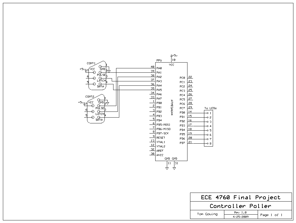
Controller Polling
The circuit
for controller polling is fairly simple. We have two controller
connectors which we purchased from parallax
(http://www.parallax.com/Store/Components/Other/tabid/157/CategoryID/32/List/0/SortField/0/Level/a/ProductID/522/Default.aspx).
We found the controller pinot various places on the Internet, and connected
wires to the 5 pins that are used. The 5 lines are Vcc, Ground, Pulse,
Latch, and Data. We cut two sockets out of an old piece of PCB to hold
the two connectors in place, so that they would be kept stable. We used
hot glue to secure all the physical connections, so that nothing could get
dislodged due to transport.
We have the controllers wired
up to PINA on an AtMega644, each taking three pins. The software sends various
signals to the controller to poll for its contents. First, we send a
signal on the "latch" line to the controller telling it to latch its
current state. Then we send 8 clock pulses on the "pulse" line,
initially high, and when they toggle to the low state the controller pushes out
a bit on the data line. The data from the controller is combined into one
byte, one bit for each button, active low. Then we can display on the
LEDs the status of the various buttons, so that the user can see a response
when they interact with the controller. To effectively use the controller
with the rest of our system, we would interface via SPI. Using SPI we can
display the status LEDs on an STK500, while running our controller code on a
protoboard.
RESULTS
For
the most part, all of our circuits lived up to their expectations.
Everything executes with a good speed. The only circuit that we've had
performance issues with is the video output circuit. The Video executes
quickly enough, but it has some visual artifacts. We could generate a
fast screen that had no artifacts if we did an 8x8 grid. When we extended
it to a 16x16 grid, we had to only worry about speed, so the visual quality
went down a bit. We have visible lines vertically on the screen, between
pixels.
There
were no safety issues to worry about with our design. Nothing about our
project is easily harmful to anyone. Our design also doesn't interfere
with any other systems. There is nothing about our project that should
have usability issues. The controller is fairly standard, and the only
other user input is a push button for the video code.
CONCLUSION
Design Analysis
The major failure of our
project was that we were unable to create an entire NES, which was our initial
goal. All along we knew that this was a lofty goal, and that many people
have tried it in the past and failed. For some reason we still held on to
the hopes that we could do it. Early on, it truly looked like we would be
able to pull it off, the CPU code came together well, and we successfully read
the cartridge on the first try. Unfortunately this luck didn't last long
enough. We tried emulating the PPU in a couple of different ways, and
after each change we thought the new design would work, but it never did.
Emulating the PPU was just too difficult. If anyone reads this hoping to
make a NES, I strongly suggest that you focus on the PPU alone, and use our
code as a reference for everything else. I hope that sometime someone can
complete the entire system for a final project.
NTSC Standard
Our
design needed to output NTSC video signal to a Color TV. We achieved this by using the AD724 RGB to
NTSC converter. We also had an ELM304
for our sync pulse generation. These two
working together, created our NTSC signal.
This way we knew that we would conform to the standard.
Intellectual
Property
We used reference code and
discussion from previous projects: Higher Resolution Color TV by Keith
Jamison and Morgan Winer, and Apple II Emulator by Brian Rudo and Tyler
Orchowski. No code from the public domain was used, and therefore no Open
Source license agreements exist. Since our project was a recreation of
the system created by Nintendo, we needed to be sure that we did not break any
copyrights. In order to minimize the chances, we decided that using the
cartridges would be a sufficient way to ensure that no copyrights were broken,
because we would not be running ROM files, which would be pirated software. We
did not need to sign any Non-Disclosure agreements for the samples we were
given. There are no patent or publishing opportunities.
Ethical
Concerns
For this project, we kept the
ethical considerations close at mind while working. Our project,
contained minimal presence of danger to any user at any time. The most
dangerous piece of our project was the power supply, which was quite well
contained and it would be almost impossible for it to harm anyone. After
being in lab and working on our own project for so long, it is quite natural
for us to find interest in other groups projects. There were many times
where I would go ask others what they were doing and what problems they had
been running into, and if I had any clue on the topic that they were having
issues with, we would try and give them as much advice as possible. All
of the projects are extremely interesting and often from discussing ideas for
algorithms and implementations with others, we gained invaluable insight into
our own efforts. In our time in lab, we never made any decisions that
would put the groups around us at risk in lab.
That being said, I don't think we would really do anything differently.
It was fun to try and make a NES, and while we were unable to complete our
goal, it was fun to attempt it.
Commented Code:
ColorVid.c
(20 MHz crystal)
mario.h
cpu6502.c
cpu6502.h
SPI_MASTER_TEST.c
NESController.c
NESController.h
Budget:
|
Item |
Cost |
Vendor |
Part # |
|
STK500 |
$15 |
N/A |
N/A |
|
72-pin connector |
$2 |
Electronic Surplus |
72-pin Edge Card Connector 0.1” |
|
AD724 |
Sample |
Analog Devices |
AD724 |
|
ELM304 |
$6.50 |
ELM |
ELM304 |
|
UART Cable |
$1 |
N/A |
N/A |
|
2 Breadboards |
1 Free, 1 $6 |
N/A |
N/A |
|
Large Solder Board |
Free |
N/A |
N/A |
|
3 Crystals |
$3 |
N/A |
N/A |
|
Resistors, Caps, etc. |
Free in lab |
N/A |
N/A |
|
Lots of Wire |
Free |
N/A |
N/A |
|
Protoboard |
$4 |
N/A |
N/A |
|
Color TV |
Free (previously owned) |
N/A |
N/A |
|
NES Controller |
Free (previously owned) |
N/A |
N/A |
|
Power Supply |
$5 |
N/A |
N/A |
|
1 MCU Socket |
$0.50 |
N/A |
N/A |
|
5 Machine Pins |
$0.25 |
N/A |
N/A |
|
2 Controller Sockets |
$4 |
Parallax |
NES Controller Socket |
|
SOIC pad |
$1 |
N/A |
N/A |
|
2 AtMega644’s |
Free Sample |
AtMega |
|
|
|
|
|
|
|
Total |
$48.25 |
N/A |
N/A |
Tasks:
6502 Code – Brian
Cartridge Hardware – Tom
Controller Polling/SPI Code – Brian
Controller Hardware – Tom
Video Output Code – Tom & Brian
Video Output Hardware – Tom & Brian
References:
Higher Resolution Color TV by Keith
Jamison and Morgan Winer
Apple II Emulator by Brian Rudo and Tyler
Orchowski
6502 Instructions
6502 Instruction Set
NES Specifications
Nintendo Entertainment
System Documentation
NES
PPU
Data Sheets
ELM304
- NTSC Signal Generator
AD724 - RGB to NTSC Video Converter
DS1245AB - Non-volatile RAM (Chip not used in final design)