ATmega644 JTAG Debugger
ECE 4760 Final Project by Jasper Schneider(jgs33) and Rui Rick Wu (rrw32)
Introduction
The purpose of this project was to design and implement a debugger for the ATmega644 that communicated through its JTAG interface and was capable of controlling program execution by setting breakpoints and accessing registers and memory.
We have three main objectives in this report:
- To enable a user to properly download our code onto an ATmega644, connect and configure a target, and begin debugging. See our User Guide.
- To serve as documentation on the On-Chip Debugger for the ATmega family of MCUs. See the OCD Documentation.
- To detail how we structured and designed the debugger from the very bottom level (serial bit input) to upper level commands (i.e. memory reads). See Design Schematics and Overview.
High Level Design
Rationale
During our time in ECE 4760, we encountered situations in which our code did not function as expected. We found debugging with print statements to HyperTerminal and flashing LEDs to be both insufficient and occasionally unsafe. Thus, it would be very helpful to have a debugger for the ATmega644 that we could use to set breakpoints and step through our program with access to memory and registers. Such devices are often very expensive. Even the JTAG ICE mkII, which Atmel labels a low-cost debugging tool, is sold for approximately $300. Our project attempted to build a debugger for an ATmega644 using a second microcontroller that communicated with the target board via the JTAG interface. We hoped to emulate the basic functionality of the JTAG ICE mkII, with features such as setting breakpoints, reading and writing data registers, I/O registers, and memory, and single stepping.
Design Schematic and Overview
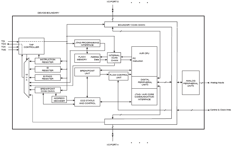
Our project consists of two ATmega644 MCUs. The microcontroller that we are debugging (referred to as the target) is programmed by the user with any arbitrary code. The other microcontroller (the debugger) contains the actual debugging firmware. The user is able to interface with the debugger through a command window on HyperTerminal. The debugging MCU is then able to control the target via the JTAG port. Our code running on the debugger sends a series of bits to the JTAG interface, which then stores it in the instruction / data registers of the JTAG. The JTAG interface is described in detail in the next section. The JTAG interface alone however does not allow us to perform all the necessary functions of our debugger. The ATmega644 contains an On-Chip Debugger unit, which is the module that can actually execute AVR instructions and set breakpoints.
We begin by describing the JTAG and OCD modules, including their respective registers, instruction sets, and communication protocols. Next, we discuss the design of our hardware and software, including an API describing each user function. Finally we discuss the results of our project.
Basic JTAG Overview
This project makes use of IEEE standard 1149.1, entitled Standard Test Access Port and Boundary-Scan Architecture. This standard was written by the Joint Test Action Group and is commonly referred to as JTAG. JTAG is commonly used to debug embedded systems and to program hardware devices. Companies like Atmel often provide JTAG interfaces on their products because of its popularity in industry. The ATmega644 comes with an On-Chip Debugger and an IEEE 1149.1 compliant JTAG interface.
The JTAG standard uses four signals: TCK, TMS, TDI, and TDO. TCK is a clock signal. TMS is the Test Mode Select signal which is used to navigate the JTAG state machine (See JTAG State Machine). TDI is the Test Data Input signal used to provide input for the JTAG interface. TDO is the Test Data Output signal used to retrieve the output data from the JTAG interface. These four signals are accessed through four port pins on the ATmega644 that are called the Test Access Port when using JTAG. Port pin C.2 is used for TCK, C.3 is used for TMS, C.4 is used for TDO, and C.5 is used for TDI. In order to use the Test Access Port, the JTAGEN fuse on the ATmega644 must be enabled. The IEEE standard also specifies a TRST signal, Test Reset, but this is an optional signal that is not used by the ATmega644.
JTAG State Machine
The JTAG standard is an implementation of the following state machine:
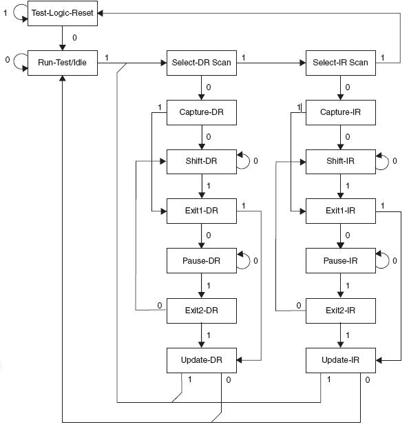
State transitions are controlled by the TMS signal, which is captured on the rising edge of TCK. The JTAG standard uses an Instruction Register, the contents of which determine the command to execute and which register to use as the Data Register. For example, if our IR content was 0x0, corresponding to the EXTEST instruction (See JTAG Instructions), then the multiplexer in the state machine would select the boundary scan chain register as the DR we would then shift data into. Likewise, if we wanted to access the OCD registers, we would first pass 0x08 into the instruction register. This would then select the Breakpoint Scan Chain as the DR.
To write to the Instruction Register, one must first navigate to the Shift-IR state. In this state, the TDI signal is captured on the rising edge of TCK and shifted into the Instruction Register. Data is shifted in one bit at a time, LSB first. TMS must remain 0 on the rising edge of TCK to stay in this state. When TMS is set to 1, it indicates that the MSB of the TDI data stream is being shifted in, and the Shift-IR state is exited. While shifting data into the Instruction Register, the data that was in the register, captured in the Capture-IR state, is shifted out to TDO, one bit at a time, on the falling edge of TCK. Reading from and writing to the selected Data Register can be accomplished the same way in the analogous DR states.
The Exit1, Pause, and Exit2 states are primarily used for state machine navigation. These can also be used to segment the data to shift in if there is not enough memory to shift one burst of data while in one of the Shift states.
The Update-IR state latches the instruction previously shifted into the Instruction Register on the falling edge of TCK. Once latched, the mode of operation is changed appropriately, including the selection of the appropriate Data Register. In the Update-DR state, the shifted in data is latched on the falling edge of TCK for registers with a latched parallel output.
The Run-Test/Idle state can be used as an idle state, and all of the methods we wrote returned the state machine to this state. There are certain testing instructions that can only be run in this state.
The Test-Logic-Reset state disables test logic and initializes the Instruction Register to contain the IDCODE instruction (See JTAG Instructions). Regardless of the current state, the Test-Logic-Reset state can be reached with five consecutive ones on TMS.
JTAG Instructions
To execute a JTAG instruction, a unique four bit code must be shifted into the Instruction Register. The following is a description of each instruction with its matching four bit code:
- IEEE 1149.1 Standard JTAG Instructions
- EXTEST 0x0: This instruction is used to perform a boundary scan. The Boundary-scan Chain is selected as the Data Register. On the ATmega644, performing a boundary scan returns the values of all port pins and their control bits.
- IDCODE 0x1: This instruction reports a version number, device number, and manufacturer code. The ID-Register is chosen as the Data Register.
- SAMPLE_PRELOAD 0x2: This instruction is used to pre-load the output latches and to take a snapshot of the I/O port pins without affecting system operations. This instruction is usually executed before executing the EXTEST instruction, since the EXTEST instruction will drive out the contents of the latched outputs of the Boundary-scan chain as soon as the EXTEST instruction is loaded.
- BYPASS 0xF: This instruction bypasses the boundary scan and simply sends the data shifted in from TDI directly out to TDO. The Bypass Register is chosen as the Data Register.
- AVR_RESET 0xC: This instruction forces an AVR device into Reset mode. The single bit Reset Register is selected as the Data Register. If there is a 1 in the Reset Chain, the reset will remain active. When a 0 is shifted in, the AVR device will exit Reset mode and restart program execution.
- AVR Specific JTAG Instruction:
On-Chip Debugger
The ATmega644 contains an On-Chip Debugger (OCD) that consists of a scan chain and a Breakpoint Unit, and it is capable of communication between the CPU and JTAG interface. The On-Chip Debugger was essential to the successful implementation of our debugger. The OCD contained the registers which configured and set the various breakpoints (described below). Also included was the On Chip Debugger Readback (OCDR) Register; this was the only IO Register belonging to the target board that the debugger could access through the JTAG port. Thus, with the OCDR, any register or memory location on the target board could be written to the OCDR, which the debugger could then read back.
It is important to note that the functions and registers of the OCD are all proprietary, and all original documentation is available only within Atmel. However, without knowledge of how to use the functions of the OCD, our project would have been impossible. We were able to find some documentation written by members of the Open Source community who had worked on creating a JTAG ICE mkII clone for the ATmega16. This documentation, although largely reliable, did have some inconsistencies with what we observed in our use of the OCD Registers. It is possible that this discrepancy could be due to differences between the ATmega16 and the ATmega644. We document below what we believe are the control and status bits of the On Chip Debugger registers for the ATmega644.
Description of OCD Registers
The OCD uses 16 16-bit registers. The On-Chip Debug Register (OCDR), OCD register 12, is used to provide communication between the CPU and JTAG interface. The other registers are listed below:
- 0 PSB0: This register is used to store a PC value to break on. The EN_PSB0 flag in the Break Control Register must be enabled to break on the stored value.
- 1 PSB1: This register is used to store a PC value to break on. The EN_PSB1 flag in the Break Control Register must be enabled to break on the stored value.
- 2 PDMSB: This register can either be used to break on a PC value or to break on data access. If PDMSB is storing a PC value to break on, then the EN_PDMSB, PDMSB0, and PDMSB1 flags in the Break Control Register must be set. If PDMSB is storing the address in memory to break on access, then the EN_PDMSB and PDMSB1 flags in the Break Control Register must be set.
- 3 PDSB: This register can either be used to break on a PC value or to break on data access. If PDSB is storing a PC value to break on, then the EN_PDSB, PDSB0, and PDSB1 flags in the Break Control Register must be set. If PDSB is storing the address in memory to break on access, then the EN_PDSB and PDSB1 flags in the Break Control Register must be set.
- 8 Break Control Register: This register contains flags to configure the OCD to break in the ways listed above. This includes breaking on a PC value, breaking on memory access, and breaking on change in program flow. The flags are ordered as follows:
Bit Number Name Description 15 RUNTIMER Enable timers to run during a Break 14 PC24 Selects between reading PC+2 and PC+4 during a Break 13 EN_STEP Enable single stepping 12 EN_FLOW Enable break on change of program flow 11 EN_PSB0 Enable use of PSB0 for break on PC 10 EN_PSB1 Enable use of PSB1 for break on PC 9 BMASK Use a mask for break comparisons 8 EN_PDMSB Enable use of PDMSB for break on PC and memory access 7 EN_PDSB Enable use of PDSB for break on PC and memory access 6 PDMSB1 PDMSB mode select - Enable for PC and memory breaks 5 PDMSB0 PDMSB mode select - Enable for PC breaks, clear for memory breaks 4 PDSB1 PDSB mode select - Enable for PC and memory breaks 3 PDSB0 PDSB mode select - Enable for PC breaks, clear for memory breaks 2 BCR2 Unknown 1 BCR1 Always 0 (non-writeable) 0 BCR0 Always 0 (non-writeable)
- 9 Break Status Register: This register contains flags that describe if a breakpoint has occurred, and if so, what kind of breakpoint. The flags are ordered as follows:
Bit Number Name Description 15 BSR15 Unknown 14 BSR14 Unknown 13 BSR13 Unknown 12 BSR12 Unknown 11 BSR11 Unknown 10 BSR10 Unknown 9 BSR9 Unknown 8 STEPB Single step break 7 FLOWB Break on change in program flow 6 PSB0B Break on PSB0 5 PSB1B Break on PSB1 4 PDMSBB Break on PDSB 3 PDSBB Break on PMDSB 2 BSR2 Unknown 1 ForceB Break by Force Break OCD function 0 SoftB Software Break
- 12 OCDR Readback Register: The upper 8 bits of this register contain the value stored in OCDR. The bottom 8 bits are unused.
- 13 OCD Control and Status Register: Only the MSB in this register is used. When set, OCDR is enabled.
On-Chip Debugger Specific JTAG Instructions
The On-Chip Debugger uses 4 instructions that are considered to be private and are only distributed within Atmel. There are numerous open source projects in which people have reverse engineered these commands. We used documentation written by Antti Lukatz with the Free AVR ICE Project as a reference.
- Force Break 0x8: This instruction forces a breakpoint in the target board.
- Run 0x9: This instruction is used to resume program execution after a break.
- Execute AVR Instruction 0xA: This JTAG instruction can be used to execute an AVR Instruction. The opcode for the instruction must be shifted into the Data Register. See the AVR Instruction Set for a detailed description of instructions and opcodes.
- Access OCD Registers 0xB: This JTAG instruction is used to read from and write to one of the 16 registers used by the On-Chip Debugger. The register to access, a read/write flag, and a data stream must be shifted into the Data Register. For a read operation, we set the data stream to all zeros. For write operations, the data stream specified the data to write to the selected register.
Breakpoint Unit
The OCD has a Breakpoint Unit that can be used to configure breakpoints in the following ways:
- 4 single Program Memory Breakpoints:
Enable the PSB0, PSB1, PDSB0, PDSB1, PDMSB0, PDMSB1, EN_PDSB, EN_PDMSB, EN_PSB0, and EN_PSB1 flags in the Break Control Register. Store the 4 PC values to break on in PSB0, PSB1, PDSB, and PDMSB. - 3 single Program Memory Breakpoints + 1 single Data Memory Breakpoint:
Enable the PSB0, PSB1, PDSB0, PDSB1, PDMSB1, EN_PDSB, EN_PDMSB, EN_PSB0, and EN_PSB1 flags in the Break Control Register. Store the 3 PC values to break on in PSB0, PSB1, and PDSB. Store the memory address to break on access in PDMSB. - 2 single Program Memory Breakpoints + 2 single Data Memory Breakpoints:
Enable the PSB0, PSB1, PDSB1, PDMSB1, EN_PDSB, EN_PDMSB, EN_PSB0, and EN_PSB1 flags in the Break Control Register. Store the 2 PC values to break on in PSB0 and PSB1. Store the two memory addresses to break on access in PDMSB and PDSB. - 2 single Program Memory Breakpoints + 1 Program Memory Breakpoint with mask:
We did not attempt setting breakpoints with a mask. We assume the user would at least have to set the BMASK flag in the Break Control Register - 2 single Program Memory Breakpoints + 1 Data Memory Breakpoint with mask:
We did not attempt setting breakpoints with a mask. The user can set the BMASK flag in the Break Control Register using the wocd command, but we did not extensively test this.
The current documentation used these names PSB and PDMSB without explicitly stating what they stood for. We interpreted PSB as Program Set Break, PDSB as Program/Data Set Break, and PDMSB as Program/Data with Mask Set Break.
Additionally, the debugger can break on a change in program flow of the target board (breaks on interrupts, jumps, branches). To do this, the EN_FLOW flag must be set in the Break Control Register. The debugger can also single step through the target board's program. To do this, the EN_STEP flag in the Break Control Register must be enabled.
Breakpoints can be set either during the reset state before the target board begins execution or while the target board is halted (by a breakpoint or forced break). For information on what commands to use to actually set the breakpoints, refer to the OCD commands section of the API.
To verify that we did indeed break on the desired point, the readOCD(char reg) function, which can be called in the command prompt with rocd(9), will return the status of our program execution. From the BSR table above, we can determine which condition that our program broke on.
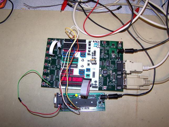
Hardware Design
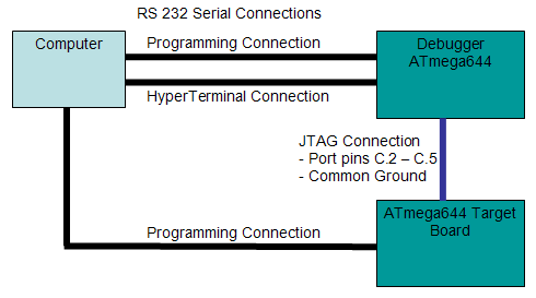
Our program required the use of two ATmega644s, one to act as the debugger, and the other to be the target board. The target board was mounted on an STK500. The JTAGEN and OCDEN fuses had to be enabled on this board for our debugger to be able to communicate with its JTAG pins and to access the On-Chip Debugger.
The other MCU was mounted on a prototype board for the ATmega32 and ATmega644. The specifications for this prototype board can be found at http://www.nbb.cornell.edu/neurobio/land/PROJECTS/Protoboard476/index.html. We soldered every component onto this board, including the RS232 driver socket and MAX233 chip. A serial connection was required with the debugger because user I/O was implemented with the UART via HyperTerminal.
The two boards shared a common ground, and their PORTC port pins were connected to allow for JTAG communication. Since the JTAGEN fuse was enabled on the target MCU, port pins C.2 through C.5 became the JTAG port pins. Specifically, C.2 becomes TCK, C.3 becomes TMS, C.4 becomes TDO, and C.5 becomes TDI. For ease in writing our program, we connected each necessary port pin to the corresponding port pin on the other MCU (i.e. C.2 was connected to C.2). On the debugger, port pins C.2, C.3, and C.5 were set to be output ports, while C.4 was set to be an input pin. This was because TCK, TMS, and TDI are JTAG inputs, while TDO is a JTAG output.
Software Design
Software Organization
Before writing our code, we divided the tasks that our debugger would need to perform into layers. The first two weeks of our project were spent at the low level; it was important to ensure that we had error free JTAG interface functions, as all higher level instructions would then build upon these. Next, after abstracting JTAG communication into two simple functions (DRSCAN and IRSCAN), we implemented useful assembly level instructions and On-Chip Debugger (OCD) instructions. Lastly, using series of assembly level instructions and OCD accesses, we created the high level functions such as the read/writing of memory. A complete set of all the functions are listed with descriptions in the API.
Low Level JTAG I/O
At the lowest level (JTAG I/O) were the methods to navigate the JTAG state machine. First, we wrote a method that performed a single state jump in the JTAG state machine, jtag_io. This method allows for synchronous communication with the target boards JTAG port in the following manner:
- PORTC.3 (Test Mode Select) and PORTC.5 (Test Data In) of the debugger are set to whatever value the user would like.
- _delay_us(1) is used to allow the value to meet setup time requirements.
- PORTC.2 (Clock) is set high, shifting the current value of TDI in.
- Another _delay_us(1) is used to meet hold time requirements.
- PORTC.2 (Clock) is set low, shifting out the current value of TDO (Test Data Out) on PORTC.4. We keep a global variable TDO_sreg (an unsigned long long) which can old up to 64 bits of shifted out data.
Thus, jtag_io allows for one bit to be shifted in and one bit to be shifted out. Next, using jtag_io as our basic unit of data transfer, we implemented DRSCAN and IRSCAN on top. These methods shift data in and out of the JTAG Data Registers (DR) and JTAG Instruction Register (IR). As mentioned above in the JTAG section, to run any instruction, the JTAG IR must first have an instruction shifted in. We based our jtag_io, IRSCAN, and DRSCAN methods on similar JTAG state machine navigation methods written by Altera. Altera's Jam STAPL freeware for JTAG programming and debugging can be found at https://www.altera.com/support/software/download/programming/jam/jam-index.jsp.
IRSCAN assumes that we are in the Run-Test/Idle state; this is a fair assumption as all IRSCAN and DRSCAN calls leave the state machine in the Run-Test/Idle state. Also, when the debugger is initialized, resetTMS() brings the JTAG state machine into the Run-Test Idle state by sending a series of 5 ones and one zero (this sequence will bring the state machine into the Run-Test/Idle state regardless of our current state). Each IRSCAN begins with a sequence of 4 jtag_io calls that bring the state machine into the Select-DR Scan > Select-IR Scan > Capture-IR > Shift-IR states. During these four jtag_io calls, the TDI does not matter because were traversing the state machine and not passing in any meaningful data. Once were in the Shift-IR state, we begin passing in our TDI array. While the data is being shifted in on the positive edge, the output will be shifted out on the negative edge. For IRSCAN, the output will not be meaningful to the user (it is not simply the instruction echoed out). The last bit shifted into the IR must be on the transition from the shift-IR state to the exit-IR state. After the instruction bits are shifted in, we run a series of jtag_io calls that brings the state machine from Exit1-IR > Pause-IR > Exit2-IR > Update-IR > Run-Test/Idle.
Some basic instructions require only a basic IRSCAN to perform the desired function (like force break and run). However, most require following up with a DRSCAN to initiate further instructions. Recall from the JTAG section that the IRSCAN allows the JTAG interface to automatically select the appropriate DR. DRSCAN works in a very similar manner as IRSCAN, except we enter Select-DR Scan > Capture-DR > Shift-DR. We stay in the Shift-DR for as long as 58 bits (for the EXTEST) instruction, and then exit to Exit1-DR > Pause-DR > Exit2-DR > Update-DR > Run-Test/Idle. Note that for read only operations, the TDI does not matter, so we elect to simply shift in a stream of zeroes; we care only about the TDO, which is shifted into the TDO_sreg variable of the debugger.
Note that both DRSCAN and IRSCAN take in as arguments the number of bits to be shifted in and a binary array of bits to be shifted in. This array is little endian, as we always start by shifting in the LSB into the JTAG. Thus, if we wanted to pass the instruction 0xC, our bit array would be {0,0,1,1}.
JTAG Commands
The next layer up is the JTAG command layer. This layer consists of the Boundary Scan JTAG instructions, as well as the four On-Chip Debugger specific JTAG instructions. Once the IRSCAN and DRSCAN instructions worked reliably, this level could be implemented by simply calling a series of IRSCAN and DRSCAN instructions. For example, forcing a break was done with IRSCAN(4, break_sequence). Execution of any arbitrary AVR assembler instruction could be done by using IRSCAN(4, avr_sequence) followed by a DRSCAN(16, assembler_opcode). JTAG commands such as run and break do not cause the program counter of the target boards program to be incremented.
On-Chip Debugger Commands
In this section we give a description of the important OCD functions, a brief overview of their implementations, and examples of their usage. For complete information on implementation, refer to the OCD section of the source code debugger.c. For those interested in solely the user interface of the OCD commands, refer to the API.
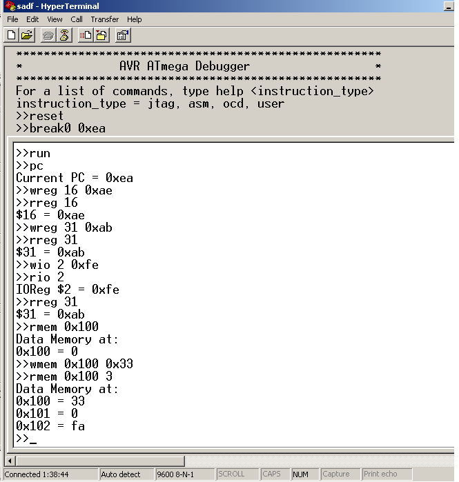
The OCD commands were especially critical in successful communication with the CPU as well as setting breakpoints. Our generic commands for the OCD are used to read and write the OCD registers. To write, we first call IRSCAN(4, {1,1,0,1}). Next, we call DRSCAN(21, TDI), where TDI is composed of {16bit value to write, 4 bit register location, 1 bit rw-flag}. For example, to write the value 0x400 to OCD Register 8 (this actually enables a breakpoint), the TDI would be {0000 0000 0010 0000 0001 1}. Reading the OCD is a bit more complicated. We must first latch the address of the register we are reading before we actually read. The read_OCDR method is implemented with the same IRSCAN(4, {1,1,0,1}), followed by a DRSCAN(5, latch_seq), and lastly a DRSCAN(21, TDI). The latch sequence consists of the register address followed by a zero (for the read-write flag). The TDI is the exact same as the write case, except with a one for the rw flag. The TDO will be captured on the DRSCAN(21, TDI). The rest of the OCD functions, written for user convenience, all call the writeOCD and readOCD functions to perform their tasks.
The read_OCDR() and enable_ocd() functions allow for the JTAG interface to communicate with the CPU, as it is the only register on the target we can access through the JTAG port. OCDR is mapped to I/O Register 0x31. Thus, if the target CPU can put the desired bytes into the OCDR, we can read it back. We discuss how to actually run instructions to perform register and memory transfers in the following assembly level section. For now, we are content reading back from OCDR. To first enable the use of the OCDR, we must first run the by writing 0x8000 into OCD Register D of the OCD. read_OCDR() then returns the value stored in OCD Register C, which is also I/O Reg 0x31.
In order to set a program break at PC value that the user found in the lss file of the target board program, we use the functions setPSB0, setPSB1, set_pPDMSB, or set_pPDSB. PSB0 and PSB1 are the standard breakpoint registers used exclusively for program breakpoints. Each of these functions work by writing the appropriate control bits to the BCR (Break Control Register), and then setting the corresponding register to the PC value we would like to break on. It is important to note that our breakpoint function will actually right shift the PC by 1. This is because the PCs contained in the lss file are incremented by +2 or +4, while the PCs kept in the CPU are +1 or +2. Thus, our breakpoint takes in the +2/+4 version and stores the +1/+2 into the PSB0/PSB1/PDSB/PDMSB registers. Refer to the API for the specific control bits that are set for each of the breakpoints.
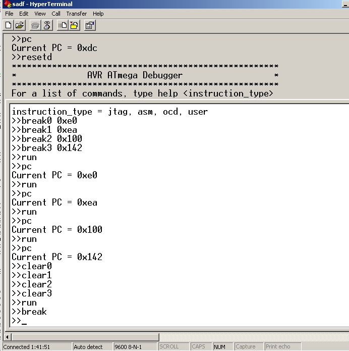
The user is given up to four hardware program breakpoints that can be set with break0, break1, break2, or break3 followed by the PC value. As mentioned above in the breakpoint unit section, we also have data breaks that use PDMSB and PDSB; these are set from the user interface by calling breakd0 or breakd1. When breakd0 is used as a data breakpoint, break2 will be removed as a program breakpoint. Similarly, when breakd1 is used, break3 will be cleared as a program breakpoint. These breakpoints can be cleared by using the clear[0-3] functions or cleard[0-1]. If we are currently at one of these breakpoints in the program execution, clearing the breakpoint will not resume execution. Rather, it will ensure that we do not break on it in the future.
Lastly, our program also includes the ability to single step and step through program flow. We start stepping or stepping through flow by typing in step or stepf. To resume standard execution without breaking on steps, the OCR must be cleared by typing in cstep or cflow.
Assembly Commands
The Assembly Function Layer consists of AVR instructions. These are primarily used for reading and writing memory, general purpose registers, and I/O registers, but other instructions were included to read the PC, perform jump operations, and to enable or disable interrupts in the target board.
All assembly functions required first an IRSCAN(4, {0,1,0,1} /*0xA*/). This selects execute AVR instruction as the execution mode. Next, we call DRSCAN(16, opcode) or DRSCAN(32,opcode), depending on whether opcode is a one or two word AVR instruction. Opcode is simply the little endian hex representation of any AVR assembly instruction. Although we did not specifically implement every single AVR instruction, it is possible for the user to execute any of them by calling the exec function, which takes as argument the opcode.
The reason we chose to implement only certain functions is the fact that assembly instructions come in many different formats that all require different parsing. For different instructions, the destination registers, source registers, and immediates were often in different locations of the opcode. Occasionally, the opcode could have a value that was spread through the opcode, such as LDI (with opcode 1110 KKKK dddd KKKK, where k = immediate and d = destination register). Thus, each of our functions simply took the immediate value (if applicable), destination PC, memory location, or destination / source registers, combined it appropriately into the appropriate opcode, and performed a DRSCAN (16, opcode).
Most of the commands we wrote in this section relate to memory and register transfers. However, there were some extra instructions that would be useful for a user. CLI and SEI can clear the interrupt enable or set an interrupt enable; thus, if the user felt like the interrupts were giving unstable behavior, they could be easily disabled during program execution. Also, we found an instruction undocumented in the AVR 8-bit instruction set for reading the current PC. This is run by giving an opcode of 0xFFFF0000. The PC is shifted out on TDO, which we then shift left by 1 to give a value that makes sense to the user.
High Level Commands
At the highest level, we wrote user commands which call a series of the above listed methods to perform the desired functionality.
The register reading and writing instructions are fairly simple. Writing simply loads a user specified character into a data register between 16 and 31. Reading sends the contents of the register we want to read into OCDR, which we then read back from the JTAG. Reading and writing of I/O ports is a bit more complicated. In order to actually write to an I/O, we first place our character into a data register via LDI. However, this will destroy whatever used to be in that particular data register. To solve this problem, it was necessary to make use of the stack to store our register values before we begin to manipulate them. save_context() and restore_context() are two helper functions that accomplish this. save_context() pushes the contents of data registers 26 31 on to the stack, and restore_context() pops them off after whatever instruction were running has completed. Registers 26 31 (X, Y, and Z registers) are saved because those are the only ones weve elected to use for temporary data storage. Returning to read/writing of I/O ports: after putting the character we want to write into register 31, we then run the out() function, which will output the contents of register 31 to a user specified I/O register. Reading works similarly, except for using in() instead of out().
We finally have enough functions now to read and write memory. Again, we will need to use save and restore contexts before and after our memory reading. Writing begins with loading the value we want to write into register 31. ST Store Indirect From Register to Data Space using Index X is then used to bring the value in register 31 into the user specified address. This address is stored with the high bytes into register 27 and the low into register 26 (these two registers comprise the X register). Similarly, reading makes use of the X register to store the memory value it wants to read from, reads it back to reg 31, and then sends it to OCDR where we can access the value.
Also included for the user were instructions for resetting the debugger as well as basic arithmetic operations. Resetting the debugger is done simply by simply jumping to PC = 0. The program will restart, going through the initialization. In the initialization of the debugger code are JTAG instructions which will bring the target board into the reset state, clear all breakpoints, and zero all the internal debugger state variables.
Lastly, the help commands will give a list of each of the functions available to the user under each section. A brief description of all the functions is also included.
API
Not all functions were mentioned in the above description, only those most commonly used. For a description of each method, organized by software layer, see the API.
UART
We used the UART for user input and printing output via HyperTerminal. We used the blocking fscanf command in our main method to read user input. The inputted string was parsed into a command name and any hexadecimal arguments, which were then used to call one of the user functions. The debugger did not need to perform any task until the user entered a command, so interrupt driven I/O with the UART was not needed.
Testing and Results
We tested our code as we added functions to it. When testing our code, we programmed the target board a modified version of the blinkyGCC644.c written by Bruce Land. In our version of the code, the initialization method contained a very rapid set of blinks to distinguish the beginning of the program from normal execution. We also added a variable called hello to test our memory functions, and we added instructions to modify PORTA to test some I/O register functions. We used the lss and map files generated for this code as reference for data addresses and PC values.
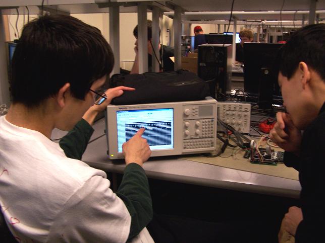
First, we tested the Force Break and Run commands, since they only required one pass of the IR chain of the JTAG state machine. These worked as expected, so we then moved on to accessing the OCD and performing AVR instructions. These required a pass through the IR chain first and then through the DR chain. From testing accessing of the OCD, we noticed that our DRSCAN was not returning to a safe state all the time. Initially, our break, run, and access OCD functions looped through long arrays of TDI and TMS sequences, and there was a lot of code duplication to navigate the state machine. It was somewhat difficult to follow, so we re-wrote our JTAG state machine navigation methods. We wrote our jtag_io single state transition method and our IRSCAN and DRSCAN methods. We ensured that IRSCAN and DRSCAN always ended in the Run-Test/Idle state. We then monitored our JTAG state machine navigations with a Logic Analyzer and verified that the JTAG signals on the TAP controller were behaving as expected.
We continued to work on our functions to access the OCD registers. We encountered difficulties reading the registers, and after studying the code written by Antti Lukatz, we discovered that we were not latching the address of the desired register before reading it. We modified our read functions to first latch the register address by calling DRSCAN with a five bit TDI stream, 4 bits for the address to latch and the one bit read/write flag. After latching the address in the Update-DR state, we were able to read from the desired register with a second call of DRSCAN.
After successful reading and writing of the OCD registers, we were still inexplicably unable to set breakpoints in a predictable manner. Eventually, we discovered that the bits in the Break Control Register (BCR) used to enable breakpoints were not functioning as expected. For our use, all the enable bits were shifted by one. We supposed that this difference was either due to an error in the documentation or difference between the ATmega16 and 644. This highlights an issue that troubled us throughout the course of the projectthe documentation was not only sparse, but at times difficult to understand. We oftentimes tried various interpretations of the only documentation we had, resulting in many hours of failure.
Another issue we encountered was timing between the debugger functions and the user I/O UART functions. We originally started the code with interrupt-driven I/O. We realized that this was not needed, since our debugger did not perform any tasks until the user entered a command. Since synchronization of tasks was not an issue, we switched our I/O to use the blocking fscanf function. Our program did not perform any tasks until the user entered a command, and there were no more timing issues with the UART.
When setting breakpoints, we had difficulties discovering which PC value to store in the PSB0 and PSB1 registers to get the appropriate breakpoints. We first tried entering the PC values listed on the lss file corresponding to the program running on the target board, but these did not work. The lss file only contained even PC values, while our readPC method returned even and odd values. The AVR instruction set said that the PC would be incremented by either 1 or 2 depending on the instruction, while the breakpoint documentation written by Lukatz said it could increment by either 2 or 4. We found that the PC values listed in the lss file were shifted left by one bit from the PC values used by the AVR instructions. The addition of either 2 or 4 was equivalent to an addition of either 1 or 2 after shifting. We modified our functions to shift the PC values appropriately so that the user could enter the PC values listed in the lss file.
Perhaps the greatest difficulty we encountered was in restoring PC values after execution of AVR Instructions and OCD Commands. We noticed that reading the PC during a break caused it to increment each time. Furthermore, we noticed that any AVR instruction we executed caused the PC to increment. This was a problem, since we could not resume program execution from where it left off when we entered the Run command. We originally tried to store the current PC in a variable, and then perform an ijump to this variable to restore it. This was not working as expected and different instructions seemed to cause different increments to the PC. We decided to change our approach to better handle some of the behavior we encountered. First, some AVR instructions are two word instructions that increment the PC twice. Some of our commands also depended on calling multiple AVR instructions, so we had to handle multiple PC increments. We decided that instead of saving the PC and restoring with ijump, we would simply use the rjmp instruction to put the PC back far enough to undo any PC increments and reach the current PC that we set the breakpoint on. The PC restore method we wrote took an argument that governed how many increments of the PC to undo based on the AVR instruction or instructions executed. This way, we could handle two word instructions and multiple instruction calls. Finally, we noticed that our OCD commands to read from and write to the OCD registers also caused the PC to increment. We tried restoring the PC with these methods as well, but this still did not seem to work all the time. It seemed as if reading a PC value immediately after an OCD command would return an incorrect PC value, but if we executed another instruction in between, the PC would return to normal. We decided to insert a two word nop in our OCD commands to take care of this. The insertion of these nops fixed the PC value read after performing OCD commands.
Even after our PC restoration appeared to be working, we could not get the break on change in program flow and single stepping to be completely reliable. Once the program had started running, we could start single stepping in our main method, and single steps appeared to work. If we instead started single stepping at the very beginning of program execution, single stepping would not get the program through its initializations and into its primary task.
We were never completely sure of the proper way to restore PC values. We could not find any documentation on the subject, but it was an issue that required a solution of some form. If the PC values were not restored, then executing a command like rreg that invoked multiple AVR instructions would increment the PC multiple times. If we resumed program execution without restoring the PC, then the target board would be left in an unsafe state, having skipped instructions and potentially missed branches or jumps. Having no reference documentation, we chose our solution because it appeared to work. The only cases when it was sometimes unreliable was when running the step and stepf commands.
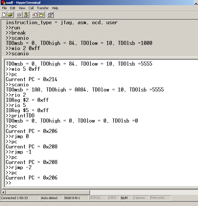
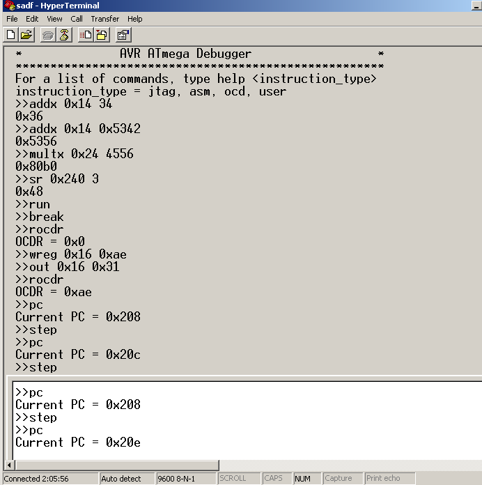
The following are some screenshots of the user interface on HyperTerminal with some sample instructions:
Conclusions
Meeting Expectations
Our finished product exceeded the expectations we had when we first started the project. Because none of the course staff had seen any project of this nature, our goal was simply to implement as many useful features of the debugger as possible. In the end, our debugger was able to perform nearly all the functions we had earlier envisioned. We created a debugger for the ATmega644 using a second ATmega644; the MCUs communicated through the JTAG interface on port pins C.2 - C.5 according to the IEEE 1149.1 JTAG Standard. Specifically, our debugger can set breakpoints at PC values, on memory access, on a change in program flow, or by a Force Break command. During a break, our debugger can read from and write to the target board's I/O registers, data registers, data memory, and OCD registers. The user can then resume program execution. The user communicates with the debugger via HyperTerminal, and we have provided an API of user commands that implement the debugger functionality.
One of our greatest challenges in proceeding with our project was our limited knowledge of the complete functionality of the debugger. There is not much existing documentation concerning the OCD, and the open source projects only provide limited documentation based on the contributor's findings. When we did not know the exact specifics of what a particular function was supposed to do, we made an educated guess based on our research and testing.
There is significant room for further improvements with this project. It would have been desirable to get break on change in program flow and single stepping to be completely reliable. Also, we would like to have complete access to EEPROM. This would have allowed us to implement an unlimited amount of software breakpoints, read the current instruction, and possibly even reprogram the code execution stream.
For completeness, we could also extend the API to include all AVR instructions. We wrote commands that only executed a subset of the instruction set that we found most relevant and useful to our project. We did provide the user the option of executing any AVR instruction if they deciphered the opcode on their own, but having simple one word or two word commands to enter into HyperTerminal would be much simpler. Finally, we would like to be able to set breakpoints with a mask for break comparisons. Using the lss and map files, the user can easily set breakpoints on actual PC values and memory addresses. Breaking with a mask does not seem necessary, but could be done for completeness.
Currently, our project is a standalone application which can plug into a target board and a computer and begin debugging immediately. This makes it considerably easier for the user to use; because AVR Studio is circumvented, no software installation or configuration is necessary. Nonetheless, it would still be extremely useful to actually make our debugger compatible with gdb. An existing interface known as AVaRICE provided by Atmel can be used to interface gdb with the debugger. Some work has been done in this area with the ATmega16 by Antti Lukatz and Armand ten Doesschate. We hope to continue working with our version for the ATmega644 and contribute to the open source AVR Debugger project.
Conformity with Standards
Our program was compliant with the IEEE 1149.1 JTAG standard. The JTAG interface was built into the ATmega644, and we had to obey the JTAG standards for proper execution of our code. We used the 4 JTAG signals of the TAP controller, and we applied the appropriate TMS input data streams to properly navigate the JTAG state machine. We shifted the proper TDI input streams while in the Shift-IR and Shift-DR states, and we read the shifted out TDO streams. Based on the user's input command, our program used the proper sequence of IRSCAN and DRSCAN calls to achieve the desired effect. Actual performance of the JTAG, OCD, and assembly commands was handled by the On-Chip Debugger and JTAG interface of the ATmega644, which are both compliant with the IEEE standard.
Intellectual Property Considerations
We made a custom PC board for one of our ATmega644s following the schematics laid out by Bruce Land. The code we programmed onto the target board was a modified version of custom PC board test code written by Bruce Land. These references were provided to us by Land for student use in this design project.
For our debugger code, we used documentation written by Antti Lukatz as a reference when writing the commands to access the On-Chip Debugger. Lukatz reverse engineered the private Atmel instructions to communicate with the OCD, and he wrote this documentation as a contribution to the Free AVR ICE Project. This project is an open source effort to emulate the functionality of a JTAG debugger like the JTAG ICE mkII. Lukatz stated that he retrieved his information from public domain. It is not our intention to use our code to make profit. We want to keep our code in the public domain as part of the open source community.
We also based our JTAG state machine navigation methods on code written by Altera. The source code is in the public domain and is available for free download.
Ethical Considerations
Our project met all the guidelines specified in the IEEE Code of Ethics. Our project did not include anything that could endanger the physical safety or well-being of any individual. While it is true that there is nothing preventing someone from using an STK500 as a weapon and bludgeoning another individual with it, this is a risk that is inherent when using any physical object. Our design does not add to this risk, and when used as intended, there is no danger at all to anyone.
Along with avoiding physical injury, we avoided emotional injury to others as well. We always treated our colleagues in lab with sincerity and politeness. When we encountered difficulties, we asked for help from the TAs and from Bruce Land. We were willing to accept when we had made a mistake, and we appreciatively took their advice to solve our dilemmas. We were not prejudiced against anyone based on race, religion, political views, gender, age, physical disabilities, or any other characteristics. We also refrained from slander, libel, or destruction of the reputation of any individual.
While developing our debugger, we did not harm anyone emotionally either. We treated our colleagues in lab fairly and politely.
Our prototype board and STK500 do not emit high energy radiation or any chemicals that could be harmful to the environment. Our hardware does not draw excessive power like a motorized robot, so our design is very ecologically friendly.
There are no conflicts of interest associated with this project. The documentation we used as reference was in the public domain. We do not intend to make a profit from our work, and this project is intended to remain in the public domain. We were not commissioned to complete this project, and we did not write our code for any patron. We did not accept any money to complete this project, including but not limited to bribes.
When writing our project proposal, we tried to be reasonable with how much we could finish in the given time. We tackled each task we laid out, and we made contingency plans not knowing with complete certainty how much could be accomplished in the time frame. Furthermore, we submitted weekly progress reports in which we honestly described our achievements and plans for the next week.
Our design required that we become familiar with the JTAG standard and both the JTAG interface and On-Chip Debugger on the ATmega644. As far as we know, no other group has done a project similar to our JTAG debugger for ECE 4760. We hoped to increase our own understanding of JTAG debugging on the ATmega644, as well as to document our work so that future students enrolled in ECE 4760 could learn from it, use it, or build on it.
Legal Considerations
Our project did not use any devices with FCC or government regulations. Transmission of data between the debugger and target board was done with physical wiring, and no transmission of EM waves occurred. Our project did not make use of potentially hazardous chemicals or substances. We are not intending to make a profit from our design, so there are no copyright issues that we need to worry about either.
Appendices
Code
Schematics
See Figure 2 for the basic hardware schematic.
See Figure 3 for the JTAG state machine.
User Guide
For instructions on how to use our debugger, see our User Guide
Cost Details
| PART | COST |
|---|---|
| Total | $40 |
| 1 STK500 | $15 |
| 1 custom PC board (old version without safety diode) | $2 |
| 1 MAX233CPP | Free Sample |
| 1 RS232 Connector for custom PC board | $1 |
| 2 ATmega644s | $16 |
| 1 two pin flat jumper | $1 |
| 1 one pin jumper | $1 |
| 8 DIP sockets | $4 |
Task Division
At the start of the project, we worked together on researching the JTAG standard, the On-Chip Debugger, and performing the desired commands. We collaborated on writing the code, and we tested it together in lab. Toward the end of the project, Rui Wu spent more time working on setting breakpoints, specifically the methods that involved setting the PSB0, PSB1, PDSB, and PDMSB registers. Jasper Schneider spent more time writing the project documentation. Each group member still helped the other on these topics.
References and Acknowledgements
We would like to thank Professor Bruce Land for his continued help and support with this project. He was always willing to offer us his insight, and he helped us solve many of our problems. He suggested avoiding interrupt-driven I/O with UART, making our program much more reliable. He also helped with us discover the difference between the PC values stored in the lss file and the PC values used by the MCU.
We would like to thank Matt Meister for his help and support. Matt was also there to help us and give us suggestions when we ran into problems. He showed us the Logic Analyzer that was invaluable in debugging our JTAG state transitions, which was a fundamental part of this project. Furthermore, we would like to thank the entire ECE 4760 staff for always having the lab open so we could work on our project.
We would like to thank Armand ten Doesschate and Antti Lukatz with the Free AVR ICE Project. Without their work on the ATmega16, we would have essentially no documentation at all with which to proceed with regards to using the OCD.
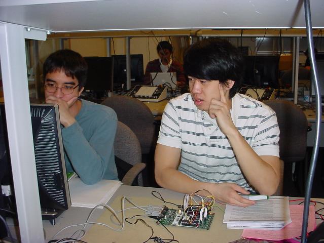
We would like to thank Skyler Schneider for taking some of the pictures used in this report as well as for providing the css file we modified.
- ATmega644 Datasheet
- AVR Instruction Set
- Documentation by Antti Lukatz with the Free AVR ICE Project
- Altera Jam STAPL freeware
- The Boundary Scan Handbook: Third Edition by Kenneth P. Parker (Google Book Preview)
- Prototype Board Layout
- Prototype Board Test Code by Bruce Land
- IEEE Code of Ethics