Digital Oscilloscope
ECE 4760 Final Project
Emily McAdams, egm23
Luke Diamente, lad97
Richard Wu, rsw35
Patent,
Copyright and Trademark Concerns
Microcontroller
Boards and Microcontrollers
Intellectual
Property Considerations
Ethical
and legal considerations
Introduction
The
goal of our project is to design a digital oscilloscope with 20 kHz bandwidth.
The scopes that we use in ECE 4760 lab cost over one thousand dollars. The
motivation of our project is to produce an affordable, easy to make
oscilloscope for students or other engineers who cannot afford to buy a
manufacturer’s oscilloscope. We are aiming for a range of up to 20 kHz and the
waveform is displayed on a 5 inch black and white television. Two
microcontrollers are used to store and print data onto the screen.
High Level Design
Oscilloscopes
are very versatile pieces of electronic test equipment that are used in a wide
variety of applications. For example, heart beat patterns can be displayed on a
specialized type of oscilloscope called an electrocardiogram. With all these
uses, we decided that it would be interesting to build our own 200 kHz digital
oscilloscope. This project presents difficulty in both hardware and software
design. Having a solid understanding of how this tool works will be essential
for our future as electrical engineers.
Background Math
This
project relies on sampling a waveform and then reconstructing it. The Shannon
sampling theorem, which states that samples must be taken at a rate greater
than twice the maximum frequency of the original signal (or at the Nyquist
rate), is used so that no aliasing occurs. Aliasing occurs when a signal
gets undersampled; a waveform of lower frequency will get reconstructed instead
of the correct higher frequency signal. A picture is shown below to illustrate
the idea:
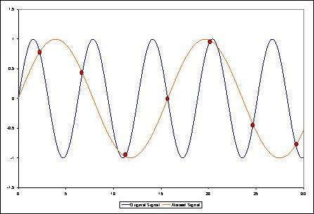
http://commons.wikimedia.org/wiki/Aliasing
The
undersampled waveform will have a frequency of:
falias
= fsample-rate – foriginal-signal
Therefore,
in this project, the sampling rate is always set higher than 40 kHz (the
oscilloscope functions correctly at a maximum frequency of 20 kHz). The A-to-D
converter is responsible for sampling and has a maximum sampling rate of 2
megasamples/sec.
Logical Structure
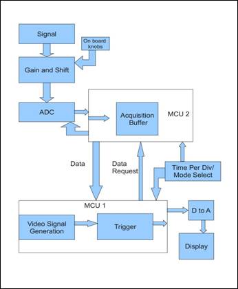
Figure 1: High level diagram
The
analog circuits on our board simply adjust the amplitude and level of the input
signal using standard op amp circuits. Depending on which time per div has been
selected, MCU2 acquires data at a specific number of samples per second as
determined by a timer. These samples are stored into the data buffer. Once it
is filled no new data can be stored until all of the points in the buffer have
been drawn. Also depending on the time per div selected, MCU1 will request a
certain number of data points per frame and draw these on the screen. For very
high frequencies it will draw many points per frame to appear more 'real time.'
Once MCU1 has drawn every point in the buffer MCU2 is free to start filling the
buffer up again. This cycle continues indefinitely until the time per div is
changed and the cycle then begins again.
Patent, Copyright and Trademark Concerns
The project uses some patented components as subcomponents.
However, there is no patent limitation on our final design as we are using the
devices as the manufacturer intended.
Hardware Design
Level Shifter and Amplifier
The
signal to be displayed is applied to the 100k resistor of the lower op amp. The
potentiometer can be adjusted to change the amplitude of the signal. The output
goes into a capacitor to remove any DC level and the resistive divider sets a
new DC level for the signal. The top op amp is designed to have an output from
0-5V. The two signals feed into a summing amplifier which adds the adjustable
DC signal to the fixed level, variable gain input signal. The output of this op
amp goes straight into the ADC.
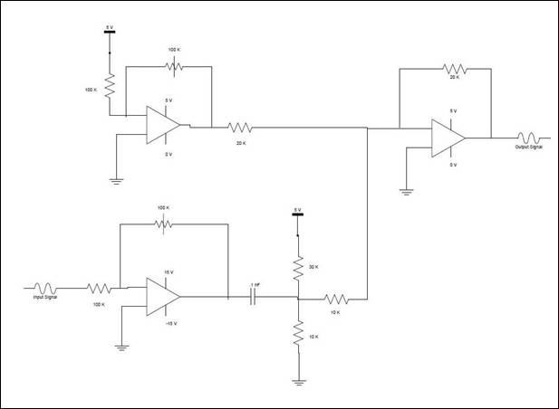
Figure 2: Schematic of proposed level shifter and
amplifier
Microcontroller Boards and Microcontrollers
In
order to achieve our bandwidth goals for the oscilloscope we had to use two
Atmel Mega644 microcontrollers. In order to use the microcontrollers without
the STK500s we had to build the custom PC boards designed by Bruce Land for
4760. In addition to the microcontrollers, the hardware we used on the board
was a DIP socket, six pin headers for the flash programmer, resistors and
capacitors, a voltage regulator, an LED, and a 16 MHz crystal. We did not need
serial communication for our project so we omitted the MAX233 and serial
connection port.

Figure 3: Populated prototype board designed by Bruce
Land
Digital to Analog Converter
The
video signal and sync signal were sent to the TV via port pins D.5 and D.6
respectively. A voltage of 0.3 V corresponded to a black pixel, while a
voltage of approximately 1.1 V corresponded to a white pixel. The sync
signal was a 0V signal. A sync pulse lasting 180 µs signaled the start of
a new frame, and a sync pulse lasting only 5 µs signaled the start of a new
line. We got the design for this DAC from ECE 4760 Lab 3.
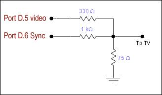
Figure 4: Schematic of Digital to Analog converter
Analog to Digital Converter
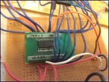
Figure 5: AD7825 in SOIC package
In
order to achieve the sampling rates needed to display the full range we want to
for this project we needed an external ADC. The Analog to Digital converter we
used is the AD7825 from Analog Devices. It is an 8-bit half-flash with 420 ns
of conversion time. Its maximum sample rate is 2 Megasamples per second. The
ADC works with signals in a voltage range from 0 V to 2.5 V when powered by a 5
V power supply. Since the ADC is the only external chip we are working with we
leave the Chip Select signal low to always have the chip selected and the Power
Down signal high to keep the ADC turned on. The ADC begins a conversion when
the CONVST signal goes from high to low. This signal may only stay low for a
maximum of 120 ns, otherwise the ADC will go into power down mode. When the
conversion has finished, the EOC signal from the ADC to the microcontroller
(which is hooked up to an external interrupt) goes low to trigger the
interrupt. Once the microcontroller sets the read bit low, the data from the
ADC is valid and the ISR can read data into the buffer. The read bit must be
sent back to high in order to reset the EOC signal. Another conversion cannot
start until at least 30 ns after the read has been set back to high.
Considering that the maximum clock rate for our MCU is 62.5 ns this is not a
limitation we had to deal with.
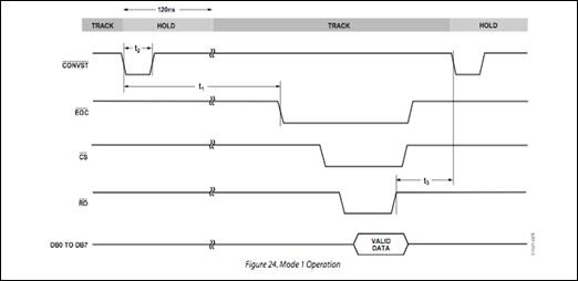
Figure 6: Timing diagram from AD7825 datasheet
Other Hardware
Other
hardware we used in our design included a Black and White Jenson TV with analog
input and five push buttons used to control the time per division of our
project.
Software Design
This project
included two microcontrollers in order to get the desired sampling rate and
successfully display the video. Therefore, we had to write a separate code file
for each microcontroller. One code file, named scope_calc.c, receives data from
the external ADC and transmits it to the other microcontroller. The other piece
of code, scope_video.c, handles receiving data from the other microcontroller,
setting up the data for display, and outputting the video signal to the black
and white TV. The fact that the MCU handling the video output is constrained to
a very specific timer and can have no other interrupts running is the reason we
need the second board.
Data Acquisition
This piece
of code is on the board responsible for communication with the ADC and sending
the data to the video board on request. This code has five main portions:
initialization, main(), INT0 ISR, INT1 ISR, and Timer0 compare match ISR. The
initialization first sets up all the ports that will be used in the program.
Port A is set up as input pins for Data from the ADC, Port B is also initialized as input for connections
to the push buttons. Port C is initialized to output and it is used for sending
data to the other board. Finally, 6 pins on Port D are set up to be output pins
used to configure the ADC and two are used as inputs for external interrupts.
|
|
Input/Output |
Assignment
|
Functionality |
|
D.0 |
Output |
ADC
Channel Select (A0) |
Always 0 |
|
D.1 |
Output |
ADC Channel
Select (A1) |
Always 0 |
|
D.2 |
Input |
ADC EOC |
INT0 ISR
triggered on falling edge |
|
D.3 |
Input |
Port C.0
on Video MCU |
INT1 ISR
triggered on falling edge |
|
D.4 |
Output |
ADC Power
Down |
Always 1 |
|
D.5 |
Output |
ADC Read |
Read Data
from ADC when low |
|
D.6 |
Output |
ADC Chip
Select |
Always 0 |
|
D.7 |
Output |
ADC
Convert Start |
1->0->1 to start a conversion |
Figure 7: Table with pin assignments for ADC communication
Initialization
also enables both external interrupts and sets them to trigger on the falling
edge of the signal. We chose falling edge because that is how the ADC we use
functions. (May adjust one to trigger on both edges – speed up our display time
– would fix our problem with displaying multiple points at once). Finally,
timer 0 is set up in the initialization. It is initially set to run at a low
sampling speed, for the lowest range of frequencies. The compare match
interrupt is enabled on this timer so it interrupts when the timer reaches the
value set in OCR0A.
The next
part of the scope_calc code is the main loop. The only thing in that happens in
this loop is that the push buttons are checked. The buttons are not debounced,
but for this particular application it does not matter. The buttons determine
what range of frequencies can be displayed on the screen. If a button is a
pushed the clock prescalar and the value of OCR0A are adjusted accordingly.
|
Push Button # |
Port
Connection |
TCCR0B |
OCR0A |
Frequency
Range |
|
1 |
B0 |
5 |
128 |
1 Hz – 10
Hz |
|
2 |
B1 |
5 |
25 |
10 Hz –
100 Hz |
|
3 |
B2 |
4 |
10 |
100 Hz –
800 Hz |
|
4 |
B3 |
2 |
35 |
800 Hz – 5
kHz |
|
5 |
B4 |
1 |
10 |
5 kHz – 20 kHz |
Figure 8: Table with prescalar and OCR0A assignments
External
interrupt INT0 is Pin D.2 on the microcontroller. The signal from the ADC which
indicates that a conversion has finished is attached to this pin. The ADC
signal, EOC, goes low when a conversion is finished, so the interrupt is set to
trigger on the falling edge of the signal. When the INT0 ISR executes it begins
by setting the value of D.5 (Read) to low to initiate a read. It then checks
the value of a variable named “lock.” If lock is low, then no data is stored in
the data buffer. Using “lock” controls whether or not data is read/written into
the data buffer. The ADC can convert data much faster than the video MCU can
read it out, so in order to control the data going to the video board, the
buffer must lock once it fills up until the video code reads out the rest of
the buffer. If lock is 0, then the data from the ADC is stored into the buffer
at 'inc.' 'Inc' is then incremented and it is checked whether or not inc
reaches the bounds of the buffer. If so, lock is set to 1 and inc is reset to
0. At the end of the ISR, read is set back to high. This interrupt will only
trigger once a conversion is ended and the rate of conversion starts is
determined by the clock prescalar and the value of OCR0A.
External
interrupt INT1 is Pin D.3 on the microcontroller. The signal from the video
board indicates that the video board is ready to read a byte of data stored in
the data buffer. When the interrupt is triggered the ISR puts a byte of data
onto PORT C to be read by the video board. It takes the byte of data in the
buffer at the increment 'video_inc.' It then increments the value and checks if
the value of 'video_inc' has exceeded the buffer size. If it has, then
video_inc and lock are both set back to zero.
The
final component of the scope_calc.c code is the ISR triggered by the Timer 0
compare match vector. The scalar of the timer and the value of OCR0A is changed
by the push buttons and determines the sampling rate. When this ISR triggers it
sets the value of D.7 (CONVST) to 0 and then back to 1 in order to trigger an
interrupt. Its important that D.7 stays 0 for less than 130 ns or else the
entire ADC will power down.
Video Generation
The purpose
of this board is to generate the oscilloscope's display onto the black and
white television. The signal generated must result in a frame being exactly
1/60 sec in order to conform to the NTSC standards. All of the code to generate
the actual signal is adapted from code provided by the ECE 4760 staff for Lab
3. The screen’s vertical number of lines
is 262, however only lines 30 – 230 are visible on the television screen. Every 1018 ticks of the clock, the timer’s
ISR would either perform synchronization tasks or actually print onto screen
using the byteblast() function. Byteblast() calls an assembly macro named
videobits to print the individual bytes to screen. Since the program is not outputting anything
to the screen during lines 231 to 262 and 0 to 29, this is where we do all of
the updates to the video screen. During this time the program checks the status
of the push buttons, requests and reads data from the calculation board, and
writes all of the information to be displayed to the screen in the next frame.
In the
initialization of the code, Port A is set up as input to read a byte of data
from the calculation board, Port B is initialized as inputs to read the push
buttons, Port C0 is set up as an output port and its signal is used to trigger
INT1 on the other microcontroller, and finally, Port D is set up as an output.
D.5 and D.6 are used to send the video signal to the TV. Also, the screen is
initialized, meaning that the borders and grid lines are drawn and
“OSCILLOSCOPE” is printed at the top of the screen.
Once the
screen line reaches 231, the code first checks the states of the push buttons.
If any of the buttons are pushed, the code changes the division state to the
appropriate time division and prints the value of the time division onto the
screen. The code then begins to read data from the calculation board. If the
boards are in a fast sampling state, the code reads 32 points of data at once.
If the code is in a slower sampling state, then the code only reads one point
of data. After the data has been acquired, the code then moves into a part
where it formats all the data to be displayed onto the screen.
The
next part of the video code formats the points to display onto the video
screen. If the scope is set in a fast sampling rate then all 32 points are
displayed onto the screen at once and if it is in one of the slower sampling
modes the code only prints one point in a frame. The code performs triggering
by keeping track of the peak of the signal. Once it reaches the end of the
screen, the code waits to redraw the signal until the peak point is reached.
The code is set to untrigger after 1000 frames. This is important because if
the level of the signal changes the code will need to set a new trigger.
Testing
Hardware Testing
The slew rate of a device is defined as
the maximum rate at which the voltage of an output can change given a particular
load capacitor.
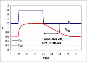
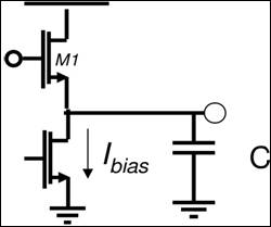
Figure 9: Slew rate illustration Figure 10: Slew rate in an amplifier
What we noticed in our hardware was
that the waveform between the output of our input op amp and the decoupling
capacitor was much distorted when the input was around 20kHz. We input a sine
wave and simply expected a larger sine wave back at the output. What we saw
instead was a triangle shaped wave with a funny kink at the tops and bottoms.
When we turned the frequency down or decreased the closed loop gain, the
phenomenon was still present but to a lesser extent. We realized that the
reason we were seeing this effect was that the output capacitance was a rather
large .1uF. This load is much more than the LM358 can drive at 20kHz with a 1V
swing.
Minimum slew rate to make 20kHz with 1V
swing : 2*(1/20kHz) = 100V/us. We were able to fix this problem by purchasing
the LM7171, a very high slew rate op amp.
Another problem we ran into was that
the method we used for biasing the decoupled input signal lead to a voltage
divider which attenuated the signal more than expected. In retrospect, this
divider was not necessary.
Software Testing
The majority of the software testing we
had to do for our project was testing the sampling rate and the interface with
the ADC converter. The first part of this testing was to figure out exactly how
fast we could signal the ADC to perform the conversion. We did this by setting
the prescalar of the clock and the OCR0A to different values and measuring the
interval between successive CONVST signals on the microcontroller. Since the
ADC can perform a conversion every 420 ns, we decided to test the CONVST signal
using the timer prescalar of 1 and setting OCR0A. According to calculations,
this means that the CONVST signal should be triggered every 625 ns. We found
that even running at this fast rate we were only signaling the ADC to start a
conversion every 7.2 us. We figured that this was due to the time required to
enter and exit the ISR.
|
Clock Scalar |
OCR0A |
Calculated
CONVST Interval |
Actual
CONVST Interval |
Frequency |
|
1 |
10 |
625 ns |
7.2 us |
136.6 kHz |
|
1 |
128 |
8 us |
8.08 us |
123.8 kHz |
|
1 |
255 |
15.94 us |
16.10 us |
62.5 kHz |
|
2 |
10 |
5 us |
7.6 us |
136.6 kHz |
|
2 |
128 |
64 us |
65 us |
15 kHz |
|
2 |
255 |
127.5 us |
128 us |
7.81 kHz |
|
3 |
10 |
40 us |
44 us |
22 kHz |
|
3 |
60 |
240 us |
260 us |
3.8 kHz |
Figure 11: Table with expected and
actual CONVST intervals
In testing the ADC, we also wanted to
make sure that our CONVST signal was not too fast on the ADC. Even though the
datasheet assured us that it only took 420 ns to complete a conversion and our
CONVST signaling interval was much greater than that time we wanted to make
sure that we were acquiring good data at fast sampling rates. We did this by
making sure EOC was back up to 1 before CONVST went low again.
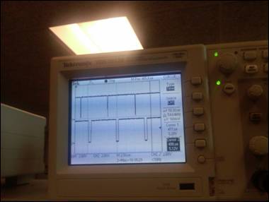
Figure 12: Signal on the top of the
screen is CONVST, the signal below is EOC
The final test we did with the ADC
included displaying the signal we were sampling on the oscilloscope and looking
at the RD signal so we could get some idea of how the signal was being sampled
and if the sampling rate was fast enough to get a good representation of the
signal.
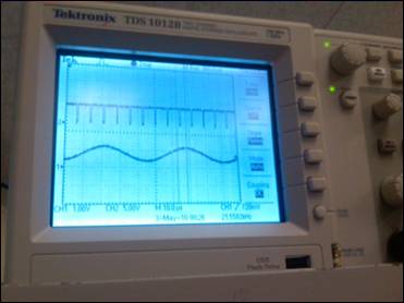
Figure 13: Sampling of a test signal
Results
Safety
During
construction of our circuit boards, we took many measures to ensure our safety
as well as the safety of others around us. We wore goggles when soldering and
made sure that the iron was at an appropriate temperature. After soldering, we
always turned off the iron.
Our
end product is very safe. Since we are not using any high voltage systems (the
highest voltage is 12 V used to power the microcontroller), our oscilloscope
does not present any opportunities for electric shock. We took care in our
wiring and tried to minimize the amount of exposed copper so that no accidental
shorts would happen. The only factor that presents a minimal safety concern is
the somewhat sharp edges on the circuit boards. However, if a user is attentive
and careful, the edges should not present any safety risk.
Usability
Our
project does have constraints on its usability. The frequency of a signal, as
well as what it looks like can be easily obtained from the oscilloscope.
However, our project has a limited input range from 0 V to 2.5 V. Any signal
that has an amplitude larger than this will damage the ADC. We could rectify this problem by creating a
better level shifter circuit to control the input signal. Furthermore, a user
currently cannot an exact amplitude reading from our current design. Finally,
we need to label the push buttons so that a user is aware of approximately what
time per division range he or she is selecting.
Accuracy
In
general, our oscilloscope is able to accurately represent a signal onto the
video screen. We measured the accuracy by inputting a signal with a known
frequency into the oscilloscope and estimated how many time divisions the
signal occupies on the screen noting that this method in itself creates error. We
then calculated the frequency of the signal based on how many time divisions
one cycle occupies and compare it back to the known frequency of the function.
We found that in general the higher frequencies resulted in a higher percentage
of error.
|
Our Measured Frequency |
Function Generator Frequency |
Percent Error |
|
10.5 Hz |
10 Hz |
4.80% |
|
95.7 Hz |
100 Hz |
4.50% |
|
1.66 kHz |
1.5 kHz |
9.6% |
|
4.76 kHz |
5 kHz |
5.04% |
|
22.4 kHz |
20 kHz |
10.70% |
Figure 14: Table showing accuracy of
oscilloscope measurements
Conclusion
Our
project met our expectation as a functional oscilloscope. However, we did not
meet our expectations in the features that we were going to add to the
oscilloscope. We are able to display good resolution waveforms between
frequencies ranging from 1 Hz to 2 kHz. By pushing one of five push buttons,
the oscilloscope will change its time per division setting. This functionality
worked flawlessly as the user can either analyze a small section of a waveform
or increase the time span to analyze a longer portion of a waveform.
Unfortunately, our level shifter and attenuator circuit did not work too well.
The attenuator attenuated our signal too much, while the level shifter only
shifted the DC point by about 100 mV. Furthermore, we did not have enough time
to implement a spectrum analyzer, as debugging took much more time than
expected.
Our
greatest challenge was to figure out how the data was going to be transferred
between the two microcontrollers. We tried various different approaches when working on this. We started by
using a handshake protocol between the two boards, but found that it was slow
and unreliable. We got the idea of using an external interrupt on the
acquisition board from the method of communication with the ADC. We found that
it was the quickest way and did not require two handshake signals, just the one
external interrupt signal.
Our project required a tremendous amount of wiring and we definitely could have
organized this much better. Optimizing where each circuit would go and
shortening the lengths of the wires would have made ourproject more neat and
presentable. To improve usability, we could have labeled the push buttons so
that the user would know which button corresponded to which time per division.
Also, we could have implemented some cursors to display on the TV screen. This
would make measuring the time per divisions much more accurate compared to just
eye-balling them on the screen.
The
analog front end could have been implemented much better if we had more time.
The original plan was to use a bipolar supply but this seemed to cause excess
heat in the op amps. This would have increased our input swing and give us the
ability to shift the signal down as well as up. Also, the biasing resistors
could have been increased to reduce attenuation without having to have large
gain into the
capacitive load.
Intellectual Property Considerations
Since
an oscilloscope was built as a final project in a previous year for ECE 4760,
we looked at how the other group had done their project (http://www.nbb.cornell.edu/neurobio/land/PROJECTS/VideoScope/). We noticed that they used a black and white TV to display
the waveform, so we decided to do the same. We also looked at Yi Yao's website
(http://yyao.ca/projects/oscilloscope/) for ideas. Our logical structure is
partly based on Yi Yao's block diagram. We did not use any of the code that Yi
Yao provided. Furthermore, we looked at the instructions for the oscilloscope
lab done in previous years for ECE 4760
(http://instruct1.cit.cornell.edu/courses/ee476/labs/s2007/lab4.html). However,
we did not get any ideas from this; for the most part, our design was
completely independent of what was done before. We do not believe that there
are patent opportunities for our project since oscilloscopes are widely
available.
Ethical and legal considerations
During the
design of this project, we strived to follow the IEEE Code of Ethics. Our
project does not present any safety or health concerns to the public. While
constructing the circuits, we were very careful with the soldering irons so
that it did not burn us nor anyone around us. Our results are stated honestly
and truthfully; we did not manipulate any of our data. While working on the
project, we tried to maintain a safe and supportive environment. We treated our
peers with respect and took everybody's suggestions and criticisms seriously.
We also helped other groups by providing items that they needed. Our
oscilloscope is meant to provide students with a better understanding of how
electronics work. It is an incredibly useful tool for debugging circuits as
well as measuring voltages. Through our project, we hope that there can be an
improved understanding of technology. For us, this is definately true, as we
have learned so much after completing this assignment. We do not intend to sell
our product in the market so there are no legal considerations. If we did, then
product safety must be considered.
Appendices
A. Datasheets
LM 7171 Op
Amp: http://www.national.com/ds/LM/LM7171.pdf
AD 7825 Analog
to Digital Converter: http://www.analog.com/static/imported-files/data_sheets/AD7822_7825_7829.pdf
Atmel
MEGA644: http://instruct1.cit.cornell.edu/courses/ee476/AtmelStuff/mega644full.pdf
B. Budget
|
Item |
Number |
Supplier |
Cost |
|
Custom PC Board |
2 |
4760 Lab |
$
8.00 |
|
Mega644 |
2 |
4760 Lab |
$
16.00 |
|
B/W TV |
1 |
4760 Lab |
$
1.00 |
|
6 Inch Solder Board |
3 |
4760 Lab |
$
7.50 |
|
2 Inch Solder board |
2 |
4760 Lab |
$
2.00 |
|
Power Supply |
2 |
4760 Lab |
$
10.00 |
|
DIP socket |
2 |
4760 Lab |
$
1.00 |
|
Pin Headers |
40 |
4760 Lab |
$
2.00 |
|
AD7825 |
1 |
Analog Devices |
$
- |
|
1 Pin Jumper Cables |
3 |
4760 Lab |
$
4.00 |
|
Alligator Clips |
3 |
4760 Lab |
$
- |
|
SOIC Carrier Board |
1 |
4760 Lab |
$
1.00 |
|
Op Amps (Not LM358) |
2 |
Digikey - National
Semiconductor |
$
5.66 |
|
Resistors/Capacitors/Push
Buttons |
Many |
4760 Lab |
$
- |
|
|
Total Cost |
|
$ 58.16 |
Figure 15: Table with project budget
C. Commented Code Listing
D. Schematic
E. Division of Labor
Most of the
work on this project was done by all three group members working together. All
three members were involved in the physical construction of the project as well
as the testing and debugging. Luke and Richard did focus more on the analog
circuit design of the level shifter and amplifiers while Emily worked more on the
code, particularly on scope_calc.c and interfacing with the ADC.
F. Special Thanks
We
would like to thank Bruce Land, the course instructor, for providing the lab
space and other materials we needed for the project along with much guidance.
We would also like to thank TAs Yuchen Zhang and Jeff Melville for helping us
in lab and helping us out as we got stuck along the way. Also, Analog Devices
for providing samples of the AD7825 we used in our project.