This project was completed by Alexander Schlichting and Michael Shafer, both in the Sibley School of Mechanical Engineering Ph.D. program. They work in the Laboratory for Intelligent Machine Systems directed by Prof. Ephrahim Garcia. The motivation for this project was provided by the NSF Lab-on-a-Bird collaborative grant under the guidance of P.I.'s Prof. Erickson, Prof. Ephrahim Garcia, and Prof. David Winkler.
Introduction
The tags used to monitor wildlife can either be passive or active. Passive tags simply identify an individual, whereas active tags may send out a radio beacon or even collect data. These active tags, more commonly referred to as “bio-loggers”, are typically battery powered, and thus have limited life. This is especially true for birds given their limits on payload capacity. We are interested in extending the life of these tags by harvesting energy from the bird or the ambient environment, and using it to recharge the battery. This stored energy could then be used to collect environmental data, location data, possibly take in-vivo physiological measurements for the bird, and transmit data. For this project, we are interested in developing the circuitry and the microcontroller (MCU) programs necessary to indefinitely extend the lifetime of a battery powered MCU system.
High Level Design
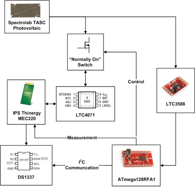
To develop the bio-logger, various subsystems need to be developed and integrated. The main subsystems are the microcontroller, power management system, and sensor suite. For this project we are focusing on developing the microcontroller and power management systems as seen in Figure 1. We will use this system as a basis for future added functionality that will include a sensor suite and piezoelectric harvester.
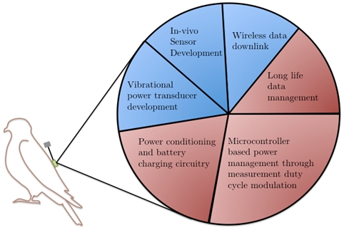
We have chosen to focus our efforts on developing the microcontroller code and electronics necessary for a system to monitor the state of its battery and modulate the instrument measurement duty cycles such that the system does not use more power than what is being harvested from the environment. To do this, we focused on three areas: power conditioning and battery charging, the microcontroller code for managing microcontroller operation based on the battery state, and the microcontroller code necessary for managing large data sets. For each of these sub-tasks, we asked specific questions at the outset of the project, with the intention of answering them at the conclusion. These were:
How do you charge a battery, or array of batteries from multiple sources including high voltage AC (piezoelectrics) and low voltage DC (solar)? What voltage conditioning is necessary? What charging electronics are necessary? How can you regulate the battery voltage to a level that is acceptable to all circuit components in use?
Can a microcontroller monitor the state of its own battery and modulate its own operation based on the state of charge? What is the lowest amount of power that the MCU can draw? Can the system keep track of the date and time when the MCU is in a low power mode?
How can the system store the logged data for extended periods of time when the system loses power? How can the memory be used to help the system understand its own state? How should data points be logged such that data is not overwritten?
With these questions in mind, we were able to begin development of each of these sub-components. The power conditioning and battery charging circuitry was developed in parallel with the microcontroller and data designs. This allowed for independent debugging of the systems prior to system integration. Once both systems were functional, system level testing commenced.
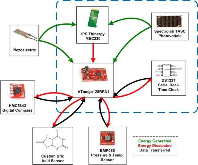
A high-level view of the components used in this project, and those expected to be incorporated at a later date as part of research, can be seen in Figure 2. In this figure, we show the major components of the power and data management system. Our project uses an Atmega128RFA1 microcontroller as the system hub. This is a more capable MCU than the Atmega644 used in class. It uses less power, has a wider array of peripherals, and most importantly, has an integrated 2.4 GHz radio that we can use in the future for wireless downlinking of the data. We use Inifite Power Solutions Thinergy thin film batteries as an energy storage source and Spectrolab, 30% efficient GaAs, TASC solar cells. Finally, one of the most important components in the system is the Maxim DS1337 low-power external real-time clock. Because the bio-logger is essentially a small-scale data acquisition system, it is critical that the time of each measurement be known. And because these systems are expected to operate over the course of years, the system needs a clock source that is continuous from the date of deployment. We have chosen this clock because it is extremely low power, and as such, allows the system to keep track of time over the course of years, assuming the batteries are occasionally charged. Even without charging of the batteries, one fully charged Thinergy MEC201 battery could power the clock for approximately 25 days. Because this clock was designed to use such low power, it does almost no conditioning of the time registers. We the time read over the I2C bus must be converted using software to a typical Gregorian date. This is one of the major tradeoffs in this system between hardware and software. We were required to make more complicated code to deal with simple, but highly efficient hardware. Another tradeoff between software and hardware for our system, although in the other direction, is using a battery charging/discharging control I.C. to protect our batteries. While the same functionality could be achieved using battery voltage measurements with the MCU, the long sleep cycles desired for this system would leave the battery completely unprotected during this time if it were to be done using software.
While neither specific patents, nor standards could be found pertaining to self-charging bio-loggers, there are companies that produce battery powered tags. One such company is Wildlife Computers. They produce a variety of wildlife tags, all of which are powered from large batteries. Four of their tags are shown in Table 1 for reference. These tags all have lifetimes that extend out close to, or more than a year, but their mass is approximately 1-2 orders of magnitude too high for use on most bird species. Our system is designed to be extremely light-weight, and will have lifetimes that far exceed those specified for these systems.
 |
 |
 |
 |
|
| Name | SPOT Tag | SPLASH Tag | SPLASH Tag | SPOT Tag |
|---|---|---|---|---|
| Mass (g) | 110 | 114 | 200 | 54 |
| Lifetime (days) | 840 | 250 | 500 | 260 |
Hardware Design
Power System Design
To provide power to the ATmega128RFA1 MCU, two different sources are used: solar and battery power. The configuration of the power circuit used for this system was taken from the combination of example circuits shown for the use of the LTC4071 battery charger I.C. (will be discussed below) in its data sheet, which can be found linked at the end of this document. The Spectrolab's TASC solar panels have the ability to directly power the MCU and recharge the Infinite Power Solutions MEC220 batteries. At their maximum power output, each of the panels can produce 2.19 V at 28 mA. The MEC220's have a voltage rating of 4.1 V, however, and two TASC solar panels must be connected in series to achieve the necessary voltage level for one battery. The power from both of these sources is conditioned using the LTC3588 Piezoelectric Energy Harvesting Power Supply. While we are not performing piezoelectric energy harvesting with this system, future systems could require that functionality and the LTC3588 can accomodate DC energy sources as well, making it very versatile and applicable to our system. To produce the 3.3 V supply voltage for powering the MCU, the LTC3588 requires at least 5.05 V to initiate its output. Therefore, a stack of two of the MEC220's in series is required to provide the necessary voltages for the LTC3588. Also, now that the system requires two MEC220's in series, creating a total battery stack maximum voltage of 8.2 V, it also requires 4 of the TASC solar panels in series for the panels to be able to recharge the batteries.
Each of the MEC220 batteries is protected from over-charging/discharging using an LTC4071 Li-Ion/Polymer Shunt Battery Charger System with Low Battery Disconnect. This chip rails the maximum voltage seen by the battery to the 4.1 V specified by the MEC220 by shunting energy, protecting it from over-charging. The chip also completely disconnects the battery if its voltage goes below 2.7 V to prevent it from being over-discharged. As Figure 4 illustrates the results of the low battery disconnect behavior of the LTC4071. In this plot, four separate batteries are fully discharged, each using a 10 kΩ load. The two red curves show the dicharging of the MEC220-3S's (their standard batteries) and the two blue curves the MEC220-4P's (the performance versions). First, we can see the difference in the reported capacities of the two different versions of the cells as the MEC220-3S is listed at 300 μAh and the MEC220-4P at 400 μAh. Next, it is clear that any two cells, even from the same line, can not be expected to have exactly the same capacity. This difference is more apparant with the standard cells than with the performance cells.
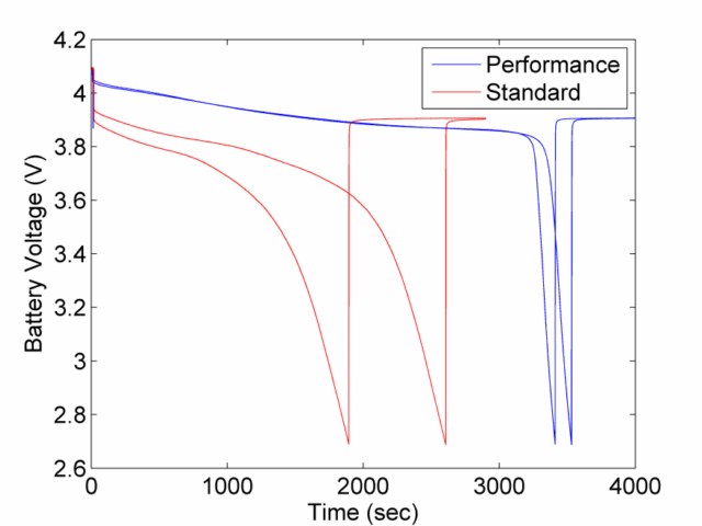
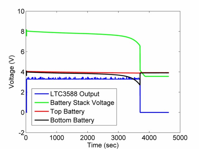
Figure 5 shows the results of a discharge test using a two-cell battery stack (MEC220-3S) with the LTC3588. The blue curve shows the 3.3 V output of the LTC3588, which cuts out once the battery stack voltage drops to below the worst-case 3.9 V specified to continue the 3.3V output. The effects of the different battery capacities can be seen by noticing that this drop occurs when the battery stack voltage is still above 6.0 V. Theoretically, if each of the LTC4071's disconnects the battery when it reaches 2.7 V, then we should see operation down until 5.4 V. However, if one of the batteries reaches 2.7 V significantly before the other, it is locked out and we experience a 2.7 V drop in voltage for the entire battery stack. If the other battery's voltage is below 3.9 V at this time, then the LTC3588 can no longer sustain its output. This significantly reduces the range of expected voltages for the battery stack during safe periods of operation as well as the overall usable energy the batteries can store.
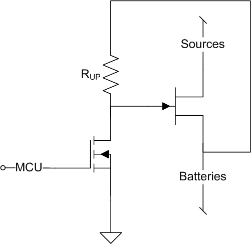
The remaining functionality of the system hardware involving the power system revolves around the MCU communicating with and controlling the battery stack. For lithium-ion/polymer batteries, the current state of charge (S.O.C.) can be approximated quite accurately using the open-circuit (O.C.) voltage of the cell. To measure the actual O.C. voltage of the cell, not only must it be disconnected from the load, but the cell must be allowed to reach a steady-state. After the load is initially removed, the voltage rises by an amount and at a rate dependent on the load characteristics as well as the battery chemistry and capacity. To this end, a normally-on switch is added at the top of the battery stack to disconnect it from the solar cells and the LTC3588. Due to the significant difference between the 3.3 V logic-high output available from the MCU and the voltage expected from both the sources and batteries, a level-shifter topology is adapated. Also, as we do not want the batteries to be permentantly locked out if the MCU loses power, the switch has to be "Normally On". This is accomplished by using an N-channel MOSFET and an N-channel JFET, as shown in Figure 6.
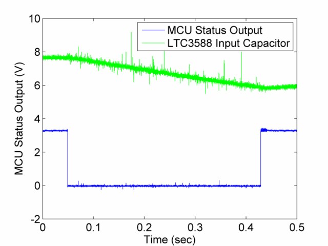
The LTC3588 requires a capacitor to be placed between its VIN pin and ground. When the battery stack is disconnected to measure the O.C. voltage of the cells and estimate the S.O.C. of the batteries, the MCU power is being provided from this capacitor. So, this capacitor size depends on the length of time where the battery is completely disconnected for each one of these measurements. However, as Figure 7 shows, this capacitor is drained whenever the MCU is in its active state, not just when the battery stack is disconnected. Therefore, the input capacitor has to be sized such that its voltage does not drop below the worst-case 3.9 V required for the LTC3588 to continue its 3.3 V output during any of the MCU operations. This behavior can be understood by noting the differences in discharge characteristics of a battery as compared to a capacitor. Batteries can provide more constant-voltage, low-power loads for long periods of time. This is due to the chemistry of the cells themselves. Capacitors are able to provide power at significantly higher frequencies and can therefore deal with the sudden shifts in power draw caused by shifting in and out of sleep cycles. Therefore, even though the batteries possess the energy to fully power the MCU during its active cycle, the input capacitor is drained first as it is the more readily available source. As a result, to provide power for the 380 ms the MCU is active during each of its operation, a 1 mF capacitor is required.
Timing System Design
The MCU uses I2C communication with the DS1337 Serial Real-Time Clock to govern its sleep cycles. This is necessary as using the integrated methods for waking up from sleep only grants us a maximum of approximately 8 seconds for each sleep period. As our end goal for this project will entail having the MCU sleep for multiple hours at a time, longer timescales are necessary. The DS1337 provides us with two alarms which are programmable to trigger after periods on timescales ranging from 100 years to seconds. The output trigger from the DS1337 is used for a hardware interrupt to wake the MCU. One issue is that if the DS1337 loses power, then it stops keeping track of time. This situation must be avoided otherwise the validity of the time-stamps for the data points will always be suspect. The timekeeping operations of the DS1337 can continue all the way down to 1.3 V, which provides some significant flexibility on powering the chip. Due to its low maximum timekeeping current draw of 600 nA, it can be directly connected to the lower battery in the stack without significant worry of it overdischarging the battery. This is futhered by the fact that the LTC4071 cuts out the battery from the rest of the system at 2.7 V, while the MEC220 datasheet has a minimum safe battery operation voltage of 2.1 V, providing a decent window of safe operation of the clock during total system shutdown before the battery is damaged.
Overall System Design
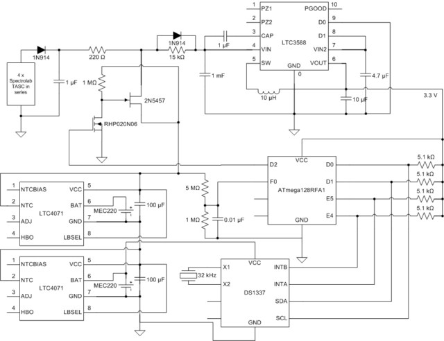
Figure 8 shows the end circuit schematic of all of the hardware of the system. All of the different aforementioned components and their necessary additional passive components are shown. There are a couple of further items of note. First, for the resistive voltage divider used to drop down the battery stack voltage to levels readable by the MCU, a small capacitor must be placed in parallel with the bottom resistor. Due to the significant impedances used for the voltage divider to minimize energy dissipation, this is required to create a fast response time for the ADC's voltage measurement. Second, there is a high-frequency switching diode (1N914) and a resistive load between the input of the LTC3588 and the top of the battery stack and the solar cells. For the case when there is a piezoelectric source input to the PZ1 and PZ2 pins of the LTC3588, the resistive load is necesary to prevent excessive current from the piezoelectric charging the batteries. This is particularly an issue due to the high voltage levels possible from piezoelectric sources and the 50 mA maximum shunting current for the LTC4071. The 1N914 allows for unimpeded current flow from the battery stack and solar cells to the LTC3588, minus the semiconductor voltage drop. While for this system a piezoelectric energy source is not being used, these components were included such that one can be incorporated with minimal effort.
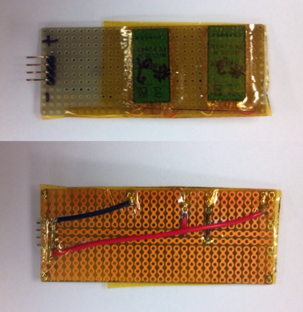
Figures 9 - 12 show the finished prototype components. Figure 9 shows the top and bottom of the power conditioning circuitry of the system. Specifically, on this board is the LTC3588 breakout board from Sparkfun Electronics and the two LTC4071 chips. The solar cells connect to the two-pronged 90 degree header at the top of the picture. The battery pack with the two batteries connects to the four-pronged 90 degree header at the bottom left of the picture. The five-pronged 90 degree header at the bottom right connects to the MCU.
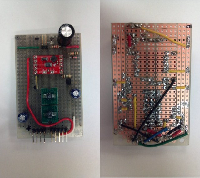
Figure 10 shows one of the battery packs used for the system. As the cells are quite fragile and intended for mounting on a PCB, this setup was developed to protect the cells from damage during testing. Each of the cells is encased in Kapton and adhered to the top of the board. The wiring on the back of the board from the battery terminals to the plug is also encased in Kapton.
The four TASC solar cells also need to be protected. The protective casing, including a glass slide window, is shown in Figure 11.
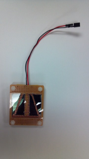
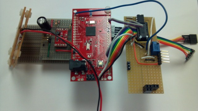
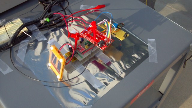
Figure 12(a) shows the overall system with the ATmega128RFA1 Sparkfun development board in the foreground in red. The protoboard directly to the right of it has the DS1337 clock on it. These are mounted above the power circuitry using headers. The entire setup was placed on a cart with an oscilloscope to allow for real-time monitoring of outdoor testing (Figure 12(b)). The probes attached to the system allow us to monitor the MCU's operation state using a pin which outputs logic high when asleep and logic low when active and the battery stack voltage level.
 |
 |
| (a) | (b) |
System Component Power Characteristics
As this is a battery and solar powered system, the power consumption characteristics of the components is a very important design factor. First, Table 2 shows the basic power consumption characteristics we should expect for the ATmega128RFA1 MCU for the two different modes which are used for this system.
| Operating Mode | Supply Current (μA) |
|---|---|
| Active, 16MHz External Crystal | 4500 |
| Deep Sleep Mode | 0.25 |
As is evident, the active mode of the MCU is the most significant power draw for the system. The battery charger/discharger circuit consumes very little power when it is not actively shunting any energy (Table 3). One key aspect is that the LTC4071 draws only 550 nA from the battery when the low battery disconnect logic has been enabled and the battery is isolated from everything but its LTC4071 chip. This is a very minimal amount and should help minimize the risk of damaging the batteries during periods when the battery is isloated from the system load by the chip.
| Type | Supply Current (nA) |
|---|---|
| VCC operating current | 550-1200 |
| Battery disconnect leakage current | .01-25 |
The DS1337 clock consumes minimal power as well. The clock is connected directly to one of the batteries to minimize the chances of a complete loss of power and by extension the loss of accuracy of the clock's timekeeping ability. Therefore its power consumption must be small enough such that when there is a complete system shutdown, and there is no source of power, the chances of over-discharging the battery are minimal. Table 4 shows that this is the case. Also, for the Timekeeping mode supply current, our system does not take advantage of the oscillator, so the actual power consumption is in fact less than the reported number and was measured at 0.6 μ.
| Mode | Supply Current (μA) |
|---|---|
| Full Operation VCC = 1.8 - 5.5 V | |
| Active (I2C communication) | 150 |
| Standby (Timekeeping) | 1.5 |
| Timekeeping Operation VCC = 1.3 - 1.8 V | |
| Timekeeping (oscillator enabled) | 0.425-0.6 |
| Data Retention (oscillator disabled) | 0.1 |
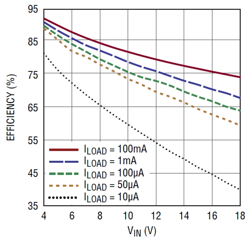
The final integrated circuit component with the potential of drawing significant amounts of power from the system is the LTC3588 chip. Figure 13 shows the efficiency power curves of the integrated voltage regulator for a 3.3 V output and 10 μH inductor. For an approximate input voltage of 8 V for our system, we'll see an efficiency range of 65 to 80%.
Program Design
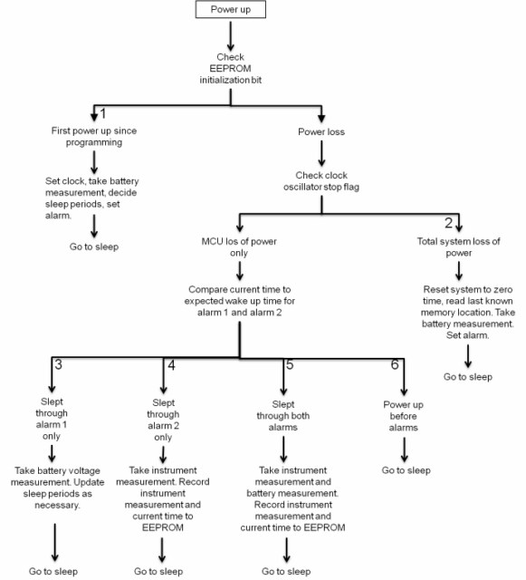
The lab on a bird power and data management code uses knowledge of the state of the system to dictate the times between measurements. To do this, the MCU must interact with the DS1337 external real-time clock, the EEPROM memory, and the raw battery voltage. The general operation of the program is as follows: 1) The system wakes up, either through an external interrupt of from the external clock or from a power up of the system. 2) The system then checks various settings to determine the state in which it has awoken (initial power up, secondary power up, alarm 1, etc.). 3) Once the startup state is known the alarms are reset as necessary given the current state. 4)Depending on the startup state, the system may then take an instrument measurement and record it to EEPROM. 5)In all cases, the system then goes back to sleep.
The first operation that must be completed when power is supplied is to determine the state of the system. There are six potential states at power up.
- Initial power up after programming
- Total system loss of power
- MCU loss of power, clock okay, slept through alarm 1.
- MCU loss of power, clock okay, slept through alarm 2.
- MCU loss of power, clock okay, slept through both alarms.
- CPU loss of power, clock okay, did not sleep through any alarm.
This power up state should happen only once for a given deployment of the system. When the system is programmed, 0x00 is written to EEPROM byte zero. After the first power up after programming, the MCU writes 0x01 to this memory location. This bit is used by the MCU to determine if a clock reset is necessary. During the initial power up after programming, the system will see 0x00 and set the clock. Subsequent power up events will see 0x01 in this memory location, and will not reset the clock. The only exception to this is if the system starts up in case 2.
For this case, the entire system lost power. This includes the MCU and the external clock. With the loss of power to the clock, the system will be unable to know what time it is and will reset the clock to zero time. By resetting the clock, the post processing code is able to see clock resets and convey that information to the user. Subsequent date and time measurements will be uncertain.
In this case, the CPU has lost power but the clock maintains power. Upon wakeup, the system will compare the current clock time to that of the expected wakeup time to determine if it has slept through alarm 1. Such a long duration of power loss to the CPU could occur in the case when the input voltage to the buck converter of the LTC3588 drops below the under voltage lockout of 3.67 V. If this happens, the 3.3 V output of the buck converter will not be restored until a charge source is applied to the batteries. This is due to the fact that the LTC4071 will lockout the battery if Vin drops below 2.7 V. It will not allow for output until a charge source is applied.
This is the same as case 3 except the system has slept through alarm 2.
This is the same as case 3 except the system has slept through both alarms.
In this case, the MCU has lost power, but it is restored before either of the alarms were set to go off. In this case, the system simply goes back to sleep.
The flow chart shown in Figure 14 shows the logic used to determine the state of the machine after being powered up. All states terminate in the system being put back to sleep and waiting for the external interrupt of the clock to wake the system. These states are used to get the system back online if the power is lost. Such events should be rare, and the more typical wakeup event results from an external interrupt awaking the MCU.
During normal operation, the system can be awoken by either of the two alarms on the DS1337. These pass to external interrupts four and five on the MCU. We have chosen alarm 1 to be used to dictate when the battery should be measured and monitored, and alarm 2 for use as an instrument measurement alarm. While we have developed our code to be able to respond to two types of alarms, and it is capable of setting both alarms, we have elected to not incorporate a sensor on the system at this time and will use battery voltage measurements to simulate sensor data.
When the system is awoken by alarm 1 it initially takes a battery voltage measurement. To do this, the program disconnects the batteries from the LTC3588 by setting PORTD.2 high. This is done so that a open circuit voltage can be measured. The battery voltage is then measured using the measure_volt() function. A detailed description of the functions used in this code can be found in the Function Descriptions sub-section. Upon taking this battery measurement, the system then passes this information to the period() function to determine how much time should elapse before the next alarm. The period() function provides main() with a delta time between the current time and the next wakeup event. Main() then uses the add_time() function to add this delta time to that of the current clock value. The resulting future time is passed to the set_alrm*() function, which sets the appropriate alarm. Main() then records the expected wake-up time for alarm 1 in memory locations 3-10 and calls the sleep_point() function. The sleep_point() function contains the code necessary to put the system into a deep sleep with minimal power usage. It calls up sub functions that shut down peripherals and then puts the system to sleep. Upon waking, the external interrupt service routine first disables external interrupts to prevent the low line from retriggering the interrupt. The alarm flag on the clock is then reset to bring the interrupt pin back high. The system then returns to the sleep_point() function from the ISR. The function restarts the peripherals and then returns operation to main(). The sleep_point() function occurs at the end of the infinite while loop such that upon waking, the system starts again at the beginning of the while loop.
EEPROM Memory Mapping
Below is the memory mapping for the EEPROM data stored on the microcontroller. The memory space is broken up into two main sections: header and data. The header information contains data that the MCU needs to keep track of the state of the system as well as the current memory location, so as not to overwrite the most recent data. This header data is held in bytes 0 through 27. The current memory location contains the next memory address where data can be written. It is not the last address to which data was written. The remainder of the EEPROM memory is used for data storage. When Julian dates are written to EEPROM, they are written in two blocks. The first 4 byte block holds the whole date Julian date and the second 4 bye block holds the fraction of the day. For data recordings, after the Julian date block is a 4 byte block containing the voltage measurement. In total, each data recording requires 12 bytes for the date and measurement.
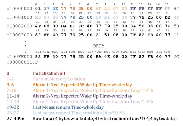
The memory mapping in Figure 15 is in an Intel Hex format. The first four bytes of each line contain information as to the type of information stored in that line and the memory address number. The subsequent 16 bytes are the data and the last byte is a check sum byte. More information on this format and the calculations necessary for the checksum byte can be found in the Intel HEX standard linked in the Appendix.
Function Descriptions
void init_mcu();
This function initializes the pins on the MCU for triggering of the battery disconnect. It also calls other initialization functions such as i2c_init() and init_uart(). This function sets the sleep mode for the system as ‘power down mode’ and turns off the alarm outputs on the clock incase they hadn’t been reset at the last power up event.
void init_ei (int ei, char type);
Initializes the external interrupt pin specified by the ‘ei’ variable. The variable ‘ei’ can range from 0-7 for each of the external interrupts, the ‘type’ variable dictates the type of interrupt to be used. Type ‘l’ is for low level interrupt. Type ‘a’ is for any voltage edge interrupt. Type ‘f’ is for voltage falling edge interrupt. Type ‘r’ is for voltage falling edge interrupt. Note that per the Atmega128RFA1 specifications, if the MCU is to be awoken using one of the external interrupts, the interrupt must be set to the low level.
void init_lcd(void);
This function initialized the LCD for the Atmega128RFA1. It is not used in the final version of the code.
void init_uart(void);
This function initialized the UART system on the Atmega128RFA1. This was used for debugging and demo purposes only and is not part f the final version of the code.
void set_clck(void);
This function sets the DS1337 external real time clock to January 1, 2012 at 00:00:00.
void set_alm1(uint8_t time[4], char repeat);
This function sets alarm1 on the DS1337 external real time clock. The caller must pass an array of times [date,hour,minute,second] for when the alarm should go off. The ‘repeat’ variable can be set to ‘s’, ‘m’, ‘h’, ‘D’, ‘d’ for the alarm to repeat when the second, minutes, hours, date, or day match, respectively.
void set_alm2(uint8_t time[4], char repeat);
This function sets alarm1 on the DS1337 external real time clock. The caller must pass an array of times [date,hour,minute,second] for when the alarm should go off. The ‘repeat’ variable can be set to ‘m’, ‘h’, ‘D’, ‘d’ for the alarm to repeat when the second, minutes, hours, date, or day match, respectively.
int get_time(char unit);
The get_time function queries the DS1337 real time clock as to the current time in ‘units’. The variable ‘unit’ can be set to ‘s’, ‘m’, ‘h’, ‘d’, ‘D’. ‘M’, or ‘Y’. For example, get_time(‘D’) would return 17 if the current date was March 17, 2012.
int cnvrt_to_clck(int number, char unit);
This function converts any number to the 8 bit format used by the external real time clock. The ‘unit’ variable can be set to ‘s’, ‘m’, ‘h’, ‘d’, ‘D’. ‘M’, or ‘Y’.
int cnvrt_from_clck(int number, char unit);
This function converts any 8 bit number read from the DS1337 external real time clock to a normal integer. The ‘unit’ variable can be set to ‘s’, ‘m’, ‘h’, ‘d’, ‘D’. ‘M’, or ‘Y’.
void write_bit(int logical, int bit, int reg_addr,int dev_addr);
This function writes a single bit to any device across the I2C bus. The caller must provide the address of the device on the I2C bus, the address of the register on which the bit in question exists, the bit number within that register, and the desired logic to be written to that bit (0 or 1). This function is useful in setting up configuration bits on I2C devices.
int read_bit( int bit, int reg_addr,int dev_addr);
This function reads any bit on an I2C device. It is useful for helping to determine the current settings of an I2C device. The caller must provide the address of the device on the I2C bus, the address of the register on which the bit in question exists, and the bit number within that register.
void cnvt_from_jd(long int JD_abs,double frac_day, int *p_time);
This function converts a Julian date number to a Gregorian date using an algorithm based on that presented on the US Naval Observatory website. This algorithm is based on the following publication: Fliegel, H. & can Flandern, T.C. 198, Communications of the ACM, 11, 657. This function accepts the Julian date as two variables. The first is the whole day portion of the date (‘JD_abs’). The second variable (‘frac_day’) is the fraction of the day. The resulting Gregorian date is saved to the array starting at the pointer location *p_time. This should be a integer array of size seven. Note that this function currently is not able to resolve fractions of a second and as a result may an error of 1 second.
void cnvt_to_jd(int time[7], long *p_JD, double *p_JD_frac);
This function converts a Gregorian date to a Julian date number using an algorithm based on that presented on the US Naval Observatory website. This algorithm is based on the following publication: Fliegel, H. & can Flandern, T.C. 198, Communications of the ACM, 11, 657. The function accepts an input array of size seven containing the Gregorian date ([year, month, date, day, hour, minute, second]). The pointers p_JD and p_JD_frac, should point to the desired location of the resulting Julian date and fraction of a day, respectively. Note that this function currently is not able to resolve fractions of a second and as a result may be off by 1 second.
void add_time(int time[7], int delta[7], int *p_time_result);
The add_time function allows for simple increments in the current time. It is useful when setting alarms. The caller provides the Gregorian date array (‘time[7]’) and the amount time to be added (‘delta[7]’). The function converts these to Julian dates, adds the time and then converts back to a Gregorian date. The resulting Gregorian date array is saved to the location point to by ‘p_time_result’.
double measure_volt(uint8_t channel);
This function measures the voltage applied to any ADC channel as specified by the ‘channel’ variable. It initializes the ADC system takes a measurement and then returns the resulting measurement as a floating-point number. Note that this function uses the global ‘scale’ variable to scale the ADC result to a floating-point number.
void PRR_sleep(void);
The Power Reduction Register sleep function is to be used immediately prior to sleeping the CPU. It shuts down selected peripherals of the MCU to save power while sleeping.
void PRR_wake(void);
The Power Reduction Register wake function is to be used immediately after to a CPU wake event. It restarts selected peripherals of the MCU that were shut down by PRR_sleep to save power while sleeping.
void period(double v_batt, int alarm, int *p_delta);
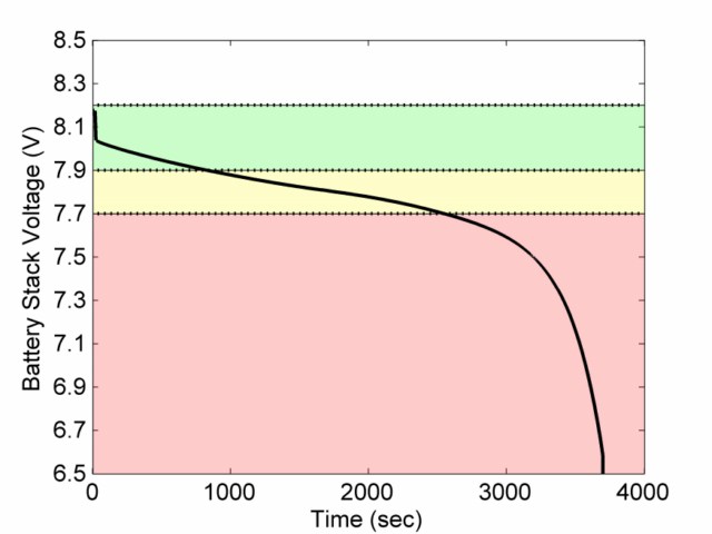
The period function is used to determine the period between wake events of the MCU. Within this function are the thresholds for the battery voltages. In the current iteration of the code, the voltage thresholds are as shown in Table 5 below. Figure 16 shows how these three operating regions relate to the discharge curve of the battery stack. Here the green section relates to the 10 sec period, the yellow the 20 sec period, and the red the 30 sec period.
| Battery Stack Condition (V) | Alarm Period (sec) |
|---|---|
| VBATT > 7.9 | 10 |
| 7.9 >= VBATT > 7.7 | 20 |
| 7.7 >= VBATT | 30 |
The caller must provide the current battery voltage, the alarm to be set (1 or 2), and the location of the delta time array (as a pointer ‘p_delta’). This array is used in conjunction with the add_time function to develop a future time to set as the alarm time.
void sleep_point(void);
The sleep_point function is used to contain the command surrounding a sleep event of the MCU. It calls up functions such as the initialization of external interrupts, enabling sleep of the MCU, calling up PRR_sleep, and putting the CPU to sleep. When the system is awoken by the external interrupt this function will disable sleep of the MCU and will call the PRR_wake function. This function then returns to the function from which it was called.
uint16_t swap_endian16(uint16_t number);
This function can be used to swap the endianess of a 16 bit uint16_t. It is no longer used in the final version of the code.
uint32_t swap_endian32(uint32_t number);
This function can be used to swap the endianess of a 32 bit uint32_t. It is no longer used in the final version of the code.
void save_data (uint32_t JD, double JD_frac, double measurement);
The save_data() function is use to contain all the functions necessary to save a data point to EEPROM. This function takes a Julian date (JD), a portion of the day (JD_fraction), and the double measurement to be recorded. The function then reads the current memory location from EEPROM. If the value is larger than 4084, the value is reset to 27 so that new data is written over the oldest data in the memory. The function then saves the Julian date, fraction of a day, and the measurement. The total space taken up by each recording is 12 bytes. The function then increments the current memory location by 12 in EEPROM so that it knows where it last left off.
Results
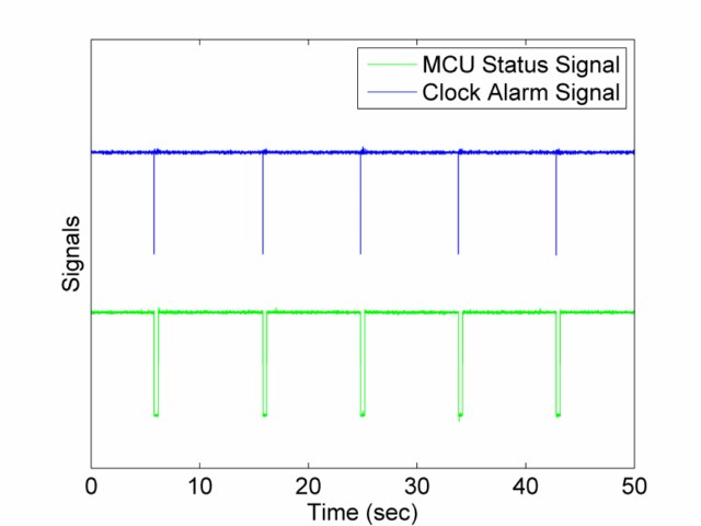
For the microcontroller system, the ability to go in and out of a deep sleep mode using an alarm from the DS1337 is key. The output from one of the pins of the MCU is used to determine which state the system is in. When the signal is high, the system is in its sleep mode, when the signal is low, the system is active. Figure 17 shows the alarm signal from the DS1337 (in blue) along with the output status signal from the MCU (in green). When the interrupt pin on the clock goes low, it triggers a hardware interrupt on the MCU to wake it up. The test results show that this operation was completed successfully.
The next bit of functionality needing testing was the voltage measurement capabilities of the MCU and the logic which used this voltage measurement to dictate the frequency of the measurements. Figure 18 shows the measurements downloaded from the MCU's EEPROM where the output from a DC power supply was used to simulate the battery pack. For each of the three different voltage levels, different frequencies of measurement can be seen, showing the successful operation of not only the voltage measurements, but also the logic which will start putting the MCU to sleep for longer lengths of time when less energy is available for the system.
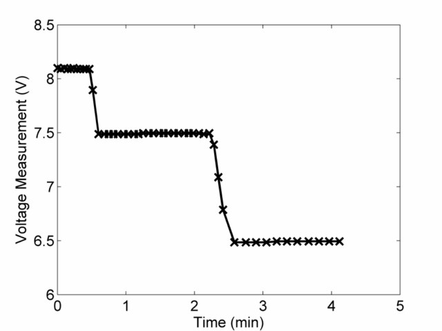
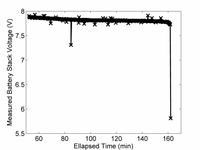
Figure 19 shows the results of indoor testing of the system without the solar cells and only the batteries acting as a power source. These results illustrate the successfull operation of the system when lacking the ability to recharge the system, where the capacity of the batteries slowly decreases as shown by the measured battery stack voltage. Figure 19(a) shows a sharp decrease in the measured voltage down to below 6 V for the last data point collected before the MCU lost all power. This behavior was shown consistently in all tests where the batteries were allowed to drain until the MCU stopped operating. This leads credibility to the argument that one of the two batteries dropped below the 2.7 V minimum allowed by the LTC4071 and was disconnected from the system overal, as mentioned in the section on Hardware Design.
 |
 |
| (a) | (b) |
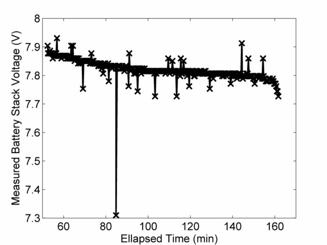
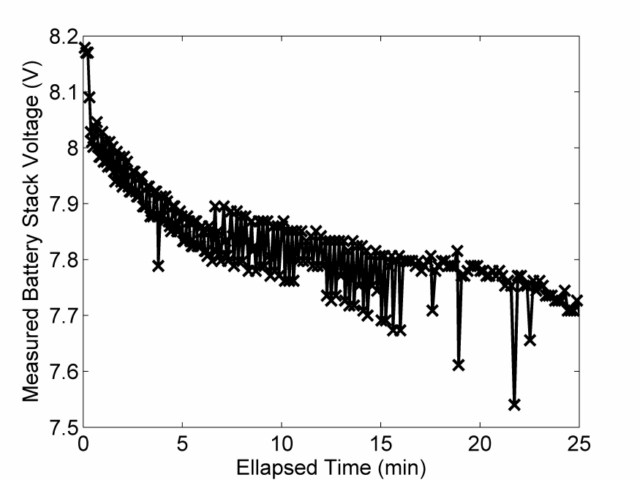
During one of the tests when we had shorter sleep periods for each of the MCU logic states, the measured battery stack voltage clearly showed the effects of being measured at different rates. The significant oscillations in the battery voltage during this test is visible because of the fast frequency of the battery being disconnected and connected to the MCU load using the high-side switch. The battery does not have enough time to settle back to its loaded steady-state voltage before the load is disconnected again. During the first period of the test, up until about 7 minutes, the oscillations were at a high frequency when we're checking the battery O.C. voltage every 3 seconds. From about 7 minutes until 17 minutes, the battery voltage was very close to the programmed threshold voltage and oscillated between measuring every 3 and 5 seconds. After the 17 minute mark, the system settles into the 5 second measurement period mode and the oscillations decreased significantly. This data not only shows the successful operation of the MCU logic modes, but the successful operation of the high-side switch as these oscillations would not have occured if the batteries were not successfully disconnected from the load.
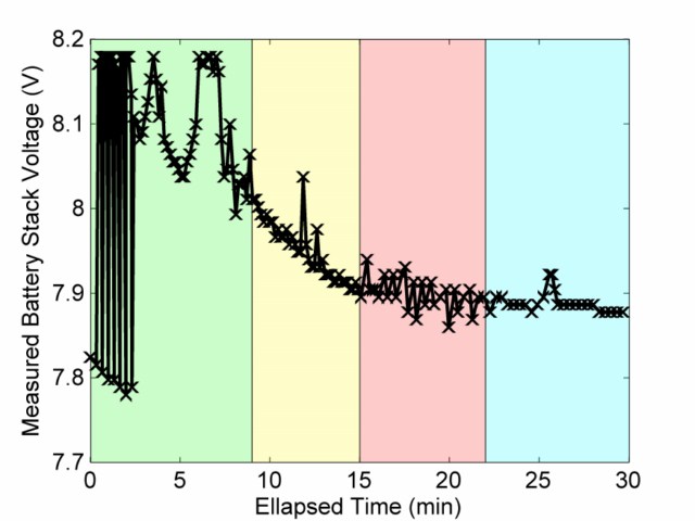
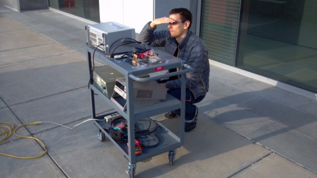
We were able to get a small amount of sunlight during the evening hours (even in Ithaca!) to demonstrate the system's ability to operate on solar power. Figure 21 shows the results of this test. For the green shaded portion of the test, the system was outside in partly-cloudy evening sunlight. The batteries that were attached to the system were not fully charged at this point. As the measurement was made, when the batteries were disconnected from the system, the oscillations in the first couple of minutes were due to the solar cells alternating between periods of producing enough power to charge the batteries. In more constant and overhead sunlight, the battery measurements should be consistently closer to the 8.2 V maximum dictated by the LTC4071's. The yellow portion of the test was when Michael thought he was a window, and stood in front of the cells. This mimiced periods of the bird carrying the tag perching on a tree out of the sun. The battery started to discharge at this point, dropping down to the 7.9 V threshold to change to 20 sec intervals for measurements. During the red portion of the test, Michael realized he's not actually made of glass, but it was very cloudy at this point and there was not enough solar power available to power the system or recharge the batteries. As a result, the batteries continued to discharge. During the cyan portion of the test, there was some reoccurance of sunlight, but not enough to recharge the batteries as we were getting pretty close to sunset at this point.
 |
 |
| (a) | (b) |
Conclusions
The final system design for this project proved to have much of the functionality we originally intended at the outset of the project. We are able to take data, manage our battery charge, put the system into deep sleep modes, charge the batteries from an ambient source, and keep track of time over long periods. The system meets the basic goal we set for ourselves at the beginning of the project. Because this is part of a larger and ongoing research and technology development effort for the bio-logger system, there is additional functionality we plan to incorporate in the coming months. Some of this functionality includes:
Wireless data downlinking
Wireless clock setting
Piezoelectric based vibrational energy harvesting
Use of the program flash memory space for data storage
Control of measurements using external sensor
Much of these increases in functionality are simply improvements to the current system. Use of the program flash space would drastically increase the number of measurements that could be taken. Additionally, the ability to wirelessly download data and update the clock would be extremely valuable as it would allow for data transfer from the animals without capture. While the system currently works, there is a small bug in the system that will be resolved in subsequent version of the code. This issue is that the fraction of a day converted by the Julian date conversion code is often one second short due to the floating-point method of variable declaration and the number of significant digits needed to maintain fractions of a second accuracy. In hindsight, we should have simply multiplied the fraction of a day by 1,000,00 and saved it as a long integer. This would resolve the issues with seconds resolution. This error can be observed in the alarm wake up times which are occasionally one second less than what is specified in the period() function.
While there are no known standards for which this system must abide, there are a few which will apply when the research project for this bio-logger nears completion. These include the IEEE 802.15.4 standard for low-rate wireless personal area networks. We will likely be using Zigbee communication protocols that are based on these standards. Additionally, we will need to consider regulations concerning the banding/tagging of birds in the United States. The US Geological Survey is entity responsible for regulating bird banding in the US. They specify that a band or tag may weigh no more than 3% of the mass of the bird to which it is attached. Neaf-Daezner et al. showed that payloads of 3-5% could be tolerated on the coal tit (periparus ater) and great tit (parus major) without affecting survival rates. The USGS has permitted up to 4% of the mass of the bird, so we will have to limit our system mass to 3-4% of the mass of the yet to be determined target species.
The majority of the code for this project was completely original. We did use various libraries with AVR Libc. These include inttypes.h, stdio.h, stdlib.h, eeprom.h, sleep.h, wdt.h, and delay.h. In addition to these libraries, we also used a library created by Paul Fleury. This I2C master library contains various commands that are used to communicate with peripheral devices across the I2C bus. Both this library and GCC Libc are in the public domain, and our use can be considered fair use.
With some improvements, we believe there are both some patent and publishing opportunities for this technology. Such a system could easy developed as a power control peripheral to almost any remote date acquisition system. With some added functionality the design could, in addition to powering down the MCU, shut down some power intensive sensor. With these improvements the technology could be used in various applications. As for publishing opportunities, we plan on developing two articles based at least partially on this project. We plan on publishing a paper comparing our battery management circuit to that of active charge management circuits. We also plan on developing a paper for the bio-logger system as a whole, and discussing power management and power harvesting from a system design standpoint.
Throughout this project we have attempted at all times to comply with the IEEE code of ethics. In addition to not taking a single bribe (admirable considering the pittance of our salary), we have improved the understanding of this technology. Furthermore, we have honestly presented the results of our work to the best of our abilities, and have specified its limitations wholly. Throughout the project we looked for honest external criticism of our design from both the instructor and our peers. We did this such that the design would be improved. Additionally, we have stated when and where designs and code have been used directly, or modified from a similar version. While we have attempted to comply with all the items listed in the IEEE code of ethics, we have violated item 6. This item states that we should “undertake technological tasks for others only if qualified by training or experience, or after full disclosure of pertinent limitations.” Our pertinent technological limitation and lack of experience should have been more fully conveyed at the start of the project. That being said, we now have this experience and would no longer need to make such a disclosure. Thanks Bruce!
Appendix
Datasheets
- ATmega128RFA1
- ATmega128RFA1 Development Board
- DS1337 I2C Serial Real-Time Clock
- 32.768 kHz Crystal
- LTC3588 Piezoelectric Energy Harvesting Power Supply
- LTC3588 Development Board
- LTC4071 Li-Ion/Polymer Shunt Battery Charger System with Low Battery Disconnect
- Infinite Power Solutions Thinergy MEC220 Thin Film Battery
- Spectrolab Triangular Advanced Solar Cell (TASC)
- RHP020N06 N-Channel MOSFET
- 2N54597 N-Channel JFET
Cost Details
Note that this project was part of an outside research project, so the budget restrictions do not apply. Also included in this budget are estimated labor expenses.
| Component | Manufacturer | Part Number | Vendor | Quantity | Unit Price |
|---|---|---|---|---|---|
| Microcontroller | Atmel | ATmega128-RFA1 Development Board | Sparkfun Electronics | 1 | $54.95 |
| External Real-Time Clock | Maxim | DS1337 | DigiKey | 1 | $2.46 |
| 32 kHz Crystal | CFS206-32.768KEZB-UB | Citizen Finetch Miyota | DigiKey | 1 | $0.49 |
| Li-Ion/Polymer Battery Charger | Linear Technology | LTC4071 | DigiKey | 2 | $4.92 |
| Thin-Film Micro-Energy Cell | Infinite Power Solutions | Thinergy MEC220-4P | DigiKey | 2 | $14.43 |
| Thin-Film Micro-Energy Cell | Infinite Power Solutions | Thinergy MEC220-3S | DigiKey | 2 | $9.02 |
| Energy Harvester Breakout | Linear Technologies | LTC3588 | Sparkfun Electronics | 1 | $29.95 |
| High Efficiency GaAr Solar Cells | TASC | Spectrolab | Spectrolab | 4 | $2.50 |
| Parts Total | $154.59 | ||||
| Labor | Slave | Graduate School | Cornell Sibley School of Mechanical Engineering | maximum reportable 400 man-hrs | $30/hr |
| Total | $12,154.59 |
Standards
- Intel HEX Standard
- IEEE 802.15.4 standard for low-rate wireless personal area networks
- US Geological Survey regulation on Bird Banding
References
- International Astronomical Union General Assembly, "On the Use of Julian Dates", The XXIIIrd International Astronomical Union General Assembly, Resolution B1, Jan. 1, 2001 [Online: Accessed April 10, 2012].
- Fleury, P., "I2C Master Library," 2005 [Online: Accessed April 10, 2012].
- United States Navel Observatory, "Converting between Julian dates and Gregorian Calendar Dates," 2011 [Online: Accessed April 29, 2012].
- Fliegel, H.F. & van Flandern, T.C., Communications of the ACM, Vol. 11, No. 657.
- United States Geological Survey, "How to request auxiliary marking permission," 2011 [Online: Accessed February 28, 2012].
- B. Naef-Daenzer, F. Wildmer, and M. Nuber, "A test for effects of radio-tagging on survival and movements of small birds," Avian Science, Vol. 1, No. 1, pp. 15-23, 2001.
- Barbenhenn, G.H., "True Grid Independence: Robust energy harvesting system for wireless sensors uses piezoelectric energy harvesting power supply and li-poly batteries with shunt charger," LT Journal of Analog Innovation, Oct. 2010.
Division of Labor
| Alexander Schlichting | Michael Shafer |
|---|---|
|
|
| Joint | |
|
|