The Design
High-level Description
We used the camera module provided by Terasic to capture two frames of images and stored them into SDRAM. To store both images in the SDRAM, we split the SDRAM into two partitions. Before we stored them into the SDRAM, we converted the images into black and white. This was to conserve temporary storage, for both SRAM and registers, and to speed up the compiling and synthesizing time. Also, because the camera was natively only one CCD, the conversion did not lose more content. Since we expected that the number of logic elements required to compute all partitions was too large for our FPGA, we decided to select the search area and reference box to be in the middle of the screen and only worked in this search area to demonstrate that our design was fully functional. It could be scaled-up to compute the full image if we have more resources. Instead of drawing a straight line, we outlined the entire search area and shaded the box with the minimum sum of absolute differences within the search area to see the output more clearly. The data for the outlines were not written back to the SDRAM. Instead, we just added the outline to the image when writing to the VGA buffer in SRAM. When we completed the design, we expected to see a black and white image with two outlines in the middle of the screen, and the smaller box would move around to track movement. Please refer to the Results section for more information. Figure 1 below is a schematic for the algorithm, and Figure 2 is a high-level block diagram for the design.
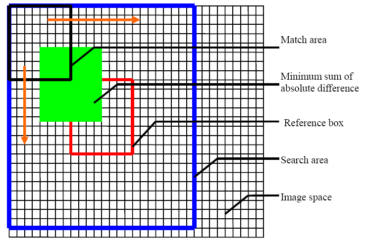
Figure 1: The implemented algorithm
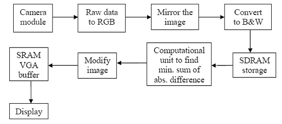
Figure 1: A high-level block diagram
Camera Module
The camera module we used came with a driver that was set up properly to capture images using a CMOS sensor. The data was processed, stored in SDRAM and sent to the VGA buffer, an SRAM, to display the image on screen. The driver helped us capture the images easily. The following is a picture of the setup:
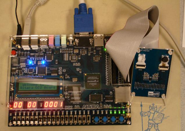
Figure 2: An Altera DE2 board with camera module
The line buffer in the provided driver would read raw data from the sensor. The CMOS sensor would produce a raw data like the diagram in Figure 4, where each pixel would only contain one component of red, blue, or green. Since the intensity of green should be twice the blue and red, there are twice as many pixels of green than blue or red. This is commonly referred to as the Bayer representation. However, the VGA display needs all three components in one pixel to display properly, so the pixel stored in the SDRAM would be a combination of all three components. Depending on position of the pixel, the combination of colors would be different. To determine the component contents, we would first need to scan in two lines from the camera keep track of which four pixels to look at, and the extract the data and put them into the SDRAM. More information about the camera and how it works can be found from the documentation of the device here. The following code was used to determine the component of each pixel (provided by driver):
:
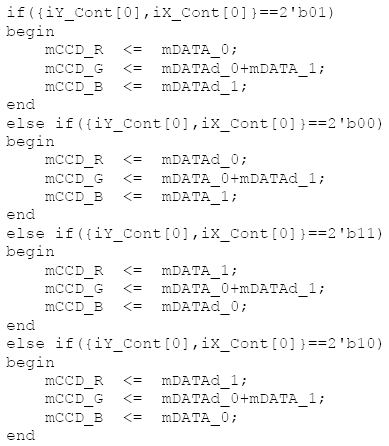
Figure 3: codes to determine the components in each pixel in SDRAM
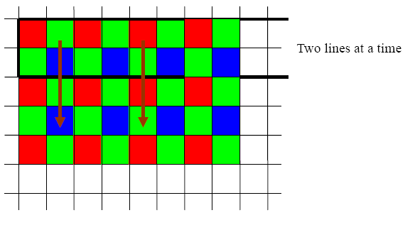
Figure 4: A schematic for Bayer filter
Memory Setup
We used both SDRAM and SRAM for this system. A FIFO SDRAM was used to store the data from the camera, and the SRAM was used for VGA buffer before the image was sent to the VGA display. The SDRAM controller took in a starting address, an ending address, a clock and the length of the data stream. The controller would then fetch data from or write data to the specified address on each clock cycle. Since we wanted to store two images into the SDRAM, we needed to partition the RAM into two sections. The size of the picture is 640x512, and the starting address of image 1 was set to 0, so the starting address of image 2 was set to 22’h100000 (a lot bigger than needed) to avoid overwriting the first image. The length of the data stream was 256. Therefore, the Verilog code for writing and reading the FIFO SDRAM looks like the following:
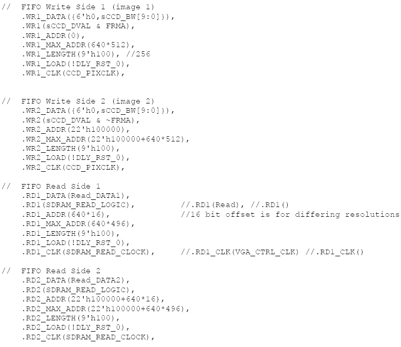
Figure 5: FIFO SDRAM controller connection
The SRAM was used to buffer output image for the VGA display. SRAM could be accessed by specifying the address and the data, without accessing data in order, which is much easier to access than the SDRAM. After we computed the minimum sum of absolute differences we needed to modify the image by overlaying the outlines on the original image. We could do this by setting the new 16-bit data to the SRAM when we went through each pixel and updated the buffer at the corresponding address during synchronization. A special feature was introduced here. We were able to draw the boxes in color though our image was in black and white. This was achieved by concatenating the 10-bit black and white information with 6-bits of color information with only one of the 6 bits being high. Therefore, the colors would become more noticeable when the neighboring pixels were darker, and less noticeable when the neighboring pixels were brighter. Essentially, if the search area was black, all three colors would show, but if the search area was white, no color would show. The following code was used to draw the red outline for the reference box to the SRAM after the computation was complete:
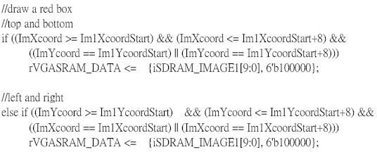
Figur 6 : codes to write the red outline to the VGA buffer
Computation
After the data was stored in the SDRAM, and the reference area and search area were defined, we would extract the data from all the pixels within both areas and put them into 10-bit registers on the FPGA. Then we compute the sum of absolute difference between the reference box and the candidate match area. With our definition, it would take 16x16 = 256 cycles to complete the entire computation since our search area was 24x24 and the reference area was 8x8. To compute the absolute difference between two pixels in hardware, we first compared the values of the data, and then we subtracted the smaller one from the larger one. After we compute the first iteration, we kept sum and a temporary register, and every iteration, we compared the sum with the temporary register to keep track of which match area in the search area has the smallest sum. When the entire search area had been gone through, a flag, doneproc, was asserted and the state became "done." The state machine was used to help control the sequence of events happening. We only compared the two most significant bits of the data because the noise floor was quite high and the information after the third bit was not helpful for comparison between the two data but made the number of logic elements increase by a lot. In this case, if we performed a Gaussian filtering, we could increase the signal-to-noise ratio, and we could detect motion in images that have less intensity contrast. However, due to time constraint, we were not able to include that in our project.
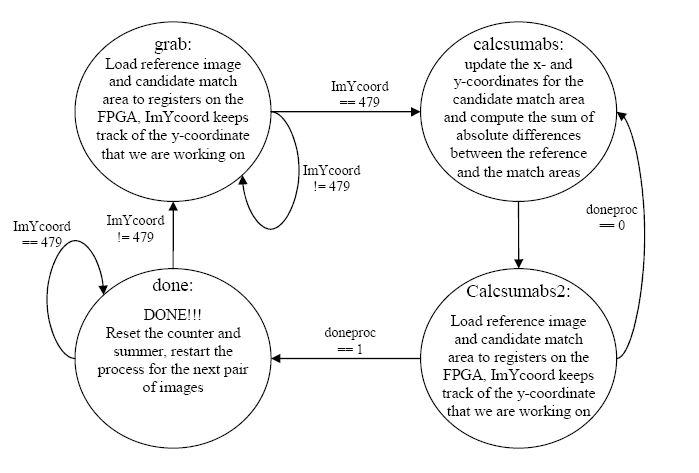
Figure 7: The state diagram of the computation stage
VGA Display
To use the VGA output on the DE2 board, we used to use the controller that came with the DE2 board. When the “sync” bit was set, the controller would output the in the VGA buffer onto the screen. The VGA buffer was an SRAM that contained 10-bit RGB data. Since we were only using grey scale for simplicity, we only needed one SRAM to display. After the computation with the done, the pictures needed to be mirrored before writing to the FIFO SDRAM in order to get the correct image when reading out the data. Essentially, we modified the VGA driver that Professor Land wrote in his DLA code to help work with SDRAM.