Matrix multiplication is a traditionally intense mathematical operation for most processors. Despite having
applications in computer graphics and high performance physics simulations, matrix multiplication operations are
still relatively slow on general purpose hardware, and require significant resource investment (high memory
allocations, plus at least one multiply and add per cell). We set out to design an FPGA-based accelerator to not
only speed up the operations, but also allow offloading of the execution to free up general processor time for
other tasks. As an added bonus, accelerators, because they don't contain any processing elements that aren't
necessary, typically are more efficient at the task at hand, requiring less power to run than a general purpose
implementation.
High Level Design
For this final project, we evaluated two very different matrix multiplication approaches. One used registers to
store the two input matrices as well as the output matrix, which allowed us to use massive parallelization,
while the other used a more scalable approach that made use of the onboard M10k memory blocks to store the
matrices. The design using registers (referred to as the register-based design) allowed any value to be accessed
with zero cycles of latency, and any combination of the values could be accessed at the same time. In the M10k
approach, we could only request a single value from the M10ks at a time due to the single read port on M10k
blocks, which would have been a significant bottleneck in a parallel structure. Below, we will discuss first the
register-based approach, and then we will go through the M10k-based approach after.
For the register-based approach, we wanted to create a design that would be able to perform matrix
multiplications in as few cycles as possible. To this extent, we realized that each value in the output matrix
could be calculated completely independently, since each value in the output matrix only depends on one row in
m1 being multiplied with one column of m2. To take advantage of this massive parallelism, we needed to store our
matrices in a data structure that allowed us to write many values into the output matrix simultaneously, and we
needed to be able to read many different values from our input matrices simultaneously. This was the reason we
decided to implement this data structure from registers. The overall design can be seen below in Figure X:
Figure 1: 2x2 Example of Register-Based Design
Essentially, each value in all three of the matrices was stored as an 18 bit register. In Figure 1, we can see
that m1, m2, and res all consist of four 18 bit registers each (each box is an 18 bit register), but this would
scale to requiring 3*n2 18 bit registers in the case where we were multiplying two nxn matrices. As
for the
multiply accumulate units (MACs), we designated one mac per value in the output matrix. As can be seen above,
this meant that each MAC needed access to one row in m1, and one row in m2. Since we were using registers to
store all these values, each MAC had access to any value it required with no latency, regardless of what the
other MACs were doing. This was crucial for parallelization, because this allowed us to take n cycles total to
calculate an nxn matrix multiplication. However, one can easily see the problem associated with this design,
both the registers and the MACs scale with n2, meaning that for a larger design, significantly more
hardware is
required. We see this solution as more of a specialized implementation that would only be used when matrix
multiplication was crucial to the operation of a system, and the size of the matrices were small. Perhaps, one
use case would be in computer graphics where it is common to find 4x4 matrices being multiplied and these
actions must be repeated very frequently.
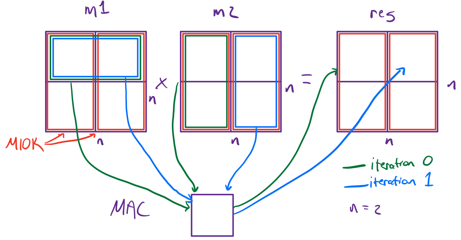
For the M10k-based approach, rather than having one register per value in all three matrices, we opted
for
having n M10k blocks per matrix, where each M10k block can be thought of as a column of values within the
matrix. Since M10k blocks only have a single read and write port, it is not possible to exploit as much
parallelism as in the register-based approach. If we were to create one MAC per output value as we did in the
register-based approach, we would not be able to serve each MAC the value it needs to calculate its output, and
the MACs would largely sit idle, waiting for their value to be read out by the M10k blocks. Instead, we decided
that we would see more performance if we were to keep the hardware simpler and then try to increase the clock
frequency. For this reason, we decided on having a single MAC, as can be seen below in Figure 2:
Figure 2: 2x2 Example of M10k-Based Approach
We hoped to achieve better 'single threaded' performance by increasing the clock frequency and pipelining the
multiply-accumulations as much as possible with this scenario.
We compare both of these solutions to a simple implementation of matrix multiplication written in C.
This is a
straightforward O(n3) implementation that essentially performs the same operations as the hardware
does, which
can be seen in Figure 3. This gave us an interesting comparison because while the ARM HPS is running at almost
10x the clock frequency of the hardware we designed, there is far more overhead for any given instruction
running in C than in the hardware. For example, in the C code, there are branches for the for loops that must be
predicted and resolved, there are cache misses that would require far more cycles to retrieve a value from main
memory, and loads and stores cannot happen simultaneously to each of the matrices. So, if our hardware were to
keep up with the HPS, it would have to be far more efficient, taking full advantage of each cycle.
Figure 3: C Code Implementation of Matrix Multiply
Program & Hardware Design
The main part of both of our implementations was our MACs. These MACs were quite simple in design, consisting
of a multiplier and an accumulator. When the MAC was told that it should be running, at every clock cycle, it
would take the value from the multiplier and add it to the current accumulation value. One of the more
challenging parts of the design was making sure that these MACs were fully utilized in both of the designs. For
the register-based implementation, it was quite easy to fully utilize the MACs, as each could access values
independently of one another, and there was no memory bottleneck. Because of this, right after the HPS finished
programming each register with its value for m1 and m2, we knew that in 15 cycles, there would be an output read
in the res registers. Each of the MACs ran at full force, updating its accumulate variable each cycle. In the
M10k-based design, this was slightly more challenging. M10ks have a one cycle read latency, meaning that when a
value is requested, it will not be available until the following cycle. This meant we had to ensure we pipelined
our requests to the M10ks such that on the next cycle, the M10k would be responding with useful data, and we
would be ready for this data. In this way, we only lost the first cycle of each iteration, rather than doubling
the number of cycles required to interact with the M10ks. Additionally, because we used separate M10ks for m1
and m2, we were able to do reads to each separately, meaning that on every cycle, we would have data from both
of the input matrices that we could use in our MACs.
As for our Qsys implementation, we used many different PIO ports as well as a PLL for our multiplier
hardware. The PIOs gave the FPGA information about the data that the HPS wanted the FPGA to respond with, data
about initializing the matrices, and data about the size of a given input matrix. PIOs were also used to send
data from the FPGA hardware to the HPS, including the status of the multiplications or the value at a certain
index in the output matrix. These PIOs gave us high speed communication between both entities that allowed a
close hardware-software codesign. The PLL was used to create a phase-locked generated clock that would run all
of the matrix multiplication hardware. When trying to change the clock frequency we were operating at, we would
change the desired output from this PLL, which caused many problems and is discussed in more detail below.
While our multiplier was configured such that it could handle up to a certain size matrix (ie in the
register-based implementation 15x15 and in the M10k-based implementation 80x80), we configured the hardware such
that two matrices that were smaller could still be multiplied. Beyond this, the hardware would require fewer
cycles for the M10k-based implementation depending on the input matrix size. Essentially, we would pack the
matrices into the upper left corner of our M10k data structure, and then the result would end up in the top left
corner of our output matrix. Rather than calculating all of the multiply accumulations that would result in
either 0 or in values that we did not care about, we told the hardware what size the input matrix was, and then
the hardware would only calculate the required values.
Another interesting part of the design was the handshake we used between the FPGA hardware and the C
code. In previous labs when timing wasn’t as important, we would simply use sleeps in the C code to ensure the
FPGA received a message. When writing to hundreds of registers or M10k values, and with timing being critical
for our system, we wanted to get rid of the need for sleeps, which meant that we needed a handshake. Our
handshake was inspired by Cornell’s ECE 4750 and 5745 classes, where different parts of the processor would
communicate with a handshake consisting of a valid, ready, and message signal. valid and ready were used to
indicate the state of each system with respect to receiving or sending a message, and the message contained the
actual information. When the FPGA was ready to receive a message from the HPS, it would assert the ready signal.
If the HPS saw that ready was high, it would put the message into the PIO (which acted as our message signal
between the HPS and the FPGA), and then the HPS would assert valid. At this point, the FPGA knew it could lock
in the value safely. While the FPGA was processing this value, it would make ready low, telling the HPS that it
was not ready for a new value yet. This system ended up being quite effective, making it so that we could send
messages with only a cycle or two delay between the HPS and FPGA, rather than using microsecond sleeps as we had
in previous labs.
While implementing both of our hardware solutions, we ran into several problems along the way. The first
was while we were trying to implement the register-based system. We chose to work with 18 bit numbers because we
wanted to make full use of the DSP block multipliers that we learned about in Lab 2. The FPGA has 87 DSP blocks
and each has support for two hardware multipliers, which should give a total of 174 18 bit multipliers. However,
as we increased the number of multipliers for this implementation, we quickly realized that the FPGA flow was
erroring out if we tried to use more than 87 DSP blocks. With 174 multipliers, we had planned on supporting up
to 13x13 matrix multiplication, but the tool would tell us we had run out of hardware and were requesting to use
169 DSP blocks. Clearly, the tool was not allowing us to pack two hardware multipliers into each DSP block.
After searching for a solution for some time, we realized that there was another way around this problem. Rather
than relying only on DSP block multipliers, we could use the ALMs within the FPGA to implement multipliers as
well. The control logic for the hardware multiplier took relatively little area on the FPGA, so we had plenty of
ALMs left over. For this reason, we used the IP generator within Quartus to generate two different kinds of
hardware multipliers, those that depended on DSP blocks, and those that depended on ALMS. We configured our
generate statements to use 87 of the DSP based multipliers, and then the rest of the multipliers should be from
ALMs. We found that we were able to get to a 15x15 multiplier before running out of hardware, or using 87 DSP
based multipliers and 138 hardware based multipliers.
While implementing our M10k-based implementation, we ran into problems when trying to increase the clock
frequency in order to increase the ‘single threaded’ performance. At 50MHz, our hardware worked well, but we
were hoping to decrease the computation time, so we bumped this up to 100MHz. Seeing a large performance
improvement, we wanted to continue to increase this so that, ideally, we could perform even faster than the HPS.
However, we started running into problems after we pushed the clock past 100MHz. Rather than reading out correct
values from the matrix multiplication, values were volatile, changing every time we ran the code. To us, this
seemed indicative of either a clock domain crossing that was not being handled properly or a design that was
failing its timing constraints. Looking at the timing results, we were indeed failing timing, but the tool was
telling us we were failing paths by tens of nanoseconds, which usually means that there are unconstrained paths
that the tool is simply timing incorrectly. In general, we failed timing on every lab due to these types of
unconstrained paths, so it was unclear whether or not timing was causing this issue. As for clock domain
crossings we tried to keep our clocks at integer multiples of one another, we generated all of our clocks using
PLLs based on the same source clock, and we used a simple form of handshaking to know whether the other clock
had received our message. For this reason, we believed we had handled any clock domain crossings correctly. In
the end, we concluded that the random values were likely due to a failed timing constraint, or an unconstrained
path that was failing setup or hold timing, so we decided to keep the clock frequency at 100MHz. Running our
multiplier hardware at 100MHz gave us execution time of approximately equivalent to the HPS, so we still had an
effective accelerator that would do the same amount of work in approximately the same amount of time, but at a
lower power and with a higher degree of certainty as to when the multiplication would finish. If this
accelerator were implemented with a processor, the effective throughput could potentially double, as the
accelerator could perform multiplications at the same time the HPS is. On our last attempt to increase the clock
frequency, we actually managed to crash linux running on the HPS, and could no longer access the FPGA via ssh.
As for the C code, we had a very straightforward implementation. Essentially, the code would tell the
hardware that we wanted to initialize m1, and then it would iterate through all the indices of m1, telling each
value to store in that location. Then, we would switch to m2 and repeat this process. After this, we would tell
the FPGA that it had all the required information at which point the C code could simply wait for the hardware
to finish. When the hardware was done, it would set a bit, indicating this to the HPS. Then, the C code would
request each value out of the result matrix, printing line by line so that we could confirm the answer was
correct. As mentioned before, we were able to speed up this code significantly by removing any waits and using
the handshake to determine when the hardware was ready for a new value.
Results and Evaluation
To verify that our solution ran as expected, we simply printed the output matrix of each case and verified it
with a custom Python script that naively calculated the desired value for each cell. We then introduced timing
information into our wrapper code pieces and aggregated the results using a shell script and Python for result
parsing.
On the quantitative side of our evaluation, we ran 8000 tests, 1000 of each the baseline
(HPS-only)
implementation and our accelerated implementation, for four different matrix sizes, 20x20, 40x40, 60x60, and
80x80. We then compared the statistical data between the implementations, including mean, median, and standard
deviation, as well as tail latency metrics.
Figure 4: Results Summary, Runtime vs. Test
We see from the results summary chart that while our accelerated implementation does not outperform that of the
naive HPS implementation in most cases, the accelerated mean typically ranges within 10-30% of the median
HPS-based
implementation's runtime. We also see interesting characteristics displayed by the accelerated solution. Since
our
implementation takes a predictable amount of clock cycles per matrix multiply operation, we see that while the
measured latency is not exactly the same per run, the distribution is much more uniform when compared to the
extensive tail effects of the HPS. This predictability can mean quite a bit when designing code to run around
the
accelerator, and can lower process variability in certain situations.
Additionally, it's important to note that our tests were entirely conducted using a 100 MHz clock for
our
accelerator. While we weren't able to completely flush out designs that ran on higher clock speeds, in theory,
the
multiply-accumulate portion of logic should be able to be clocked at least 2-5x higher than that of the initial
base
clock of 100 MHz.
We also know our HPS solution to likely be highly memory efficient. Since the maximum matrix we verified
can run
on
the FPGA implementation is 80x80, we opted to test the HPS-based solution similarly to that figure. We assume
there
are some caching effects here at play, influencing our end result. An 80x80 matrix contains 6400 values, stored
as
integers, which are represented as 4 bytes of data. The entire matrix therefore contains just over 25KB of
space,
and with three matrices per run iteration, consume totally just over 75KB of memory. We know the HPS to be built
from a 925 MHz, Dual-Core ARM Cortex-A9 MPCore processor with 512 KB of L2 cache and 64 KB of scratch RAM.
While
all three matrices would fit in scratch RAM, they most definitely fit within the L2 cache, likely significantly
speeding up memory access time and latency.
Figure 5: Hardware Power Usage
Figure 6: Results Summary, Power Usage by Operation
We now present our power usage figures for each design. More than just speeding up execution time, accelerators
also present a more efficient solution to a potentially complex task, often with dedicated hardware, and as a
corresponding result, lower power usage than if the task ran on the general purpose microprocessor. We see that
the accelerator, as measured by our power estimator tool in Quartus, has a lower power usage figure, at 1.03 W
vs 1.25 W of a single core implementation running atop the HPS.
We then factor in these figures to calculate the overall energy usage for each matrix multiply
operation,
factoring the timing information for each operation and a fixed power draw according to the estimator. We find
now that, while still on average (mean and median) the HPS-based solution uses less power, the accelerator is
again more consistent, and is below the 90th and above tail data for the HPS-based solution. That is,
consistently, the accelerator uses less power than the top 10% of results using the HPS-based solution.
Conclusion
While we found that our solution didn't necessarily perform strictly faster than the HPS-implementation, we did
find that with minimal hardware usage and optimization we arrive within 25% in the average case of the HPS
implementation. Additionally, we find that we use similar power figures for each implementation. Since
accelerators also work through offloading computational load and thus freeing up processing resources, this is a
promising result--to achieve similar performance and power as the onboard processor.
Our results are also just a first step in designing such an accelerator, and as such leave significant
room for improvement. We see that the current design works with up to an 80x80 matrix at 100 MHz clock. In
theory, we could simply bump up the clock frequency of the logic portion to run at 200 MHz or even 400 MHz, in
theory improving our execution times by a factor of 2-4x.
We also note that our design could make more efficient use of the M10k memory blocks, and instead of
allocating an entire block to a given row of a matrix, we could pack the values as tightly as can be
represented, since, controlling for the value of bit width, the number of values stored in each block is a
constant--and our current scheme likely wastes free memory blocks.
We also acknowledge the caching limitation inherent in our microbenchmark. Because our accelerator uses
small matrices, we cannot efficiently scale to even greater values to push the limits of caching onboard the
HPS.
Still, given the limited amount of time we had to work on this project, coupled with the accurate and
promising results, we can mark this project in our books, as a success. We showed promising, if yet unexpected
results for the speed of computation of our accelerator, but demonstrated ease of implementability in
traditional programs. Inevitably, hardware design is never as straightforward as we initially expect, and in
this case, between optimizing for M10K memories and DSP blocks available on the development board, we spent a
reasonable amount of time understanding the limitations of our physical system and development environment.
Overall, we are quite pleased with our results and have demonstrated sound hardware/software codesign.