
Binarized Neural Network for Digit Recognition on FPGA
Vidya Ramesh and Xitang Zhao
For our ECE 5760 final project, we implemented a Binarized Neural Network (BNN) - a Convolutional Neural Network (CNN) with binarized feature maps and weights- to perform digit recognition on an FPGA. CNNs have extensive uses in image classification applications and BNNs have the potential to provide the same functionality while using fewer memory and logic resources. The project presented an interesting means by which to learn more about machine learning from a hardware perspective.
Background
Neural networks are a machine learning model based on the neural networks in the brain. A series of nodes are arranged in “layers” which are connected to each other by operations and weights. The model has shown to be successful in image classification tasks which have many applications today, from autonomous vehicles to facial recognition. Standard CNNs can have floating point weights and feature maps- these require significant memory resources and computational power to implement the necessary multipliers, etc.
Binary neural nets make use of binarized feature maps and weights, which greatly reduces the amount of storage and computational resources needed and makes it possible to synthesize them in hardware on resource constrained systems such as FPGAs. The net we implemented is based on a software model implemented in Python using the Tensorflow machine learning library. The Python code was provided by Cornell PhD student Ritchie Zhao. The Verilog code implements in hardware the various layers and functions which are used to construct the software model. The system is intended to classify digits and uses a subset of the MNIST dataset to train the model and yielded a testing accuracy of approximately 40%. This could be improved by using non-binarized feature maps and implementing additional functionality such as batch normalization. However, such features would introduce floating point values into the system, which we wanted to avoid.
The Verilog model is used to carry out inference tasks but does not train the weights it uses for computation. Instead, the weights used are generated by the Python implementation and are hard coded in the Verilog model. Training weights is time consuming and not done in real time while the neural network is being used in classification. As such, we chose to focus our model on classification tasks and use pretrained weights for the computation. We initially planned to use the HPS to pass in weights to be used by the FPGA; however, this resulted in too many logic units being used and the design did not fit on the device.
High Level Design
Mathematical Overview:
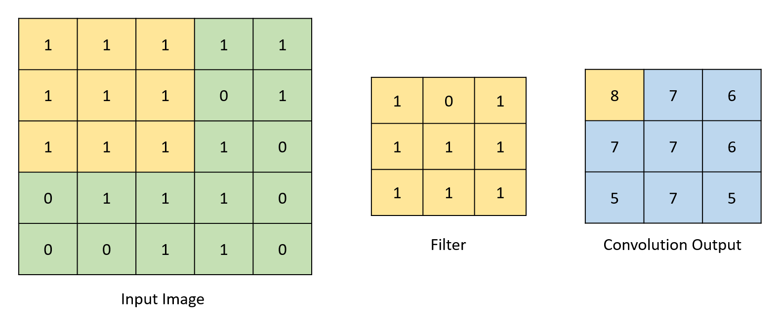
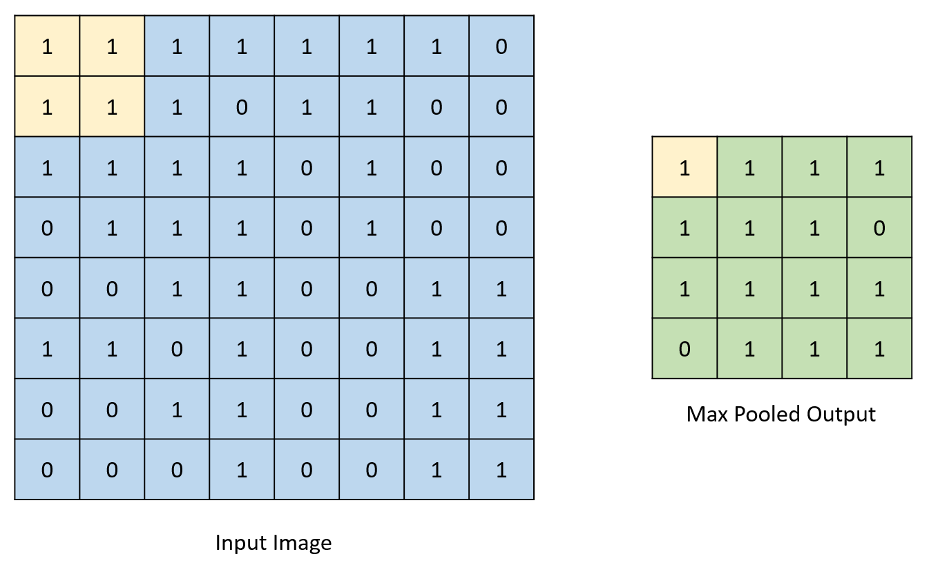
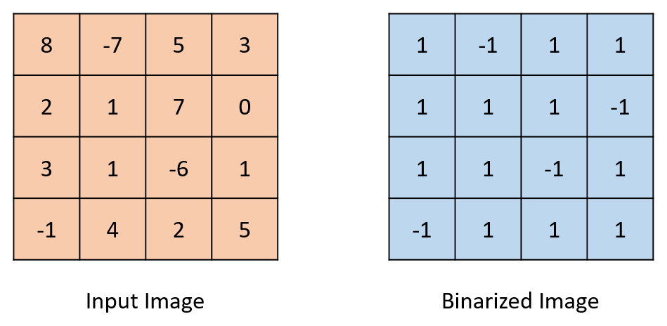
The math involved in calculation of the different output feature maps is largely limited to multiplication and addition operations. Since the weights in our design are binary values, multiplication operations can be replaced with ternary operators which determine whether a value must be added or subtracted after being “multiplied” by a 1 or -1 ( a weight of 0 is treated as -1). This greatly decreases the number of DSP blocks needed to implement the design. The convolution operation is performed by “sliding” the filter across the input feature map. Overlapping indexes are multiplied with each other and added to form the value at the corresponding output index. Binarization is implemented by determining the sign of the value being binarized and assigning the output value to -1 or 1 accordingly. While true binarization involves converting outputs to 1 or 0 rather than 1 or -1, the calculations required for this net make it more effective to convert to 1 or -1. For the rest of this report, references to binarization refer to conversion of numbers to 1 or -1, not 1 or 0. The pooling operations involve checking for the maximum value in a given set of values and assigning the output to this max value. The images below depict all these processes.
General Overview:
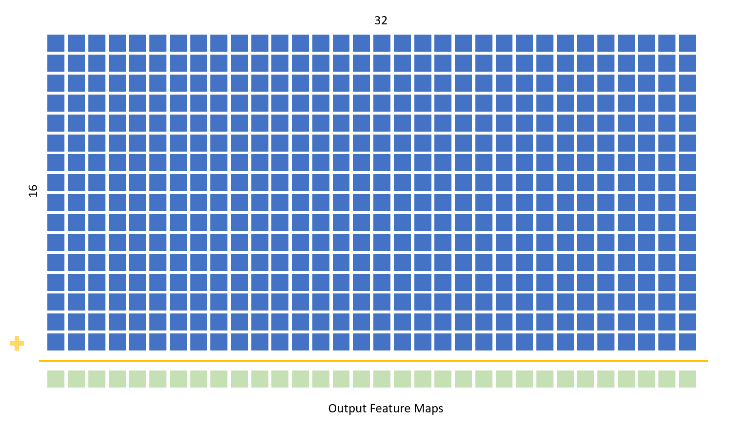
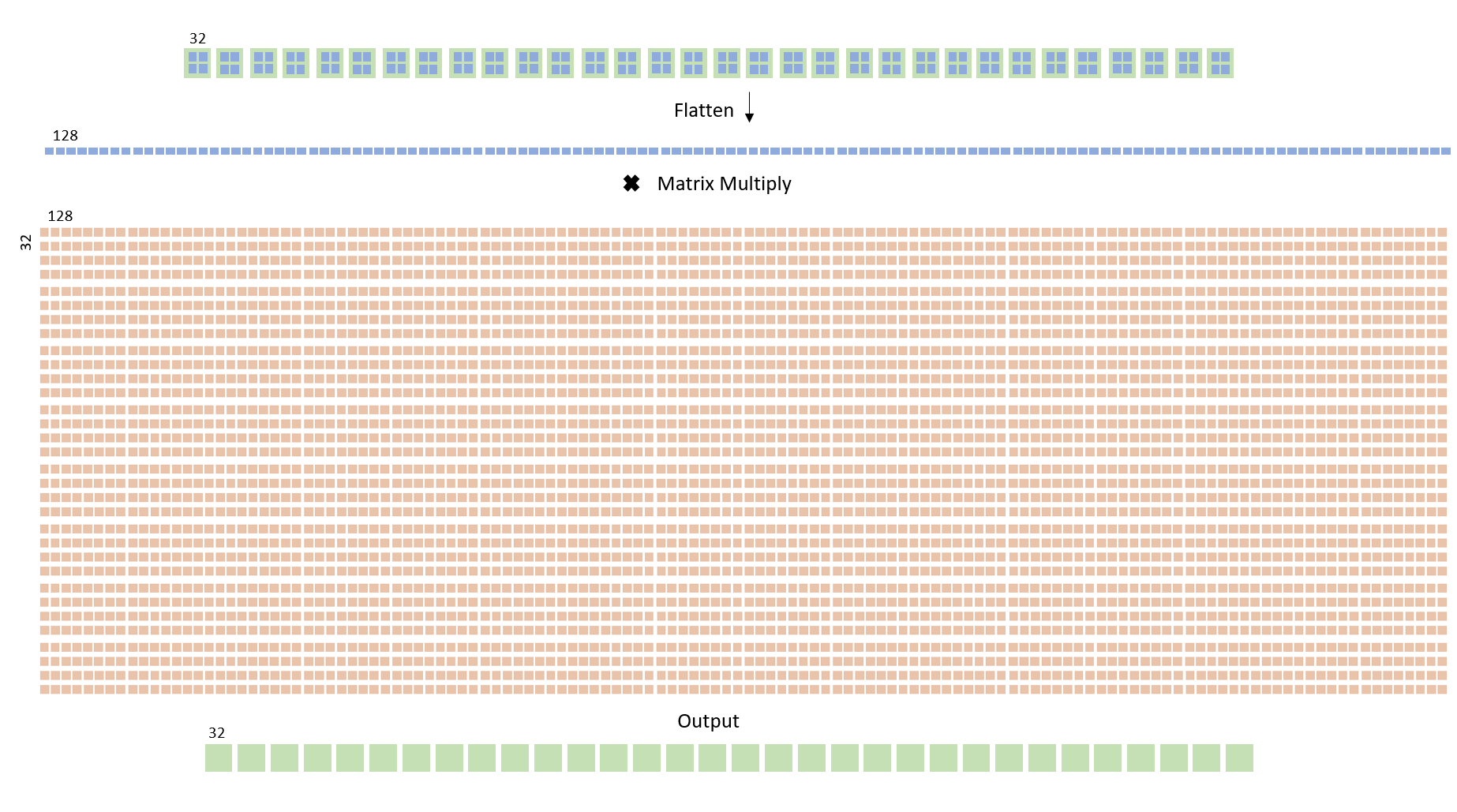
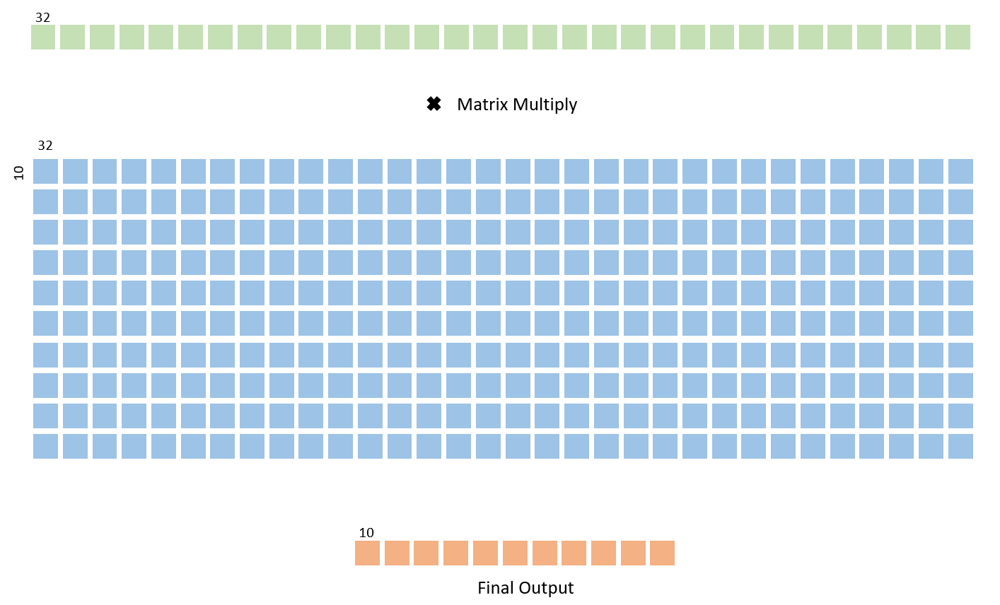
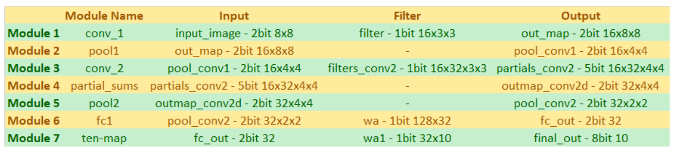
The binary neural net consists of two convolutional layers, two pooling layers, and two fully connected layers. The input image is a 7 by 7 two bit black and white image. The image is padded on the bottom and right side with -1s to create a 8 by 8 image which is fed into the net. The first convolutional layer convolves the input image with 16 3 by 3 filters to produce 16 8 by 8 output maps, which are binarized to contain only 1s and -1s. These 16 maps are then pooled to form 16 4 by 4 output maps, which are then fed into the second convolutional layer. The second convolutional layer contains 512 3 by 3 filters. Each image is convolved with 32 unique filters to produce 32 4 by 4 output feature maps. These are then binarized and pooled to turn them into 2 by 2 output maps, which are passed to the fully connected layer. The first fully connected layer flattens the incoming 32 2 by 2 feature maps into one 128 entry array. This array is then matrix multiplied with a 128 by 32 filter array to produce an output array of size 32. This output array is then binarized and multiplied by a 32 by 10 filter matrix in the final fully connected layer to produce a ten entry array. Each entry in this array corresponds to the probability that the input image was an image of the number corresponding to that index of the array. For example, the 0th entry in the array indicates how likely it was that the input image was a 0. And if 0th entry in the array has the highest value in the array, the BNNs would inference the input to be a digit 0.
All the feature maps and weight arrays were stored in registers, and the convolutions and matrix multiplications were implemented using ternary operators. Use of DSP blocks would have resulted in a shortage of multipliers needed for the design. The two bit size of the feature maps and 1 bit weight arrays led to minimal storage requirements, eliminating the need for memory units such as M10K blocks. All the weights for each of the layer were hardcoded in Verilog. We initially planned to have the HPS feed in the weights using PIO ports; however, this resulted in the use of more ALMs that were available in the FPGA.
Hardware Design
Input Image
Ten input images from the MNIST test set corresponding to each of the ten digits are hardcoded in Verilog on the FPGA. The FPGA receives an input select signal from the HPS, which is used to pick among the various images to be the input and to feed into the binarized convolutional network to generate the digit prediction output. The input images from MNIST test set are average pooled to a 7 by 7 size matrix in 1 bit grayscale. We used 2 bit for each entry because the input is binarized to be 1 or -1, with 2’b01 representing black pixels and 2’b11 representing white pixels. We then padded the bottom row and right column with -1s to form a 8 by 8 matrix before inputting the image to the first convolutional layer. This makes the matrix an even size, which is easier to work with in further layers.
VGA/Camera
Our original plan was to use an NTSC camera to capture live images or handwritten digits as inputs and to perform digit classification in real time. We started off with Bruce’s video code on the Avalon Bus Master to HPS page, which stores video input to on-chip SRAM via the Video_In_Subsystem module in Qsys, and has a bus master that copies pixel from the SRAM to the dual port SDRAM, where the SDRAM data is then being displayed by the VGA Controller module on the VGA screen. We played around with the code and Qsys video subsystem module. We were able to convert 8-bit RGB color to 2-bit grayscale, as shown in the images below, trim the input size from 320x240 to 224x224 using the Video_In_Clipper and Video_In_Scaler Qsys modules, and then create a 7x7 image on the HPS using pooling. Later, we realized this plan wasn’t feasible, as we ran out ALMs on the FPGA, which we have used most for building the actual binarized neural network. As a result, we chose to hardcode some existing input images from the MNIST dataset on the FPGA and sent over a select signal to choose various from them.
Convolution Layer One
The first convolutional layer makes use of 16 3 by 3 filters with each entry of size 1 bit. The input image is an 8 by 8 matrix with entries of size 1 bit and is convolved with each of the filters to generate 16 output feature maps of size 8 by 8. The size is maintained at the same size of the input image by padding all sides of the input image with zeros to make it a 10 by 10 matrix. When convolved with a 3 by 3 matrix, this results in an 8 by 8 matrix.
The convolutions are implemented by using ternary operators to determine whether the bit in the filter is a 1 or 0, and thus whether to add or subtract the value in the input fmap to a temporary sum. To save space, we used 1 bit weights ( 1 or 0) and ternary operators instead of two bit weights to represent 1 and -1. The temporary sums are stored in a temporary feature output This is repeated for every entry in the output feature map and takes place in parallel for each of the 16 3 by 3 filters. Once all temporary sum values are calculated, the sign bit of these is used to assign a +1 or -1 to corresponding entries in the output feature maps. Basically, we assign temporary sum to +1 if it is positive and greater than 0. Otherwises, we assign it to -1. Note that we assigned -1 to a temporary sum of 0 with this implementation. This layer is implemented using two combinational always blocks, one which implements padding and one which calculates the convolution. Each block contains nested for loops which allow for calculating all the temporary sums in parallel. In the main body of the code, a generate loop is used to implement 16 such convolutional units to allow for parallel computation of each of the 16 output feature maps.
Pooling Layers
There are two maximum pooling layers in the net, with one after each convolutional layer. The pooling layers downsize output feature maps by a factor of two. The first pooling layer converts 8 by 8 feature maps into 4 by 4 maps while the second converts 4 by 4 feature maps into 2 by 2 maps. This is done by taking the maximum value in a square of four values and assigning that value as one entry in place of all four values in the output feature map, thus reducing size. Both layers are implemented using for loops to generate hardware to simultaneously process all elements in the input feature maps.
Convolution Layer Two
The second convolutional layer is implemented in much the same way as the first. Two combinational always blocks are used to pad the image and calculate the temporary sums from the convolution, which are then stored in the output feature map. Unlike in the first convolutional block, the outputs here are not immediately binarized, as partial sums must be calculated first. The convolution of each of 16 feature maps with 32 unique filters creates 32 output feature maps for each input feature map. These 32 outputs are then summed and binarized to create 32 final output maps. In the main code body nested for loops within a generate block are used to implement all the convolutions in parallel.
Partial Sums
The partial sums layer takes in the 16*32 4 by 4 feature maps computed by the second convolutional layer and and sums up the 32 maps corresponding to each of the input 16 feature maps to the layer. The partial sums are calculated using a 32 4 by 4 cumulative temporary sum array. A state machine is used to first initialize all values in the array to 0 in the first state, and in the next state iterate through the 16 rows in the 16 by 32 by 4 by 4 array which is passed into the layer. Nested for loops are used to calculate the 32 by 4 by 4 partial sums in parallel- after 16 clock cycles in this state the partial sums have been calculated and the state machine moves to the next state. Here, the partial sums are binarized and assigned to the 32 by 4 by 4 output feature map which is passed to the second pooling layer.
First Fully Connected Layer
The fully connected layer takes in the 32 by 2 by 2 matrix outputted by the second pooling layer and flattens it to form a one dimensional 128 length array. This is multiplied by a 128 by 32 matrix to form a length 32 array. This layer is also implemented using state machine and a temporary sum array of length 32. In the first state the temporary sum values are all initialized to 0. In the next state, ternary operators are used to determine if the value in the weight matrix is a 1 or 0 and the value stored in the corresponding index of the flattened feature map is added or subtracted from the temporary sum respectively. This is repeated for 128 iterations- the number of rows in the 2D weight array. A for loop is used to implement 32 such operations in parallel. In the state after this, the temporary sum value is binarized to 1 or -1 and stored in the output feature map.
Second Fully Connected Layer
The second fully connected layer is structured in the same way as the first. It takes in the 32 length array from the previous layer and matrix multiplies it with a weight matrix of size 32 by 10 using the same state machine structure as described before. The output matrix is a size 10 array with 8 bit entries - the values are not binarized to provide more information about the classification of the number.
Software Design
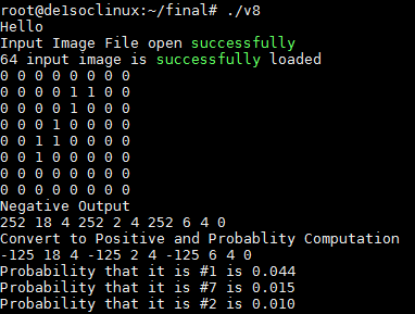
The final output of the binarized neural network is an length 10 array. The value at a given index of this final output array corresponds to the liklihood that the image that was processed was an image of that index number.For example, if the value at index 0 is the lowest value in the array, this indicates that the image processed has the lowest chance of being a 0. Likewise, if the value at index 5 is the highest value in the array, this implies the BNN has inferred that the image is most likely of the digit 5. We passed these 10 final output values from the FPGA to the HPS using an 8 bit wide PIO port. The HPS then processed the 10 final output and converted the digits to a probability scale to determine the top three most likely classifications for the image. The output from the the HPS on the serial console is shown in the image before. To calculate the probabilities, we first sum all the positive final output values to get the total sum of positive inference index. The probability of digit n can then be computed by dividing the value of the final output at index n with the sum of positive inference index.
Qsys Design
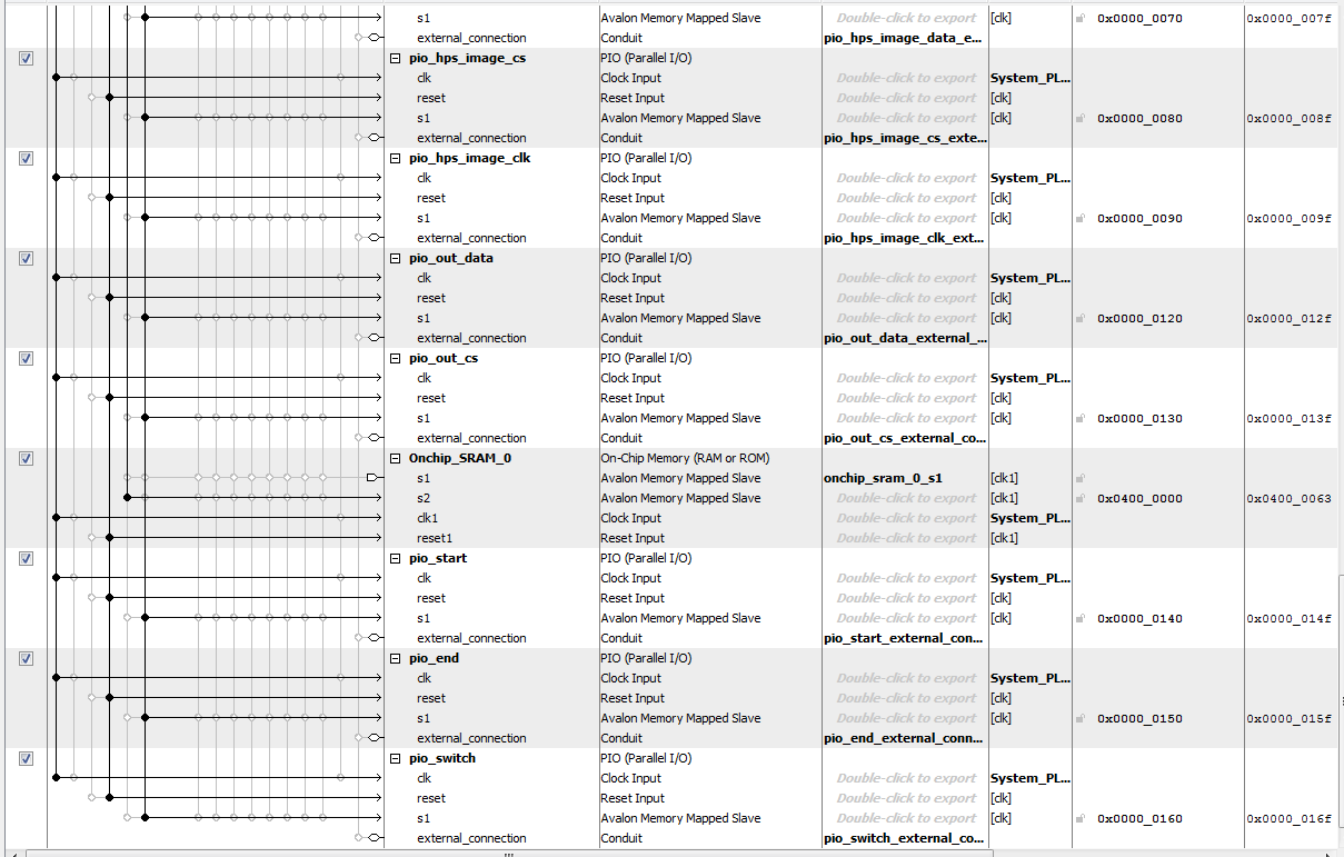
The image below shows the Qsys implementation for our design. PIO ports are connected to the lightweight axi master bus from the HPS and exported to the FPGA fabric at different memory addresses. Pio_switch is the output signal that we used to select the various input images that were hardcoded on the hps as new input for the BNN. Once pio_swich is selected and outputted to the FPGA, the HPS toggles the pio_start from low to high to restart the BNN digit recognition computation. At BNN restart, Pio_end is set to low and only set to high by the FPGA when the BNN finishes computing the final output array. By recording the time at reset and the time at which pio_end goes high, we can calculate our BNN computation time by the start and end time time difference, in which we found to be about 4-5us.
After the FPGA finishes the computation, three PIO ports (pio_hps_image_clk for clock signal, pio_out_data for data signal and pio_out_cs for chip select signal) are used to receive the 10 final outputs sequentially from the FPGA to the HPS. The chip select line is usually held low to reset the index. When the chip select is high, the corresponding index of the final output array would be loaded to the data signal on every rising edge of the clock signal. After this, the index is incremented. To start receiving the final output, the HPS pulls chip select high, toggles the clock signal, and then reads and stores the value at the data port, thus storing the value of the final output array at index 0. It then repeats this process nine times to receive all the final output array data values.
Testing
We tested initial iterations of our design on Modelsim and employed unit testing to ensure each of our modules worked as expected. We implemented each module and passed in known input values and simulated results to verify that the outputs were as expected. Once we had done this for all of the layers involved, we moved on to instantiating all the layers and connecting them to each other. We then set all the weight values and input image to known values and monitored flow throughout the net.
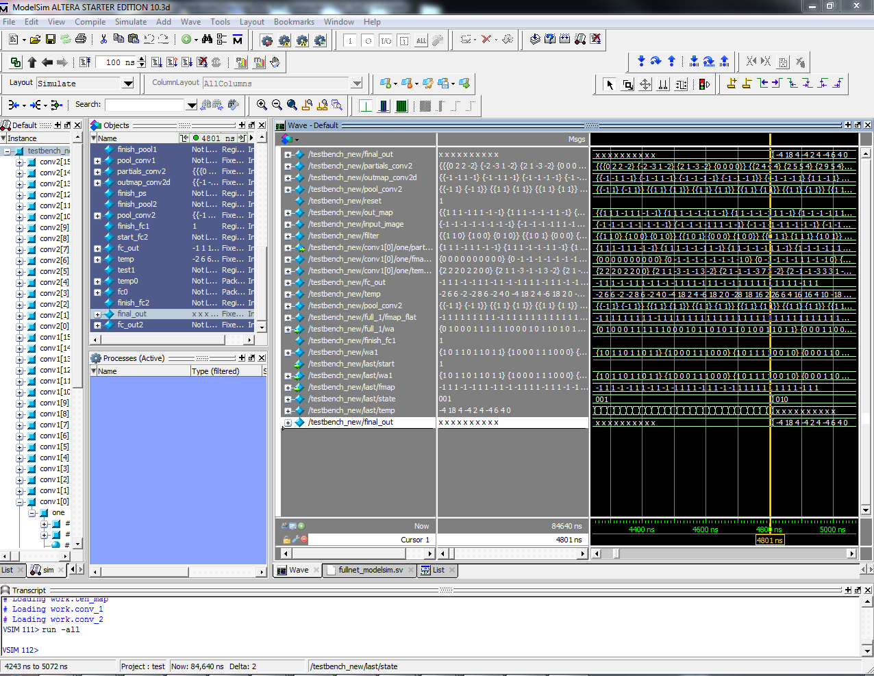
Once our design simulated correctly, we moved it onto the FPGA and used LEDs and PIO ports to look at the output of each layer to ensure that the design performed in hardware as it did in simulation. Since Modelsim only simulated parallel execution, we had to repeat all our tests with the design on the FPGA to actually verify whether our layers worked as expected. Some errors we found were parallel implementation of sequential operations, such as cumulative sums led to inaccurate calculations on the FPGA. In Modelsim these simulated correctly since execution in the software was actually sequential, but this is not the case when actual circuits are generated.
When debugging on the FPGA, the implementation of each layer was tested by mapping the output to LEDs or printing it on the serial console after sending it to the HPS through PIO ports. The hardware calculated values were compared to a software implemented Python model to verify that each layer functioned as expected. While the most efficient way to debug our model was to pass output values through PIO ports and print them out on the serial console, we eventually ran out Arithmetic Logic Modules (ALMs) on the FPGA. At this point, we had to switch to mapping outputs to LEDs on the board to verify that the values being calculated were accurate.
Hardware Bugs and Issues
While we initially hoped to implement the design completely in parallel, certain elements of the system make this infeasible. Some components of the net, such as the partial sum module, required multiple cycles to operate correctly. For this module, 16 addition operations must be performed one after the other to calculate a cumulative sum. These 16 operations cannot be implemented in parallel and thus require several clock cycles for execution. Other issues we ran into was repeatedly running out of ALMs on the board when connecting PIO ports to pass data between the FPGA and the HPS and also when mapping FPGA outputs to the LEDs on the board. Adding ports or LED mappings sometimes led to huge jumps in the ALM resources needed to implement the design, resulting in the design not fitting on the board. We foud these issues by finding workarounds which used fewer ALMs - for example, instead of passing in the weights from the HPS we hardcoded them within the Verilog file. Since the weights don’t change at any point during the classification, this didn’t have any impact on functionality.
Results
The images below show the LCD display for our final demo. The top three calculated probabilities are displayed, as is the pooled 8 by 8 input image that is passed into the net. The complete binarized neural net was able to accurately perform the calculations needed to classify images. The output of each layer was compared to that of the corresponding implementation in software to verify that the expected computations were being performed. The expected accuracy of the software accuracy was 33% - since the hardware models mimics the computations of the software model, the expected accuracy of the hardware classifier can also be assumed to be 33%.
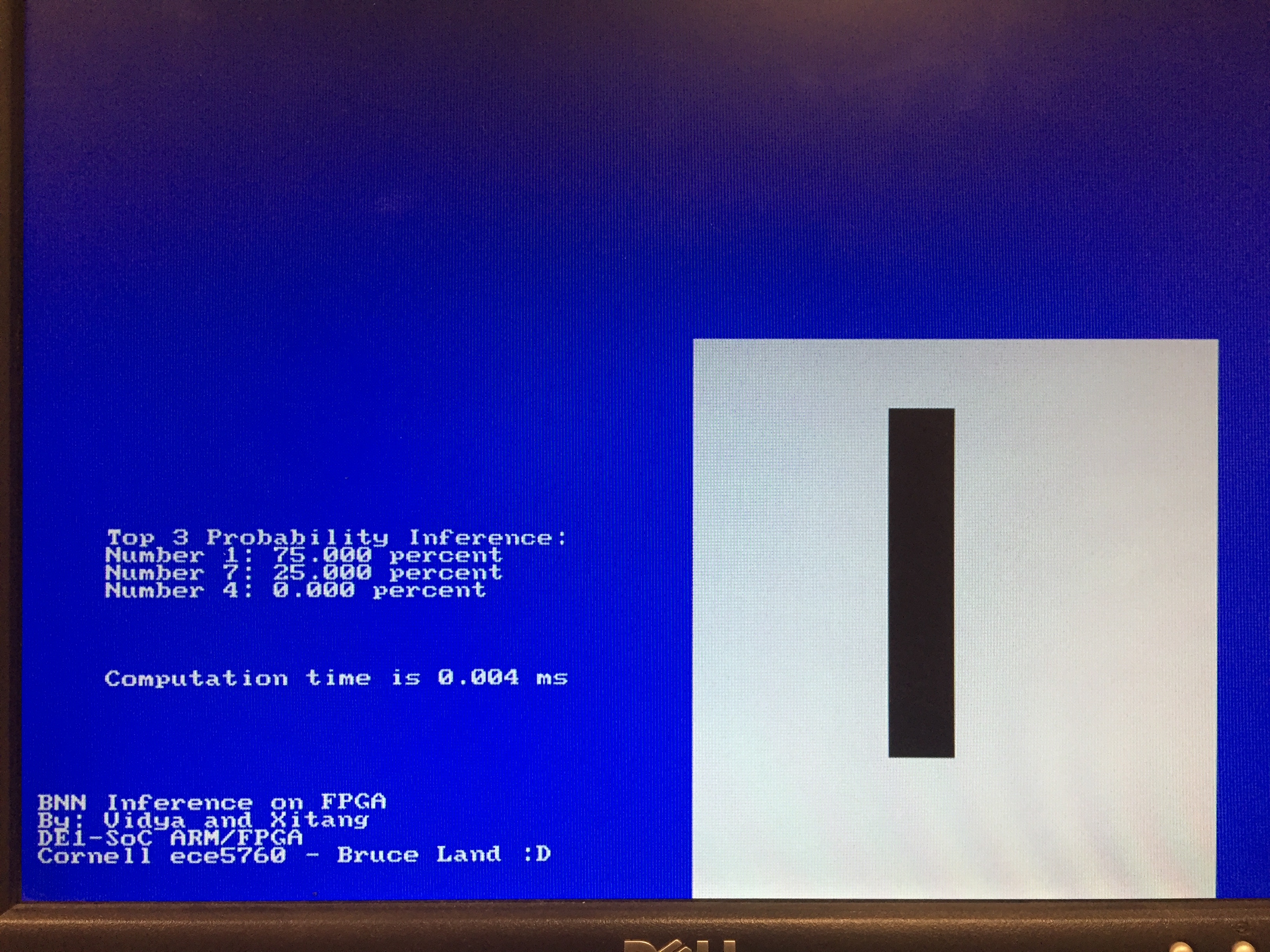
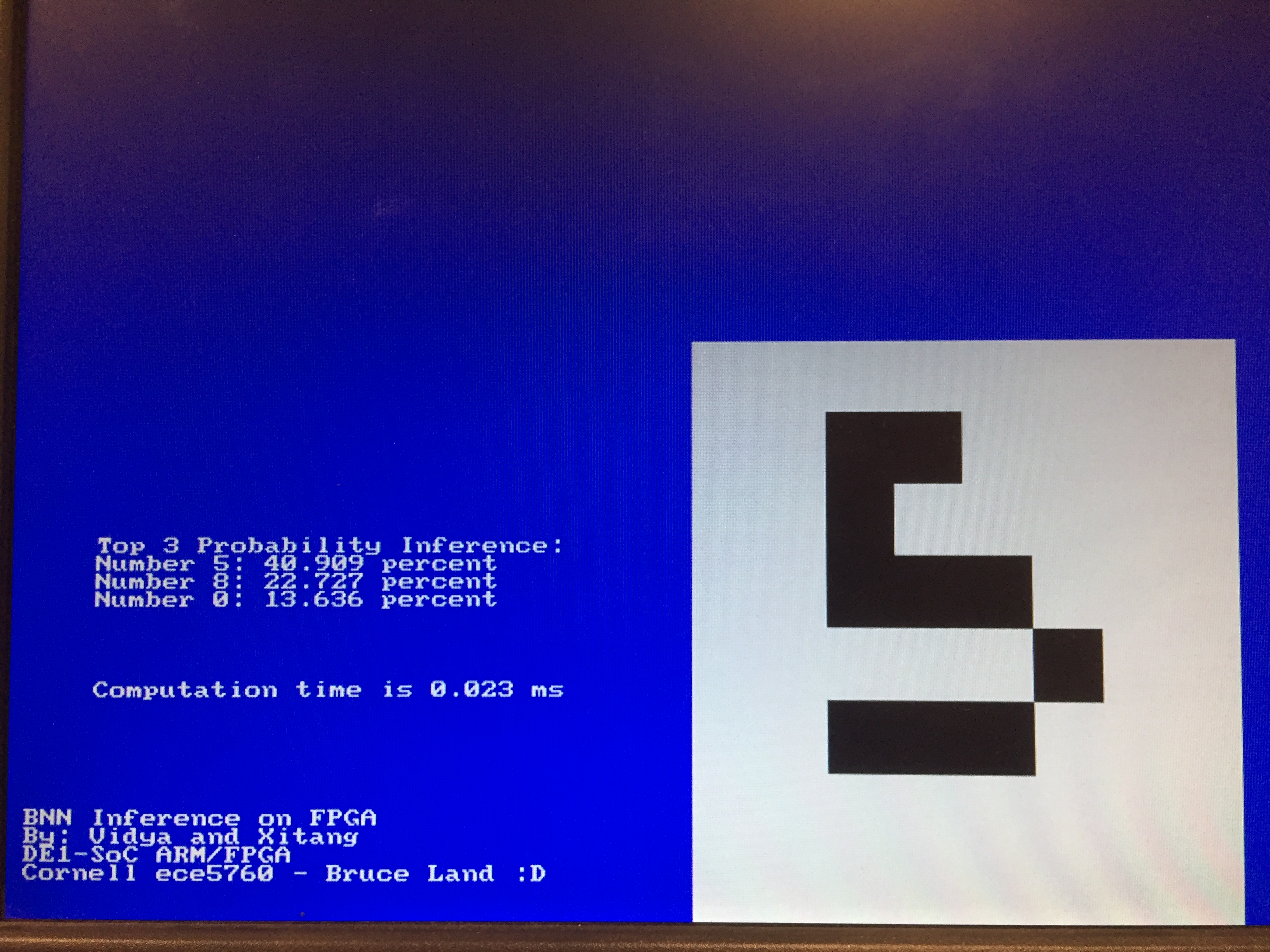
The speed of computation of the software model was measured by passing the finish signal indicating that the computation had finished back to the HPS and measuring the time between the start signal being sent from the HPS to the FPGA to the finish signal being sent from the FPGA back to the HPS. This FPGA BNN computation time was found to be around 0.004 ms or 4us. On the other hand, the Python implementation of the same BNN running on a PC takes about 44us. This time measurement is computed by the time duration it takes to run a Tensorflow Eval function on y_conv: y_conv.eval(feed_dict=test_dict), where y_conv is the last tensor layer of the BNN. In 1 batch size, we measures the time it takes to process 1 input, which is around 64.4ms and we also measures the time it takes to process 180 inputs, which is around 72.4ms. Because the processing time for a CNN is the total time of loading the weights and the computation, to extract a rough estimate of the time computing the weight, we use the time difference and (72.4ms-64.4ms)/180 data = 44us/data. Note that we were running the python code on a quad core PC. There are instabilities to measure time difference and various factors that can cause changes in the time measurement under a PC
Resource Usage
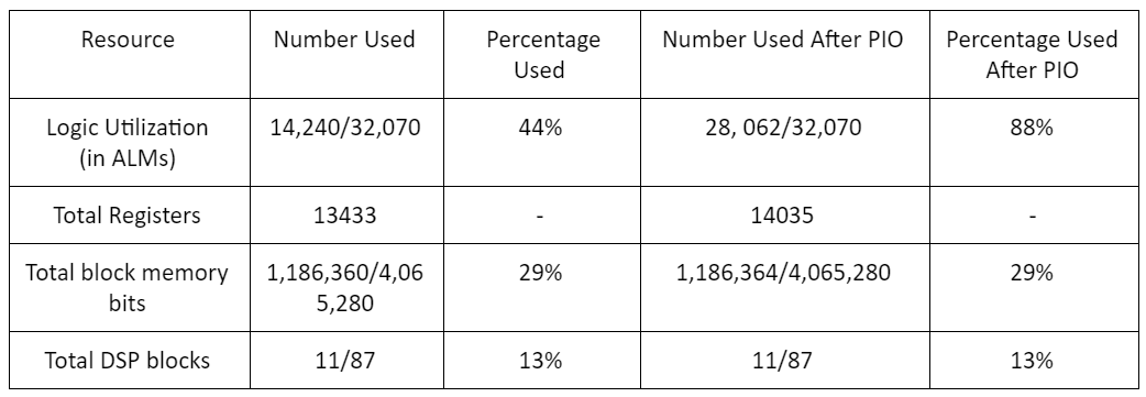
The table below summarizes some of the different resources used by the final implementation of our design. As can be seen, the BNN uses only a small fraction of the total memory available on the FPGA, and the use of ternary operators minimizes the need for multipliers/DSP blocks. The most used resource are the ALMs, but more than half of these are also still available on the board when the PIO ports used to transfer the output data to the HPS, communicate the start and finish signals in the design, etc. are not included. These results confirm the low resource requirements of BNNs.
Usability
The current design is not extremely flexible as input images must be hardcoded into the Verilog code in order to be processed. Since the weights are also hardcoded, any changes to these would also require the code to be modified and recompiled. The design could be made more configurable by using PIO ports or SRAM memory to transfer the weights to the FPGA from the HPS; however, with our current implementation the introduction of either of these elements results in the design not fitting on the FPGA. While digit classification is not inherently an extremely widely applicable task, image classification has many uses today. The speedup of the hardware classifier makes it more suitable for real time classification tasks in which timing is a major constraint.
Conlusion
For the most part, our implementation met our expectations. We initially had hoped for higher accuracy levels; we did not notice a bug in the Python implementation until much later in the development process. Correcting this bug was essential to making the Python design truly binary, but also led to around a 0.4 drop in accuracy (from around 0.8 to 0.4). Changes to the hardware of the net could accomodate for the changes needed to boost accuracy, but implementing those changes would take time beyond our deadline. As such, we chose to continued with our implementation of the lower accuracy model.
A feature we had hoped to include in our model was a camera interface which would allow images to be captured, pooled, and fed to the BNN in real time. While we had both the Verilog and HPS code needed to implement such a system, incorporating this feature into the design caused the total required ALM count to exceed that which was available on the board- prior to adding these changes our design used approximately 28,000 ALMs, after adding them the count jumped to around 38,000.
Intellectual Property Considerations
The net implemented was based on a framework implemented by a PhD student, Ritchie Zhao. The code provided was also based partially on a class assignment for a upper level course at Cornell. While there were no patent or trademark issues there are also no patent opportunities as the software design our hardware is based on is not of our own design. Our FPGA code was built using some of the resources available on the ECE 5760 course webpage. For example, the code we used to interface with the VGA display came from an example program on the class website. We did not use any other code from public domains beyond referencing online resources for relevant syntax and operations. There are no legal considerations which arise from our design that we are aware of.
Improvements and Future Work
If we were to do this project over, things we would change could include modifying the design of the net so as to support binary weights and non binary output feature maps from each layer, as this could improve accuracy. However, while our current implementation uses very few registers, a significant percentage of the ALMs available are being used, so such an implementation may not be feasible. Another potential change could be varying the size of the net. Currently, there are 16 output feature maps from the first convolutional layer, and 32 from the second convolutional layer and first fully connected layer. These numbers can be decreased to 8, 16, and 16 respectively. While this could result in a drop in accuracy, the smaller size could enable the design to fit on the board without using as high a percentage of the available resources, and could have allowed for additional features such as the camera and real time image classification.
Further improvements to the model could include extending the classification to process images from different datasets, such as the CIFAR10, instead of just digits. The neural nets used to process such images are more complex and typically require more memory and computational resources than those like the one we implemented. As we were already pushing the limits of the FPGAs computational resources with this net, we would likely need to use a larger board to implement anything more complex.
Acknowledgments
We’d like to thank Prof. Zhiru Zhang and PhD Candidate Ritchie Zhao for sharing Tensorflow Python code with us and for helping us navigate this project - it would have been significantly more challenging without their assistance. We’d also like to thank Prof. Bruce Land, who is always available to help us out in lab and provide guidance and support throughout the semester.
Appendix A
This group approves the video for inclusion on the course youtube channel.The group approves this report for inclusion on the course website.