ECE5760 Final Project: Vector Laser Projector
Reuben Rappaport (rbr76) | Emmett Milliken (eam348)
In this lab we used an FPGA to project vector image files using a laser and a set of motor-controlled mirrors known as galvanometers ("galvos"). Accomplishing this required us to move the galvos fast enough that the path traced out by the laser appeared to generate an image to a human observer. The FPGA with its immense signal processing and I/O capabilities was well suited for this high speed control task.
Although controlling the galvos is a good task for an FPGA, reading a vector image file from memory and parsing it into a form that can be easily drawn is a complicated sequential problem which is better accomplished on a microcontroller. In addition to the FPGA, the system on chip board we used also included an ARM based microcontroller known as the HPS or Hard Processor System. We ran an embedded linux distro on this system, providing us with a clean operating system environment to run code from. Using this HPS we were able to include a C component which does all of the preprocessing work and then forwards the path on to the FPGA to draw.
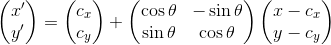
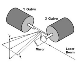
A galvanometer is a device which rotates to a specific position based on the applied voltage. We used two galvos with attached mirrors to control the path of a laser beam. Consider Figure 1 which shows the operation of a set of galvos. The setup consists of two mirrors held at a right angle along the y axis with their rotations around the x (for the y galvo) and z (for the x galvo) axes controlled by attached galvos. The laser first bounces off the x galvo and then the y galvo before exiting the device. The rotation of the x galvo controls the x position of the laser’s projected position and the rotation of the y galvo similarly controls the y position. By using the attached motors to adjust the mirrors, a controller can move the laser beam’s projection around at high speed.
Figure 1: Operation of a set of galvo motors[1]
Consider Figure 2, which shows the overall structure of our system. In order to draw a vector image file using our galvos we first passed it through C code running on the HPS which reads the file from memory, parses it, and passes it along to the FPGA. The FPGA then interpolates a sequence of positions along the vector path and uses a pair of DACs to send these positions to the galvos as analog signals. It also uses a general purpose I/O pin to send the digital on/off signal to the laser. These signals pass through electrical driver circuits which run the motors and laser. Finally, the physical system responds to the electrical signals by drawing the image with the laser
Figure 2: System diagram
The SVG (Scalable Vector Graphics) specification describes an efficient file format for encoding vector graphics files. In order to be able to display the many existing vector images created in this format, we chose to use the SVG standard as the basis for our project.
The SVG format is based on the structure of XML (eXtensible Markup Language). That is, SVG files consist of a tree data structure where each node begins with a <nodeName> tag and ends with a </nodeName> tag. Nodes enclosed between a node’s opening and closing tags are its children. Nodes may also carry attributes encoded in the form <nodeName attributeName=”attributeValue”>. The SVG standard describes a specific set of XML tags that can be used in this tree data structure and their meanings.
Although the SVG standard is quite large, the relevant piece of it for our project is the <path> element. This is the element used to describe the actual vector path itself. The path data is encoded as a string listing commands in a similar style to G-code. Each command consists of a letter to identify it followed by the numeric values it needs. This string is stored as the path element’s d attribute. Table 1 shows the available commands and their encodings.
|
Command |
Letter (Absolute) |
Letter (Relative) |
Data |
|
Move To |
M |
m |
X, Y |
|
Line To |
L |
l |
X, Y |
|
Vertical Line To |
V |
v |
Y |
|
Horizontal Line To |
H |
h |
X |
|
Cubic Bezier Curve To |
C |
c |
X1, Y1, X2, Y2, X, Y |
|
Smooth Cubic Bezier Curve To |
S |
s |
X2, Y2, X, Y |
|
Quadratic Bezier Curve To |
Q |
q |
X1, Y1, X, Y |
|
Smooth Quadratic Bezier Curve To |
T |
t |
X, Y |
|
Elliptical Arc To |
A |
a |
RX, RY, X-Axis-Rotation, Large-Arc-Flag, Sweep-Flag, X, Y |
|
Close Path |
Z |
z |
|
Table 1: SVG Path Commands
Paths always start with an absolute move to position all future coordinates. From there the commands define a sequence of path segments which can be lines, quadratic curves, cubic curves, or elliptical curves. The specification also includes shorthand forms for commonly used segment types - horizontal lines, vertical lines, and smooth bezier curves (which automatically infer their first control point). The close path command generates a line back to the start of the subpath.
Since SVG files are based on the extremely common XML format there are a number of open source libraries to read them from memory and parse them into a tree data structure. We chose to use the libxml2 library for this due to its clean interface, permissive MIT license, and general reputation for reliability.
After parsing the SVG files with libxml2, our next task was to extract the information we needed and discard the rest. We first pulled out the width and height from the root node’s attributes. Then we walked the tree looking for any path elements so we could extract their path data.
Unfortunately, since SVG paths are just encoded as strings, after we pulled the path data from the file we still needed to pass it through another parser to transform it into a useable form. In order to accomplish this we wrote a small parser using the flex lexer generator and the bison parser generator. This parser scanned the path string and spit out a linked list of segment commands. After parsing all the paths in the file we concatenated these lists together to create a single large path.
Before sending this path off to the FPGA we put it through several passes of preprocessing which helped to reduce the complexity of our FPGA code. We applied the following transformations
The scaling and offsetting transformation was a concession to the realities of our hardware. We used an 8 bit DAC to output the analog signal for each axis and therefore we only had 255 positions for each. Moreover, due to the difficulties of mirror alignment, we were reluctant to go all the way to the furthest positions of the galvos. Therefore we chose to shave off a 20 position barrier on either end of the scale. This resulted in transforming to the range [20,235]
Since it is possible to transform an elliptical arc into an equivalent series of cubic bezier curves with very little error, we decided to avoid implementing elliptical arcs on the FPGA and handle them in software instead. However, we ran out of time at the end of the project and never got around to actually implementing this functionality.
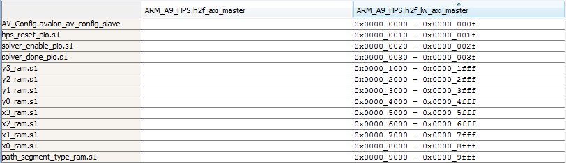
QSys is a proprietary Altera interconnect which handles the infrastructure to allow the HPS to communicate with the FPGA. Tools to place modules on the bus and assign them addresses are built into the Altera development environment. In order to talk to the FPGA from our C code we used the lightweight master on the QSys Bus. We first memory mapped the physical base address for the master into our C code’s virtual address space. We then added the appropriate address offsets for each component on the QSys bus in order to compute pointers we could use to talk to them. Figure 3 shows the address map for the QSys bus.
Figure 3: QSys Address map
In order to control the solver on the FPGA we used parallel ports to give the HPS access to both a reset line and an enable line. Holding the reset line high reset the system completely, while holding the enable line low caused the FPGA to finish drawing the image and then stop rather than repeating the image indefinitely. We used another parallel port running from the FPGA to the HPS to signal to our C code when the FPGA had reached this end state.
This enable/done interface allowed us to cleanly finish drawing an image before loading up a new one. Since all image paths begin and end at the center position, this resulted in no discontinuous jumps in the galvo position, smoothing their travel path. As the galvos are fragile and do not respond well to spikes or jumps, this was a desirable property.
In addition to the parallel port interface, we used an array of RAM blocks to hold the path data. These consisted of a path_type RAM block, which held an encoding for the segment type, and a set of X0, X1, X2, X3, Y0, Y1, Y2, Y3 RAM blocks, which held the control points for each segment. The nth entry in a given block corresponded to the nth entry in all of the others. Since not all command types used all four control points, we just left the unused entries blank. We also included a special END command as the final entry in the RAM block, signalling to the state machine that it should go back to the beginning and repeat the image path.
Making the projected image rotate is a complicated transformation involving sines and cosines. Since this rotation runs on a much slower timescale than the high speed analog signals used to control the galvos, we chose to do the math on the HPS and periodically send over a new frame to the FPGA. We found that a slow rotation speed (> 3 seconds per rotation) combined with an update rate of 10 frames per second created relatively smooth motion.
We chose to do all of our math in signed two's complement 10.18 fixed point format. Since our output needed to be an unsigned 8 bit number, the choice of 10 integer bits allowed us to conveniently detect both overflow (the second highest bit is set) and underflow (both of the top two bits are set). The 18 fractional bits allowed us to interpolate along the path with high precision.
While younger than many purely mathematical fields which go back centuries or even millenia, Computer Graphics has today been a field of interest for over 60 years. This means that nearly all straightforward graphical tasks have classic and well-established algorithms to perform them. Among these is Bresenham’s Line Algorithm which provides an elegant approach for drawing a line between two points on a pixel grid.
Bresenham’s Line Algorithm separates this task into two cases - one where the magnitude of the line’s slope is less than or equal to one, and another where the magnitude of the slope is greater than or equal to one. We’ll start by considering the first case.
|
plotLineLow(x0,y0, x1,y1) |
Listing 1: Bresenham’s Line Algorithm for slopes less than or equal to one[2]
Consider Listing 1, which shows the pseudocode for this algorithm. On each iteration through the loop we increment x and update D. Whenever D exceeds 0 we also increment y. This allows us to step along the line pixel by pixel.
|
plotLineHigh(x0,y0, x1,y1) |
Listing 2: Bresenham’s Line Algorithm for slopes greater than or equal to one[3]
Now consider Listing 2, which shows the pseudocode for slopes greater than one. This algorithm is totally symmetric to the first case: we increment y on every iteration and increment x when D exceeds 0. Using Bresenham’s algorithm merely requires deciding which case to apply and then delegating to the relevant subroutine.
To allow us to interpolate points for line and move svg path commands, we built an implementation of Bresenham’s Line Algorithm in hardware on the FPGA. We designed modules implementing both lineLow and lineHigh and then wrapped them in a higher level module which muxed the two together so that the appropriate one is sent to the output.
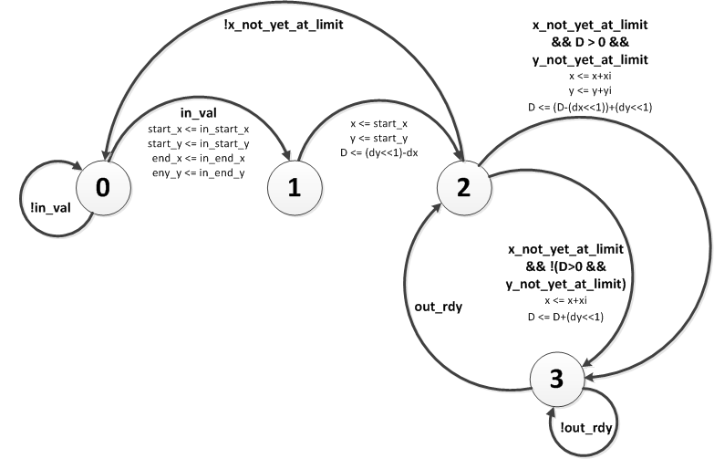
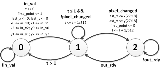
Figure 4: State machine diagram for lineLow module
Figure 4 shows the state machine for the lineLow module. The system is initially in state 0 waiting for valid input. When the in_val line goes high, it transitions to state 1 and copies all of the values from the input wires into registers. On the next cycle it initializes x, y, and D and transitions to state 2 where it begins running the loop. On each pass through the loop it increments x, updates D, and increments y if D > 0. It then transitions to state 3 where it raises out_val and waits for the out_rdy line to go high, indicating that the other side is ready to accept the transaction. When this occurs it goes back to state 2 and computes the next point. When x finally reaches the end, it transitions back to state 0 and raises done, signalling the top level module that it has completed the line. It then waits for in_val to go high again, at which point it begins computing the new line.
The implementation for lineHigh is completely symmetric with the roles of x and y exchanged.
In order to protect the output from over and underflow, the wrapping module checks the top two bits of x and y. If the top bit is set, indicating underflow, then it returns 0 instead. If the second highest bit but not the top bit is set, indicating overflow, then it returns 255 instead. This prevents overflow errors from propagating to the output.
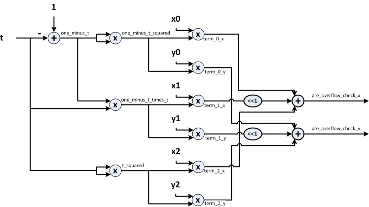
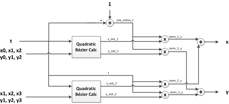
Unlike lines, which have a simple pixel interpolation algorithm that does not require multiplication, implementing the equivalent of Bresenham’s line algorithm for quadratic curves is quite complex. We therefore decided to interpolate along the simple parametrization of a quadratic Bézier curve in terms of its control points.
Figure 5 shows the block diagram for the circuit implementing this equation. We first compute the  ,
,  , and
, and  . We then multiply each of these terms with both the
  and
and  inputs for each control point and sum them together to create
the and outputs. The multiply by two for the second term is implemented using a left shift. Before sending our results to output we pass
them through the same overflow protection circuit we used for the line. This design results in a two multiply output latency for the circuit.
inputs for each control point and sum them together to create
the and outputs. The multiply by two for the second term is implemented using a left shift. Before sending our results to output we pass
them through the same overflow protection circuit we used for the line. This design results in a two multiply output latency for the circuit.
Figure 5: Quadratic Bézier curve block diagram
Interpolating along the parametric equation like this creates a few problems. Depending on our step size for  , we may skip over some pixels and create discontinuous jumps in
the galvo position. Alternatively, some pixels in the output image could have more interpolated points alias to them than others. Due to the nature of our physical setup, this will result in the laser spending more time at those pixels and
therefore those positions appearing brighter than their neighbors.
, we may skip over some pixels and create discontinuous jumps in
the galvo position. Alternatively, some pixels in the output image could have more interpolated points alias to them than others. Due to the nature of our physical setup, this will result in the laser spending more time at those pixels and
therefore those positions appearing brighter than their neighbors.
We deal with the first problem by choosing a small step size (we chose 1/512, which is more than enough for our 255 x 255 output grid). In order to deal with the second we built logic into our state machine to only output points when the pixel they alias to changes. This results in it taking a variable and possibly large number of cycles to compute the next point in the curve. However, since our solver is running on a much faster clock than the clock used to feed output to the galvos, this irregular rate of production causes no problems and we always have points ready when we need them.
Figure 6: State machine for quadratic Bézier interpolation module
Figure 6 shows the state machine for our quadratic Bézier interpolation module. We use the same interface as the line module to make communication uniform. Initially we are in state 0 waiting for valid input. When
in_val goes high we copy our inputs to our registers and transition to state 1. In state 1 we increment . We compare the output of our interpolation circuit to
last_x, and last_y which store the value of the last pixel we sent to output to determine if the pixel has changed. If the pixel has changed, or if it’s the very
first point then we advance to state 2, raise out_val, and wait for the top level module to accept our output by raising out_rdy. When this happens we complete the
transaction and return to state 1 to continue interpolating. If the pixel has not changed then we remain in state 1. When finally reaches 1 we return to state 0 and raise done, telling the top level module that we have completed the curve.
Like quadratic Bézier curves, cubic Bézier curves do not have a simple Bresenham style pixel interpolation algorithm. Therefore we again chose to implement them by stepping from 0 to 1 in their parameterized form.
Whereas the parametrized form of a quadratic Bézier curve is a weighted sum of lines, the parameterized form of a cubic Bézier curve is a weighted sum of quadratic Bézier curves. This conveniently allows us to reuse the calculation code from our quadratic Bézier interpolation model.
Figure 7: Cubic Bézier curve block diagram
Figure 7 shows the block diagram for the logic implementing cubic interpolation. We take the and outputs of the two
quadratic Bézier curves and multiply each of them by the appropriate weight before summing them to create the output. This adds an additional multiply to the sequence, creating a three multiply latency for the overall circuit.
The cubic Bézier interpolation module uses the same interface and has the same state machine as the quadratic Bézier interpolation module. The only difference is that it uses a more complex circuit to interpolate
new values for and .
After creating modules to interpolate pixels along the three different path segment types, we created a top level solver module to read commands from RAM and dispatch them to the appropriate interpolator. We created 9 separate RAM blocks - one for the segment type, and eight to hold the x and y coordinates of the four control points. The nth entry in each RAM corresponded to the nth entry in every other RAM meaning that commands which did not need all four control points just left holes in some of the RAMS.
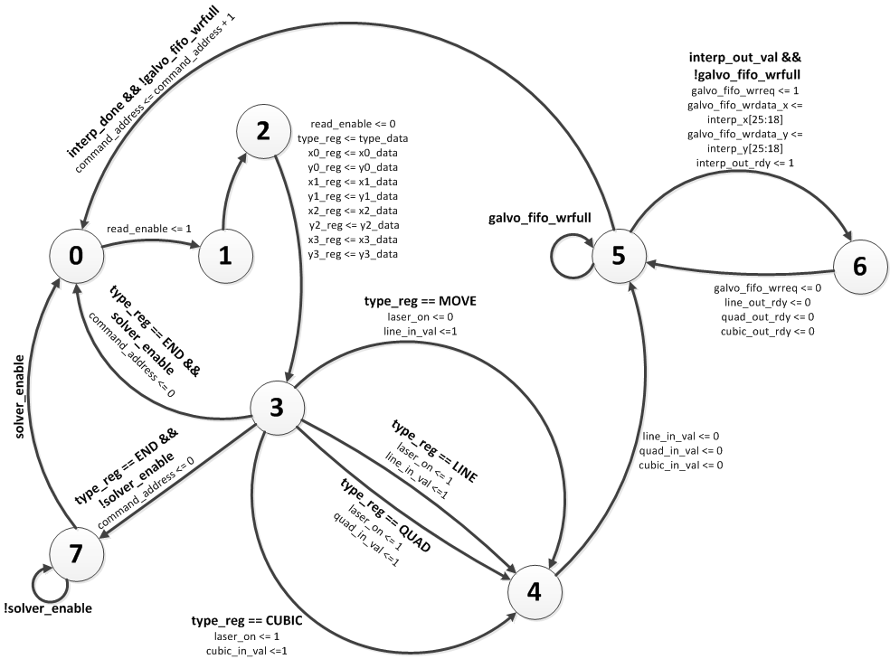
Figure 8: Top level SVG solver state machine diagram
Figure 8 shows the state machine for the top level solver. We begin in state 0 where we issue a read to the nine RAM blocks in parallel. We advance to state 1 and then to state 2, at which point the result of the read is ready, and we transfer the outputs of the RAMs into our registers and continue on to state 3. We then dispatch a command based on the contents of the type register. If it’s a move command we turn the laser off and send the control points to the line module, whereas for a line command we use the line module but keep the laser on. For quadratic Bézier curves we use the quadratic curve module and for cubic Bézier curves we use the cubic curve module. In both cases the laser remains on. For all of these commands we advance on to state 4. If instead the type register holds the special END command then we have reached the end of the path. If the solver is enabled then we reset the read address to 0 and return to state 0 to start the path from the beginning again. If not then we move to state 7, raise the done parallel port, and wait for the solver to be enabled again so we can return to state 0.
In state 4 we lower in the in_val lines and move on to state 5 where we wait for there to be space in the output fifo and for either the out_val or the done line of the relevant interpolator to be raised. If done is raised then we increment the read address and return to state 0 to read the next command out of the RAM. On the other hand, if out_val is raised then we raise out_rdy to complete the transaction, write the point and the laser’s status to the output fifos, and move on to state 6. Finally, in state 6 we finish the fifo write and return to state 5 to wait for the next point or the completion of the segment.
The cheap galvos we used are incapable of responding accurately to control signals at the high speed our solver runs at. In order to deal with this mismatch between the rate we consume points and the rate we produce them, we used a set of fifo queues - one for the x channel, one for the y channel, and one for the status of the laser. The write side of these queues is on the solver clock, and the solver only produces points when there’s enough space in the fifos to store them. The read side of the queues is on the much slower clock, which drives the galvos.
In order to generate this read clock, we used a counter incremented on the rising edge of our 50 MHz reference clock as a clock divider. We then muxed together several different high order bits of this counter and used some of the board’s switches as the select line. This gave us the ability to control the speed of the galvo clock by flipping a few switches.
The x and y data read from the fifos was then sent to the high-speed 8-bit DACs on the board. This hardware was originally intended to be used for the analog color channels on the VGA port, but by disabling the regular VGA functionality we were able to repurpose them as drivers for our galvos. We put out the laser’s control signal on a general purpose I/O pin, as it is controlled by a digital signal rather than an analog one.
Although there are some nonlinear projection effects which we could compensate for by passing the output through an arctangent function, at the angles our system deals with small angle approximation makes them too small to be relevant.
For this project, we used a deconstructed, cheap laser pointer purchased off Amazon. Instead of the AA batteries it was designed for, we used a small, 5V DC power supply we had lying around.
We needed to turn the laser on or off depending on what type of command was being executed. In order to render the image correctly, the laser needed to be off during move and end commands and on during line, quadratic curve,and cubic curve commands.To accomplish this, we used one of the FPGA’s GPIO pins to output the laser_on signal generated by the solver.
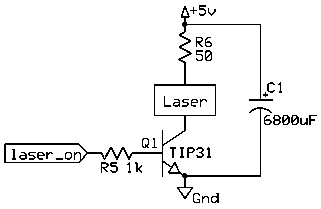
Figure 9 shows our laser driver circuit. We used a TIP31 NPN transistor driven at the base by laser_on to form a low side switch. We limited the current drawn from the I/O pin using a 1kΩ resistor, R5, so as not to damage the FPGA pin and we limited laser current using a 50Ω resistor, R6, to prevent overheating and bring down the brightness of the laser to a comfortable level. After some testing we added capacitor C1 to reduce the voltage ripple caused by the laser circuit as it was causing distortion in the galvanometer amplifier circuit.
Figure 9: Laser driver circuit.
We ultimately ended up ordering the cheapest galvanometer setup that we could find, which was from Seeed Studio[4]. However, with the low price came very little in the way of clear documentation. When we received our order it contained the assembly with the two galvanometers, a driver board, and a power supply. After some puzzling over the documentation and cables we determined how to hook them all together properly.
The provided power supply output +15V, ground, and -15V, which were all fed to the driver board. The driver board then took two analog control signals in the range of -12V to +12V to control the angles of the X and Y galvos. In order to move the galvos fast enough to generate a recognizable image, we needed high speed digital to analog converters (DACs). Luckily our FPGA board came with a set of high speed 8-bit DACs meant to be used by the VGA module which we commandeered for this purpose.
While the VGA DACs were fast enough to control the galvos, the output voltage range was 0V to 0.7V so we needed to offset and scale the VGA outputs before sending them to the galvo driver circuit. We accomplished this using two differential op amps.
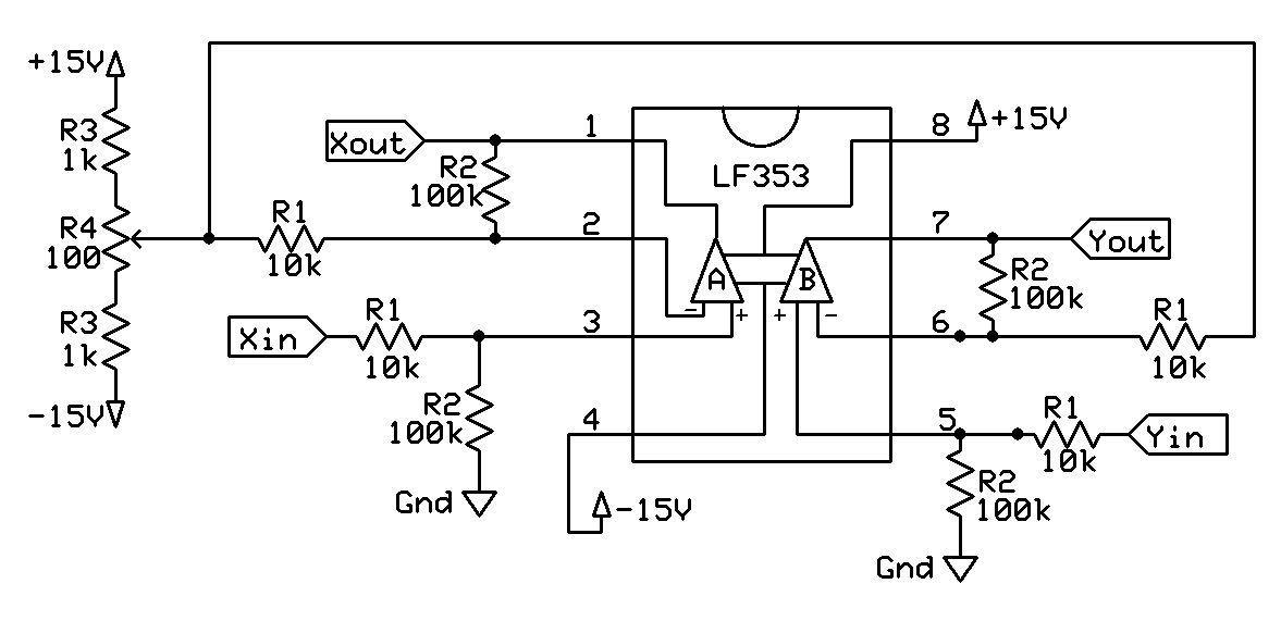
Consider Figure 10 which shows our galvo driver circuit. A differential amplifier amplifies the difference between the two inputs. The inverting input of the op amps was a DC voltage, therefore the output was the non-inverting input signal offset by the DC voltage and then amplified. The voltage divider on the left formed by potentiometer R4 and both R3 resistors was used to adjust the offset voltage. The gain of the amplifier was determined by the ratio of R2 to R1. We chose R1 and R2 to achieve a gain of 10, as it kept the galvo inputs safely within the center of the range.
Figure 10: Amplifier circuit used to convert the VGA DAC X and Y outputs (0V to +0.7V) to the input range of the galvanometers (-12V to +12V).
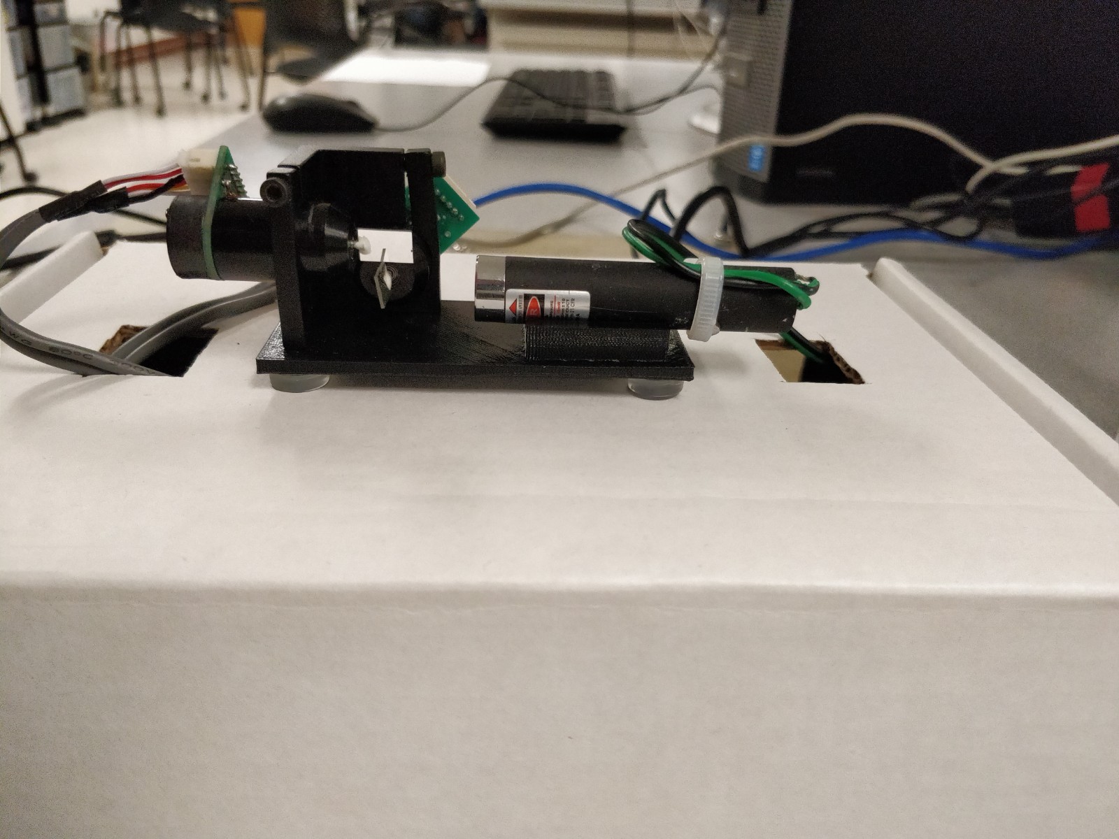
In order to mechanically align the laser with the galvo mirrors, we designed and 3D printed a small mounting part. We screwed the galvos down onto the mount and used an aligning tab for the laser to glue it in the correct place. Finally, we added stick on feet to the bottom of the mount so it could stand level. Appendix E provides a link to download the CAD file. Figure 11 shows the mechanical setup.
Figure 11: Mechanical alignment of laser and galvos
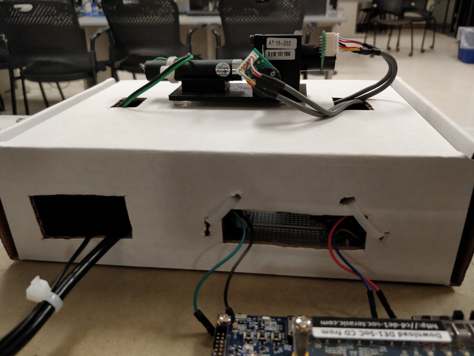
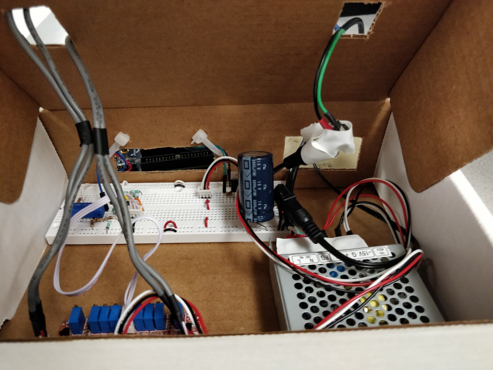
We placed the circuitry inside a sturdy cardboard box, put the mounted galvos and laser on top, and cut holes in the box to allow cables to enter and leave where appropriate. Figure 12 provides a back view of the enclosure and Figure 13 shows the contents.
Figure 12: Back view of enclosure
Figure 13: Interior of enclosure
Before doing any work in Verilog, our very first step was to make sure that we could drive the galvos we had ordered. We set up the VGA DACs to output a sine wave on the y channel, and a cosine wave on the x channel using direct digital synthesis, and we built our amplifier circuit. After verifying that the DAC output was correct, and then that the amplified DAC output was correct, we hooked our system up to the galvo driver board and shined the laser pointer at the mirrors. It was difficult to hold it steady, but we were still able to see a very clear circle in the output - a great first start.
Next, before we moved on to compiling FPGA code, we spent a period of time testing our solver design in simulation to make sure that it behaved correctly. We individually tested each of the different interpolator modules, and then we tested the top level solver module all together. In each case we exported the simulation’s output waveform and plotted it in MATLAB to verify that we were interpolating points along the path correctly.
After we managed to get the solver working on the FPGA, we hooked up oscilloscope probes to the DAC channels to look at the waveforms. When we were satisfied that they were right, we passed them through our amplifier circuit, and from there into the galvo driver board. At this point we managed to get the motors moving correctly, but for some reason our design was never turning the laser on. To diagnose this issue we recompiled our FPGA code with SignalTap - an Altera logic analyzer tool which allowed us to record waveforms in an onboard RAM, and view them over USB. Using SignalTap to debug our system, we were able to track down the issue and get the whole system working.
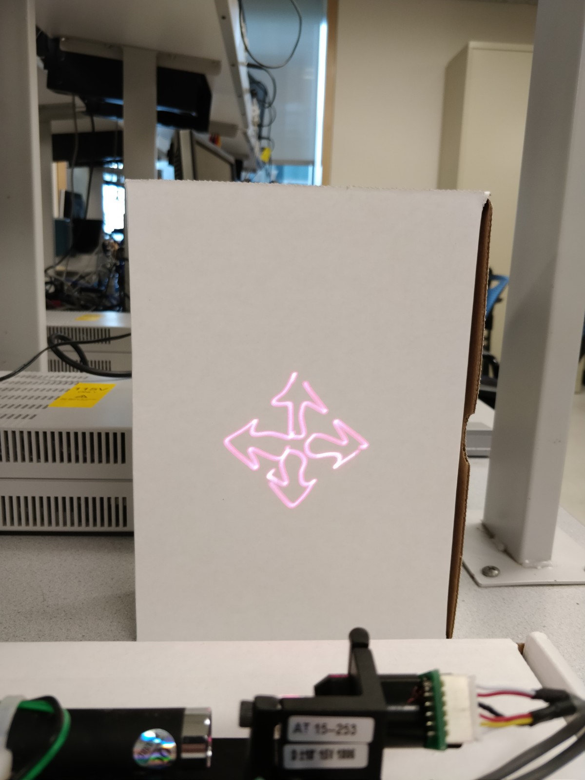
Once we had reasonable looking laser output, we did most of our testing by visually confirming the results. We tried projecting several different svg files - a set of four arrows, a single large arrow, a biohazard symbol, and a lightbulb. Based on the problems we encountered with these, we were able to diagnose design issues and make changes to improve the system. One major issue we faced is distortion of the analog signal going to the galvos. We were able to reduce, though not eliminate, the distortion by reducing the length of the hookup wires carrying the analog signal from the VGA, moving the laser circuit further away from our amplifier circuit, and adding a large capacitor over the power supply for the laser.
Figure 14: Example of laser projector output
Figure 15: The input file which produced Figure 14
Figure 14 shows an example of our laser projector’s output and Figure 15 shows the input file which produced it. Although it’s quite clear and coherent, the paths are distorted and what should be straight lines rendered as curves. Over the course of our experimentation we found that increasing the speed of the clock driving the galvos made the output much clearer and reduced flickering, but also made the distortion significantly worse. Moreover, we found that as we ran the system for longer and the galvo driver board began to heat up, the distortions became worse and worse. Part of this problem could have been alleviated by providing the galvo driver circuit with better ventilation, though a large part of the distortion seemed to be inherent to the hardware we were using.
We were happy with our results, although we of course wished that they could have been better. Overall, we accomplished what we set out to do, which was to create a working vector laser projector, as well as a SVG parser to go with it. The quality of our rendered images was not ideal, but it’s not clear that doing any better was possible with the cheap galvos we picked up. If we’d had a little more time to work on the project, we would have spent more time trying to improve the image quality. We also would have liked to have implemented support for elliptical arcs or to have added support for more types of SVG animation than just rotation. Given the limitations of the time span of the project and the budget, we count this as a win.
As far as intellectual property considerations go, we used several open source tools with permissive licenses to build the HPS part of the project. We used a linux kernel released under the GPL license, the libxml2 library released under the MIT license, the flex lexer generator released under the BSD license and the bison parser generator released under the GPL license. We also used some non-redistributable Altera IP to build our FPGA code.
All told, we had a good time with this project and we’re proud of the work we did. Thank you to Bruce and all of the TAs for the help!
The group approves this report for inclusion on the course website.
The group approves the video for inclusion on the course youtube channel.
|
Emmett Milliken |
Reuben Rappaport |
|
|
Table 2: Work Distribution Table