
Lorenz ODE Solver on DE1-SoC using Simulink Workflow
Built by Vipin Venugopal and Parth Bhatt
Project Demo
Introduction
The objective of this project is to explore an alternate approach for implementing systems on Intel-DE1-SoC. Intel and MathWorks have collaborated to deliver a suite of design tools aimed at providing seamless integration of system models developed in MATLAB* and Simulink* with Intel® FPGAs and SoCs.
Engineers using MATLAB and Simulink for system modeling, algorithm development, visualization, and advanced debugging can easily target Intel FPGAs. In addition, they can be guaranteed that the code generated will be optimized and ready for deployment and production.
The goal is to build the Lorenz first order differential solver on the Intel DE-1 SoC using MATLAB/Simulink software. The system is similar to the Lab1 of the ECE5760 course. In the lab1, this project was developed using Verilog HDL on Quartus Prime software and the Connections were done using QSys/ Platform Designer.
The project was carried out in 3 phases:
- Software Setup and Workflow Validation
- Design and Testing of Lorenz ODE Solver
- Extending the workflow to reuse QSys IP cores
Phase 1: Software Setup and Workflow Validation
Software Setup
In order to build the FPGA project on Simulink, the system requires various software applications and support packages with appropriate versions. The software are listed below:
- MATLAB version 2018 or above
- HDL Coder Support Package for SoC (Latest Version)
- Embedded Coder Support Package for SoC (Latest Version)
- Intel Quartus Prime V17.0 (licensed version)
- Intel SoC Embedded Design Suite
Note: The system needs a restart after the installation of all the above-mentioned software.
Hardware Setup
The hardware required for this project was Terasic DE1-SoC development board, Power Supply Adapter, USB blast, USB serial cable, and Ethernet cable (the computer and the SoC board should be on the same network).
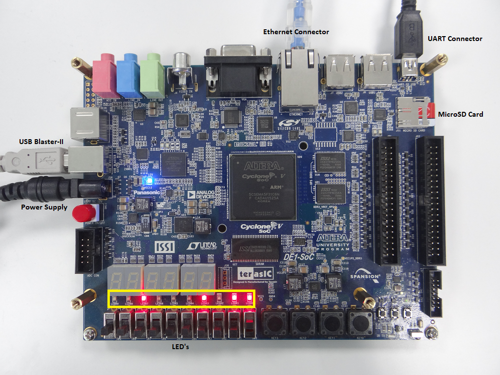
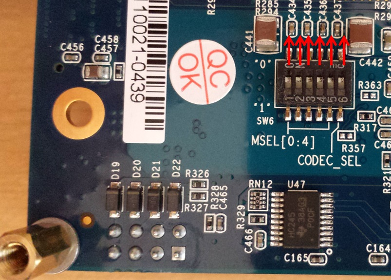
The switch configuration on the Terasic DE1-SoC board needs to be changed as shown in Fig. The switches are for selecting the programming source for the onboard FPGA and can be found at the bottom surface of the board.
Setting up the Linux Image
The Linux that was used in this project was the one provided on setup page provided by MATLAB. (Linux Image)
Thi Linux image can be uploaded into the SDcard with the help of Etcher software.
Setting up MATLAB
The following steps are to be followed in order to setup the MATLAB:
- In the MATLAB command window, enter the following command
hdlsetuptoolpath('ToolName', 'Altera Quartus II', 'ToolPath', 'C:\intelFPGA\17.0\quartus\bin64\quartus.exe');
This command is used to store the path for Quartus in the MATLAB
h = alterasoc('
The default IP address for the board is 192.168.0.101 and the default password is ‘cyclonevsoc’
addpath(fullfile(matlabroot,'toolbox','hdlcoder','hdlcoderdemos','customboards','DE1SOC'));
The settings for this board are already provided along with the HDL coder installation.
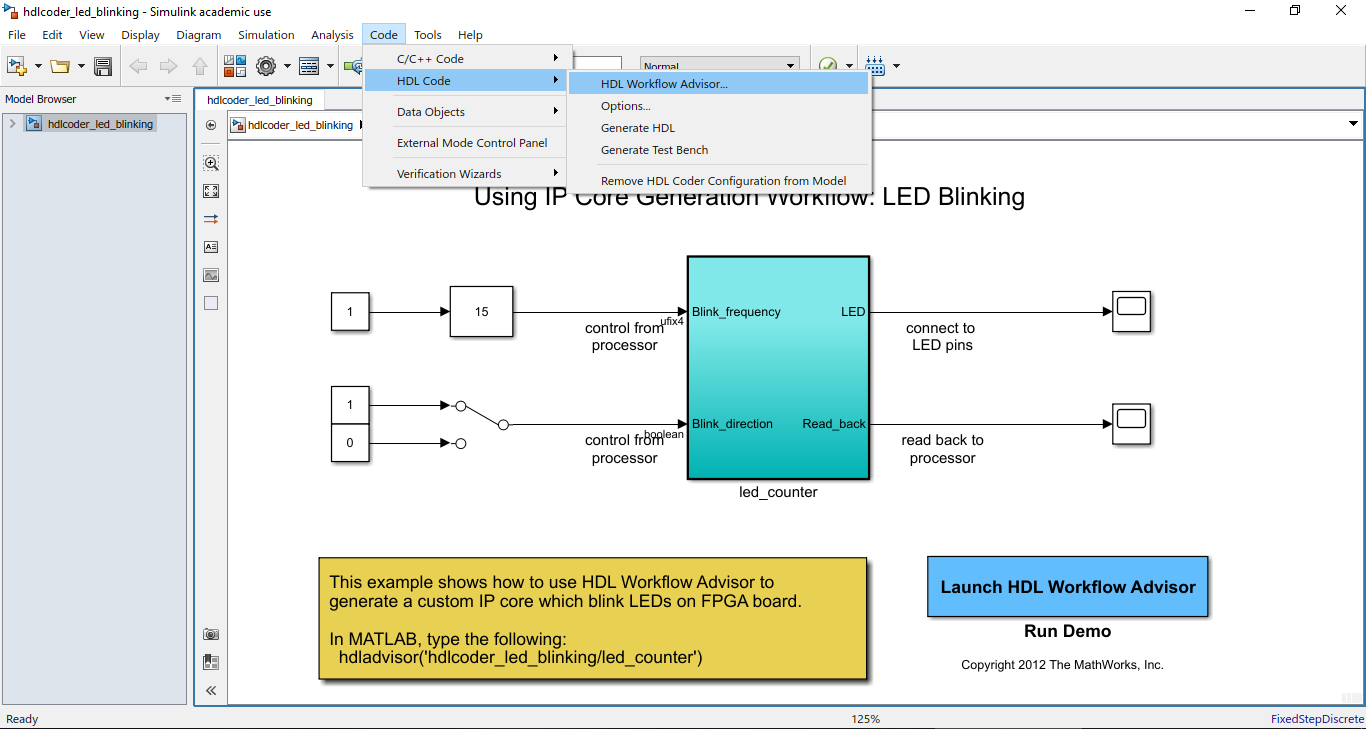
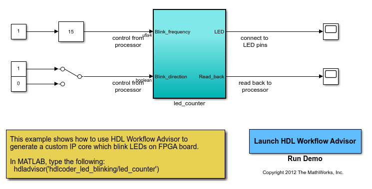
open_system('hdlcoder_led_blinking');
Workflow Validation
LED counter program:
Before starting with the Lorenz model, the setup needs to be tested with an already tried and tested example program. In order to do this, the example code previous opened in MATLAB setup is used. The command ‘open_system’ opens a window with a ‘led_counter’ subsystem. The following are the new steps to be executed:
- Select ‘Code>HDL Code>HDL Workflow Advisor’ as shown in the figure below.
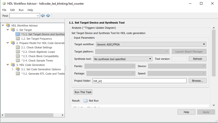
- Target workflow: IP core Generation
- Target Platform: Terasic DE1-SoC development Kit
- Synthesis Tool: Altera Quartus II
- Tool Version: 17.0.0
After the above settings are configured correctly, select “Run this Task” for steps 1.1 and 1.2. If the step 1.1 is configured correctly, then the software should display two extra steps in the first section.
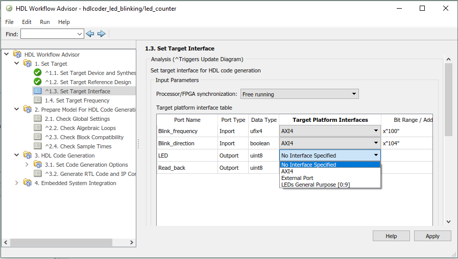
Here, Blink_frequency, Blink_direction and Read_back are set to AXI4 interface whereas LED is set to ‘LEDs General Purpose [0:9]’
Note: For task 4.3 to run correctly, Quartus needs to be registered with full license and configured currently with MATLAB.
Phase 2: Design and Testing of Lorenz ODE Solver
Design
The Lorenz system is a system of ordinary differential equations exhibiting chaotic behavior for certain parameter values and initial conditions. For this system, the benchmark used is a Lorenz ODE solver built using Verilog and Quartus workflow. The detailed description of the benchmark Lorenz ODE solver can be found on the web page for lab 1 of ECE5760 course at Cornell University.
The three equations in the part of Lorenz solver are:
dx/dt = sigma*(y-x)
dy/dt = x*(rho-z) - y
dz/dt = x*y - beta*z
The variable parameters in this equation are the initial conditions for x1, x2 and x3, values of the constants - sigma, rho and beta, and the time constant dt.
When the solutions for the 3 variables are plotted against each other in 3D, it resembles a butterfly.
The Simulink model that was developed for this purpose is given below. The figure shows the top layer of the Simulink model.
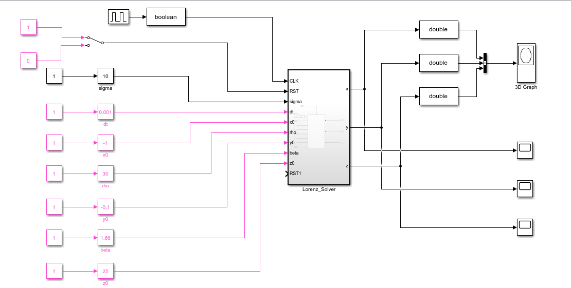
The Lorenz_Solver is the subsystem which will be synthesized and downloaded to the FPGA. The remaining blocks form part of the user interface and runs in Simulink. Simulink automatically sets up a software interface model to send these parameters and receive the feedback from FPGA over the AXI interface to the HPS and also the interface to transfer these values between HPS and Simulink over ethernet.
The Lorenz_Solver is configured as edge-triggered so that a new solution point is generated on every rising edge of trigger pulse. A clock module is used to generate triggering for the Lorenz_Solver. Adjusting the clock period allows us to speed up or slow down the solution. However, Simulink doesn’t allow the top layer to be a triggered subsystem. The simple solution for this was to have one more level of triggered subsystem inside the Lorenz_Solver subsystem.
A reset is provided to reset/start the solution at any point of time. On pressing this, the variables are reset to initial values. The other inputs to the system are
x0,y0,z0: initial values of the variables
sigma, beta, rho: parameters
dt: Step size for Euler integrator
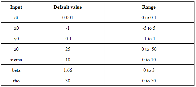
These values are varied using slider gain blocks in Simulink. These blocks allowing setting of range and default values for these inputs. The settings are shown in the table.
The outputs of the system are the values for the 3 variables x,y and z.
The outputs are visualised using 2 Simulink blocks. The scope allows plotting of each variable independently with respect to time and 3DScope allows plotting of the 3 variables with respect to each other in 3D.
The Lorenz solver block is given below.
The lorenz solver is implemented based on the Lorenz equations rearranged to avoid overflow:
x[t+dt] = x[t] + (dt*sigma) * (y[t]- x[t])
y[t+dt] = y[t] + (dt*x[t]) * (rho- z[t]) – (dt *y[t])
z[t+dt] = z[t] + ((dt*x[t]) * y[t]) –( (dt*beta)* z[t])
To create the models, the right hand side of the above equations were implemented in block level using adders and multipliers. The resultant equations were fed to an accumulator block. The outputs of the accumulator were fed to unit delay blocks. The delayed outputs are fed back as input to blocks to be used for calculations in the next cycle.
Based on the experience with benchmark system, 7.20 fixed point system was adopted for data, where 1 bit is signed, 6 bits represent decimal and 20 bits for the fraction. Due to this format, the multiplication needs to be done carefully. After the multiplication, the output obtained is in 54 bits format hence, the 1 signed bit, 6 integer part and the 20 bits of the fraction. The input data and output data type properties for each simulink block within the solver, can be set accordingly using GUI.
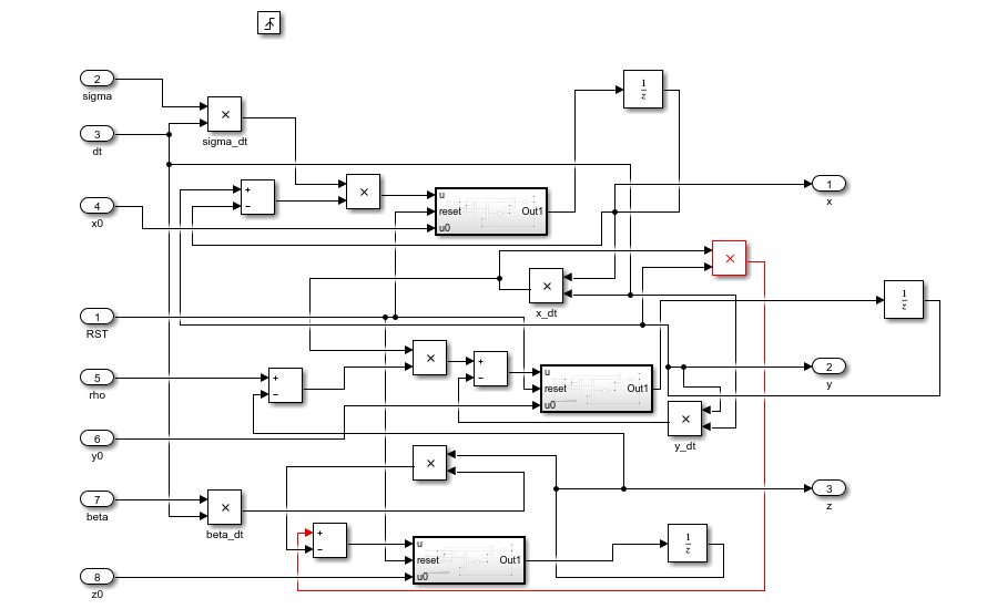
This is quite similar to the RTL model generated from benchmark Verilog design.
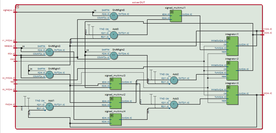
The accumulators used in the system are Euler integrators. Euler method determines the integral by accumulating the finite differences to the initial value. The built-in Euler integrators in Simulink does not support external inputs for initial values. Since the initial values of the variables had to be a user configurable value, euler integrator had to be built from basic modules.
Testing:
The first step was to verify the correctness of Simulink model. To do this the model was simulated in normal mode without HDL generation. The output waveforms were verified on time scope and 3D scope. The parameters were varied and the effect of variation was observed on the scopes.
The HDL workflow was then used following the same steps as LED Blinking to generate the code. The workflow is same as the LED blinking except for setting Target Interface.
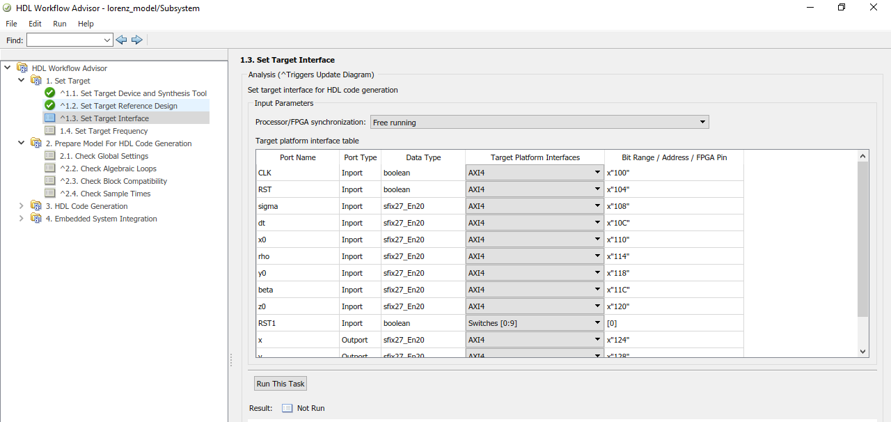
After the workflow is completed the following reports are generated.
Target platform interface table:
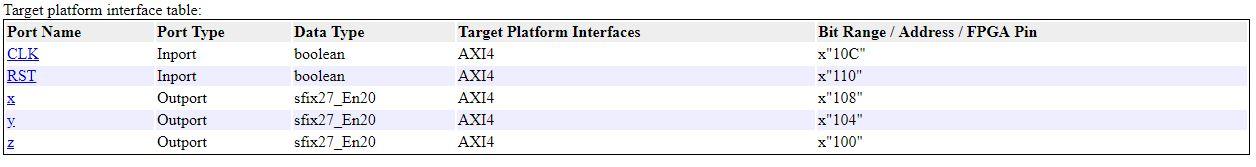
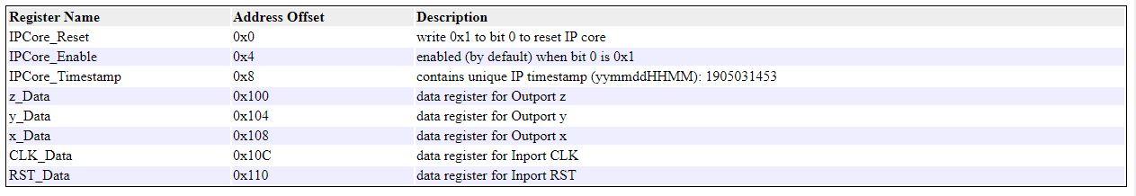
The following AXI4 bus accessible registers were generated for this IP core:
After programming the bitstream, the generated model was simulated in external mode to verify the operation. Initially, the output was not sensible as the solution was too fast to visualize. This was resolved by making the subsystem as triggered subsystem and using a slower user configurable clock to trigger the system. The Simulink model was re-simulated in normal mode. But this led to errors, as the output of the solver was directly fed back to input leading to loops. This is not permitted in triggered systems. To overcome this, a unit delay was added to the output before feedback. The Simulink model was then successfully simulated and tested in normal mode. The new model was used to generate the HDL implementation using the HDL code workflow. The newly generated system successfully ran on the FPGA and the effect of varying parameters was observed on the scopes.
The slider Gain switches were replaced by knob model is Simulink to make the User interface more intuitive. The three single scopes were also replaced with a single 3 input scope.
Phase 3: Extending the workflow to reuse QSys IP cores
The Lorenz ODE solver implemented in the previous section generates an IP core integrates it into the QSys Reference design. The next goal was to use the built-in IP cores in QSys to for part of the system, generate custom IP cores to perform other tasks and integrate the two for a full scale system.
One interesting target application for approach was audio filtering. QSys comes with ready to use Audio system IP cores which allows the user to read inputs from microphone and generate audio through speakers. The idea was to generate Audio filtering application which would use the QSys IP core to read and write audio data and have a custom IP core generated for filtering the audio signal and have an interface across the two to communicate with each other.
This involved two additional steps in the workflow:
- Modifying the reference QSys design to include the Audio IP cores.
- Modifying the plugin_rd.m file in MATLAB to add an interface to the IP
The DE1-SoC has an audio CODEC (enCOder / DECoder) chip on-board with microphone input, line in, and line out. The CODEC contains a Digital-to-Analog Converter (DAC) which generates an analog audio signal from digital audio samples fed into it.
Intel provide 3 pieces of IP with the University Program to configure and drive the CODEC:
- Audio and Video Config: configures the CODEC over an I2C bus with parameters specified in Qsys.
- Audio Clock for DE-series Boards: a PLL which generates the 12.288MHz clock for the CODEC.
- Audio: Provides a FIFO buffer for audio samples, and feeds them serially to the CODEC.
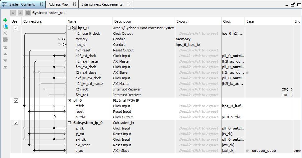
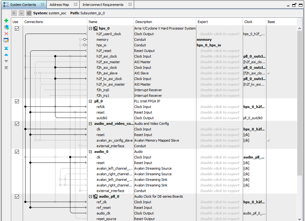
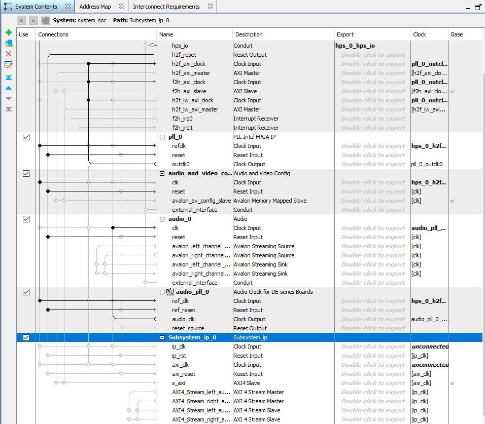
The IP cores were added to the reference design with the following settings
The reference qsys file after adding the audio IP cores is shown below.
The following lines were added to the plugin_rd.m file to add an AXI4Interface:
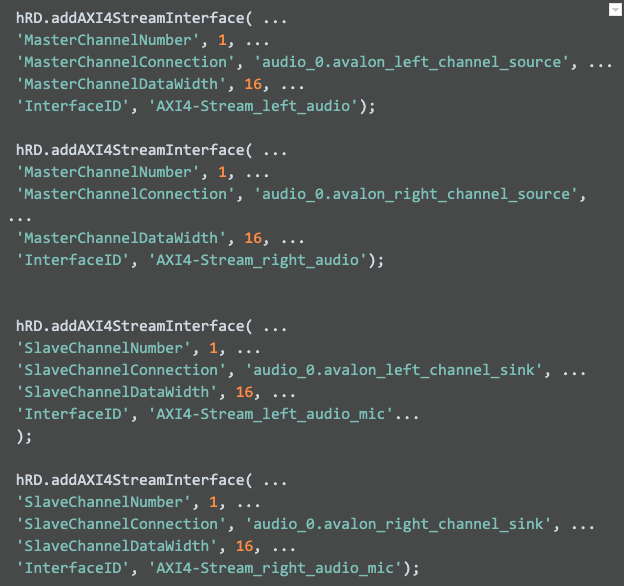
We were able to generate the IP core but the workflow failed in the Qsys integration phase. This was because the Simulink Model supports only an AXI4 streaming interface and the Audio core supports an Avalon Streaming interface. It is not possible to interconnect the two directly over Qsys. We did not attempt to proceed with this.
The qsys file in which the subsystem was automatically added by HDL workflow advisor is shown below.
Results
We were able to successfully setup the softwares and packages and run the demo system. But the large number of software dependencies meant that the work was non-trivial. All software and packages had to be of specific versions, including MATLAB and with proper licenses. For example, a Quartus trial licenses completes the workflow successfully, but does not generate the output files. It also does not show an error, which made it difficult to diagnose the issue. Controlling the LED blinking pattern and frequency from SImulink ensured that the complete toolchain is working and that all hardware setup is validated. This step was quite important as we were using the workflow for the first time. This ensured that we could focus on the Simulink system modelling in the next phase and isolate any issues to be within the model and not in the setup.
The familiarity with the Lorenz ODE solver system during the LAB aided us in most of the design decisions. The type of fixed point data representation to be used, overflow considerations and expected outputs were already known. The significant work involved was in familiarising with the Simulink Design flow and types of blocks. The fixed point arithmetic part was significantly easier with Simulink than verilog due to built-in capabilities. One issue was that in many cases the Simulink built in models may not be sufficient. For example, in the accumulator we need the initial value to be an external input. But simulink accumulator block does not support this. This meant that a new accumulator had to be design from fundamental blocks. Another issue was that not all Simulink blocks are synthesizable and one should be careful in choosing the blocks. Otherwise they may work in simulation and fail in synthesis. in such cases, we should consider rebuilding the block in a synthesizable format with fundamental blocks. The ability to simulate the system completely in simulink before synthesis, helped us debug the issues faster. We were able to implement and test the Lorenz ODE solver with full user control over all parameters and visualize the outputs.
The third phase of the project was rather ambitious and required much more knowledge of AXI and Avalon interfaces than we anticipated. Also the documentation and support from MATLAB for this was scant for INTEL SoC. However, a comparatively better documentation exists for doing this for Xilinx devices. Looking back, some of the things that we could have tried out was to find an IP core to interface the Avalon and AXI bus or use the workflow partially to generate the custom IP and then add it into Qsys and do the integration with audio system by exporting all signals to the FPGA fabric.
Conclusion
Overall the project was successful. All software and packages were setup. Workflow and hardware setup were validated using demo system. A Lorenz ODE system was completely designed in Simulink. The design was tested in both Simulation and after synthesis with FPGA-in-the loop. The waveforms obtained were verified and were comparable to the ones obtained from the benchmark system. The real-time variation in waveforms on display, while varying parameter in Simulink (with the model running on FPGA) was verified. The third phase could not be completed due to software limitation. Nevertheless, the learning from the process was significant.
The project was a huge learning experience though the learning curve was high. Even though the Lorenz system is a relatively easier system, the experience gained from implementing the system was significant. This would ensure that the implementing much larger systems would be relatively easier in the context of these learnings. Some of the pros and cons of this approach are listed below:
Pros:
- Highly intuitive design flow
- Block level visualisation of system ensures correct connections and reduces chances of mistakes.
- Highly portable. The simulink design can be deployed on any FPGA platform with only changes to the toolchain.
- Large number of ready to use blocks.
- Ability to fully simulate the system
- Does not require any coding
Cons:
- Software setup is non-trivial. (But one time job)
- Documentation is slightly obscure for Intel Devices. (But a larger number of examples are available for Xilinx devices).
- Not all Simulink blocks are synthesizable.
- In some instances, verilog code may be easier than a block level model as we have finer control.
Appendix
Appendix A - Project Inclusion
- The group approves this report for inclusion on the course website.
- The group approves the video for inclusion on the course youtube channel.
Appendix B - Work Distribution
We worked closely together throughout the project. We worked on all the software setup, Simulink modelling, and troubleshooting together in the lab. When writing the final report, we split the parts and worked on different sections of the website through Google Docs remotely.
Appendix C - References
External References
- Course Website
- Lorenz ODE Equations - Wikipedia
- Model-Based Design for Targeting Hardware-Software Applications
- Setting up Terasic DE1-SoC for Simulink
- Getting Started with Hardware-Software Co-Design Workflow for Intel SoC Devices
- Running an audio filter on live audio input using a Zynq board
- 3D Scope