Introduction
This aim of this project was to develop a hand gesture tracking system using OpenCV using a Field Programmable Gate Array (FPGA) as an embedded system. Often, individuals exercising certain parts of their arms move incorrectly and without any feedback. Thus, the motivation for this project was to recognize particular hand gestures and provide meaningful, corrective feedback to the user.
This project uses a 3D stereographic camera, a DE1-SoC Cyclone V FPGA paired with a dual core ARM-A9 hard processor system(HPS) and a VGA set up to perform marker detection, simple gesture recognition and 3D anaglyph video output using OpenCV. The project was broken into the following parts: 1) System set up including installation of OpenCV, 2) Marker Detection using OpenCV, 3) FPGA Architecture to stream and process video using on and off chip memory, 4) Feedback for gestures using both the FPGA and HPS.
High Level Design
Overall, this system tracks markers on a moving object in real-time. The design utilized both the FPGA and HPS to process and handle video input and output. We used the HPS to run external software including OpenCV and to perform the marker detection, while we used the FPGA to stream anaglyph video and determine feedback on user movements. The block diagram below describes the roles of the FPGA and HPS as well as intermediary hardware used to increase processing of images.
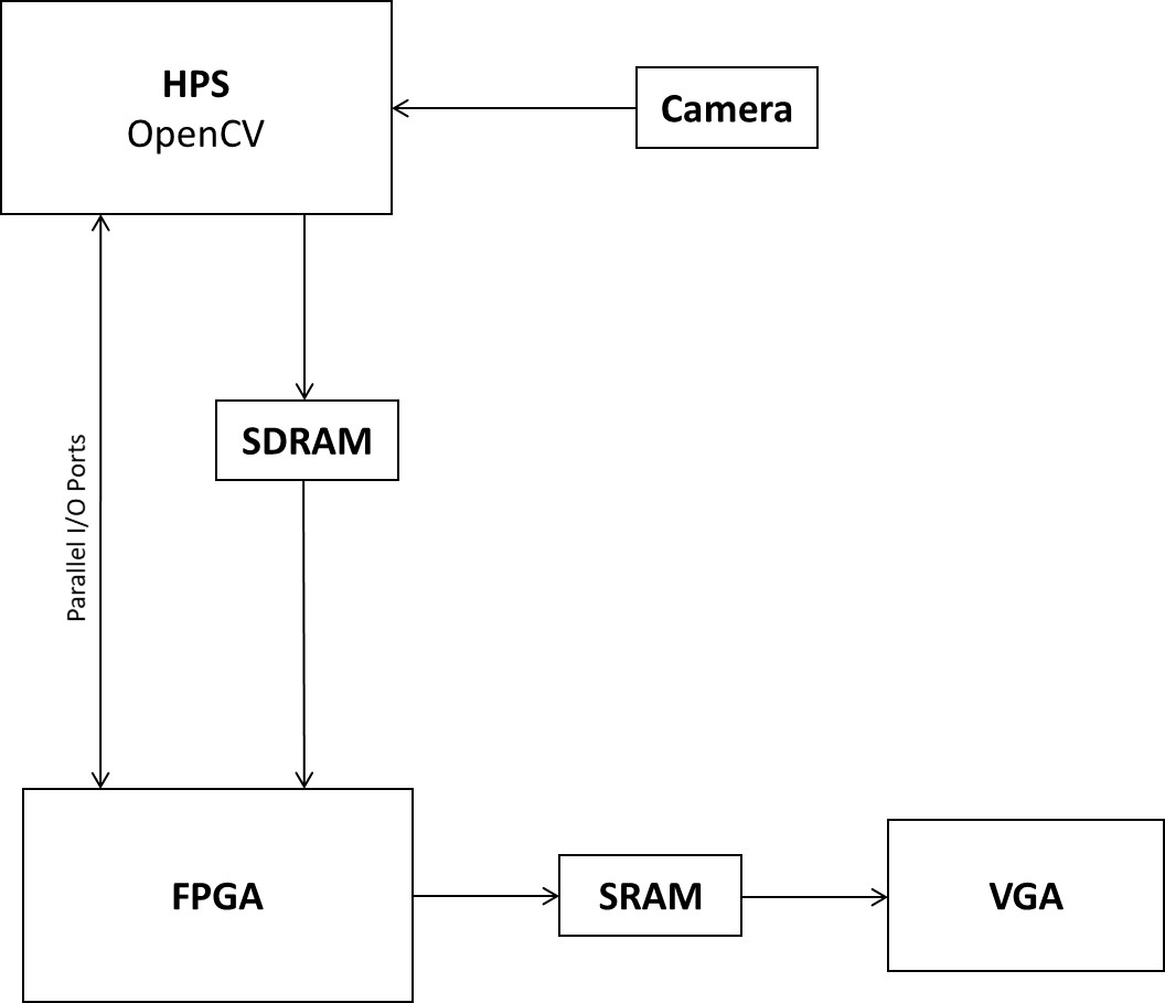
HPS Components
Video Input: USB camera’s interface well with Linux systems, and OpenCV was able to read the video captures with little configuration so input streams were handled on the HPS side. The input video was in the form of data streams not visual, video streams.
Marker Detection: Markers were detected using the Aruco Module within OpenCV. The detection and processing of markers was done on the HPS because the libraries were easier and faster to use than directly implementing detection on the FPGA. This also allowed us to use more complex markers.
User Interface: Directional feedback such as telling the user to move up and down, logging of marker detected and relevant feedback from the FPGA and writing this information to the VGA system was handled by the HPS.
FPGA Components
Memory Interfaces: We developed an interface with off-chip memory so the HPS could quickly write and the FPGA could quickly read images. To write to the VGA, on chip memory was necessary to write pixel colors. For this, we used SRAM to process anaglyph images produced directly on the FPGA.
Feedback: Given x, y and z coordinates (z being depth), the FPGA kept track of changes in position in either the y or z direction (lateral or depth movements) and sent directional signals back to the HPS. It also performed calibration to measure of a baseline/starting position of the user.

Hardware/Software Tradeoffs
The major trade-off that had to be addressed in this project was the division of labor between the HPS and FPGA. It is a natural choice to do difficult image processing and marker detection on the HPS because libraries like OpenCV exist. Implementing these algorithms from scratch on the FPGA would minorly accelerate the process but would be far more time consuming. Additionally, this project explores the use of the FPGA as an embedded system rather than a hardware accelerator. As a result, the FPGA mainly handles memory management and video processing which occurs more quickly and efficiently on the FPGA than on the HPS.
Existing Work and Standards
There are numerous embedded system designs for movement and gesture recognition including projects on the Raspberry Pi as well FPGAs. This project stands as a proof of concept and combines various design choices from the projects described including the use of OpenCV. This project adheres to VGA Standards and outputs videos based on these standards.
Implementation
Linux Set Up
In order to make OpenCV installation easier, we used a Ubuntu 16.04 image instead of the Linux setup provided in class. The Terasic Website provides a disk image (CD-ROM section) for Altera DE1-SoC boards (rev.F board). A 16 GB SD card is necessary to store the image and run the operating system on the FPGA itself. The default image settings on the SD Card include 4 GB of memory for the HPS filesystem, approximately 2 GB for the operating system itself and the remaining as unallocated space. Initially, we used this default and the SD card we had been using through the semester (which had the same partitioning) to install OpenCV and necessary packages. However, we found that the OpenCV build constantly failed because the filesystem size was too small. Additionally, creating a swap file with the 4 GB of memory would still not leave enough room for our project files. A swap file is essentially space on the hard disk that is treated as virtual memory so the operating system can mimic the RAM. To create one, the filesystem size needed to be increased. Consequently, we used a 64 bit Windows 10 Operating System to set up the SD Card and went through the following steps to successfully set up OpenCV:
- The Linux image described above was downloaded and extracted.The image was written to a 16 GB SD Card with the Win32 Disk Imager tool.
- To extend the filesystem partition (FAT32 or FAT16 filesystem), GParted Live was used. This software can be used on Linux via the install instructions on the website. However, for a Windows system, the i686 stable release must be downloaded. GParted Live is preferred over other partitioning tools because it does not wipe away the data on SD Card, while we found various other tools would reformat the disk.
- The bootable image must then be written to a USB (we used a 32 GB USB, but 8-16 GB works as well) following these directions.
- To boot the program on Windows, the BIOS must be setup. Restart the computer to enter the BIOS settings (this is based on the computer model). In the Boot menu, add the USB/GParted Disk to the list of bootable devices and add it to the top of the boot order. This ensures that the program will automatically boot when the system is restarted.
- Further details and help on BIOS settings can be found here.
Once the GParted Live was running, we inserted the SD card and re-partitioned the disk such that all the unallocated memory was allocated to the 4 GB FAT32 filesystem. This tutorial was helpful in actually partitioning. Once the SD Card was ready, the Ubuntu Linux was set up on the FPGA with the following steps:
- We downloaded the “Linux Ubuntu Desktop” Board Support Package (4.5 kernel) which contains example projects to run on the FPGA.
- The project in Demonstrations/SOC_FPGA/DE1_SOC_Linux_FB directory contains a .sof file that can be directly compiled onto the FPGA.
- The FPGA can be set up with a mouse and keyboard with the two USB ports and a VGA screen. With this setup, the programmed FPGA should boot up Ubuntu with a full desktop set up.
- Note that we used this Ubuntu setup for debugging purposes and to set up OpenCV and the camera. The actual system was built on a custom project.
Camera
First, we tried a DMC GF5 Panasonic Stereo Camera. While we were able to acquire the right and left images to then process into a stereo image, there was no video or streaming support. So, we ordered the SVPRO Synchronization 3D VR USB 2.0 MJPEG 60 FPS which supported real time, 3D video, images and stream. The camera had a right and left fisheye lens so two video streams were generated. Because the camera was not supported on Windows, we first tested the SVPRO on a 3D Camera Android App (any 3D camera app works) on an Android device, and were able to capture video successfully. To access the camera on the FPGA, we connected the camera via USB and were able to check if the system recognized it in the devices folder. We were not able to use the camera for the initial Linux version, due to lack of UVC drivers. However, the Ubuntu setup worked well with the camera.
OpenCV
We used OpenCV for marker detection. We compiled OpenCV with the following modules:- aruco
- core
- highgui
- calib3d
- features2d
- flann
- imgcodecs
- imgproc
- video
We used the aruco module for marker detection. Aruco markers are black and white square patterns, similar to QR codes, that can be used for pose estimation. The OpenCV Aruco module can be used to identify which markers are in the image and give pixel coordinates for where they are in the image. Preconfigured markers of different sizes are stored in different Aruco dictionaries. It is possible to create custom markers in a dictionary. However, we chose to use the markers in the predefined 4 by 4 dictionary. We printed three of these markers to be used for camera detection. From the OpenCV Aruco detection, we can get the ids of the markers detected in the image, and also the location of the corners of the marker. For each marker, we would detect separately in the left and right image. This gives us two sets of (x,y) coordinates. We are able to get coordinates for all four corners of the marker. We chose to take the (x,y) coordinates of the top left corner and use it to compute the depth, z. The z coordinate is estimated by taking the inverse of the disparity between the x values in the two images (1000/(|x2-x1|).
HPS to FPGA via SDRAM
Since two video streams are generated (right and left), we chose to create an anaglyph stream and process the images on the FPGA itself. In order to continuously write 240x320 frames quickly, each left and right incoming frame was written to SDRAM by the HPS. Then, the FPGA could read the SDRAM via a custom bus master.
To use the SDRAM, we used the ECE 5760 SDRAM Bus Master example as well as the SDRAM Guide provided by Altera. The SDRAM itself is off the chip and has a capacity of 64 MB suggesting we could fit approximately thirty 8 bit frames (right and left) at a time. Writing to SDRAM from the HPS requires memory mapping a virtual address to the physical address space, and using memcpy to write the images into memory. On the FPGA side, the SDRAM had to be read through a custom bus master designed in QSYS.
HPS: As input video is captured through OpenCV through a Mat object, the image is split into left and right images. The two images are then scaled. To write both these images to memory such that the FPGA could synchronously read each right and left pixel, we created an image array that compressed each left and right 8 bit RGB pixel value for a particular coordinate into a 16 bit short. Because the OpenCV data format was an 8 bit unsigned char for a 3 color channel (red, blue, green), each RGB value was pulled and converted to an 8 bit pixel color. This was done for the right and left image, and then compressed into a 16 bit value. The 16 bit value was then stored in an image array. 16 bits was chosen as the default because the SDRAM was internally configured to handle 16 bit data.
Qsys: To read the images in memory, the FPGA cannot directly read from the SDRAM. An Avalon Bus-Master peripheral must be set up to drive the SDRAM to abstract out the off-chip memory block. We set up an External Bus to Avalon Bridge (EBAB) with the avalon_master connected to the avalon slave of the SDRAM. Qsys generates a series of external signals that allow us to interface with the SDRAM. These signals include an address, read/write signals, read/write data and bus acknowledge that signals the bus is ready to read/write. The bus master shares a clock and reset with the computer system and HPS.
FPGA: The FPGA interfaces only with the bus master, named Bus_master_video. If the bus master is ready (bus acknowledge is high), the top level state machine (described above) will read memory corresponding to a pixel in position (x, y). The data will be split into RGB values for both the right and left images. All of this occurs in one clock cycle because the address is set in the previous state (when the previous coordinate is being drawn). Once the pixel color values are stored in registers, we are ready to write to the VGA.
FPGA Draws to VGA
Qsys: A dual-port, dual clock SRAM module named “onchip_vga_buffer” was used to stream the anaglyph images that were produced from the video stream from the SDRAM. The second memory mapped slave is wired to the pixel_dma_master in the VGA Subsystem, which handles the writing to the screen given pixel colors. The module shares a clock and reset with the Computer System and HPS, and the other slave port is exported so the FPGA can write data. Note that the default OnChip_SRAM module cannot be removed because the HPS seems to use it for an unknown reason. We observed that unwiring it or using it instead of our own SRAM module, prevented any drawing from occurring.
FPGA: An 8 bit combination of RGB values from the right and left image to write to the 8 bit pixel color. In one clock cycle, we write the 8 bit combination to an SRAM corresponding to the (x,y) coordinate/location of the SDRAM image.
The Qsys and module designs are shown below.Anaglyph Versions
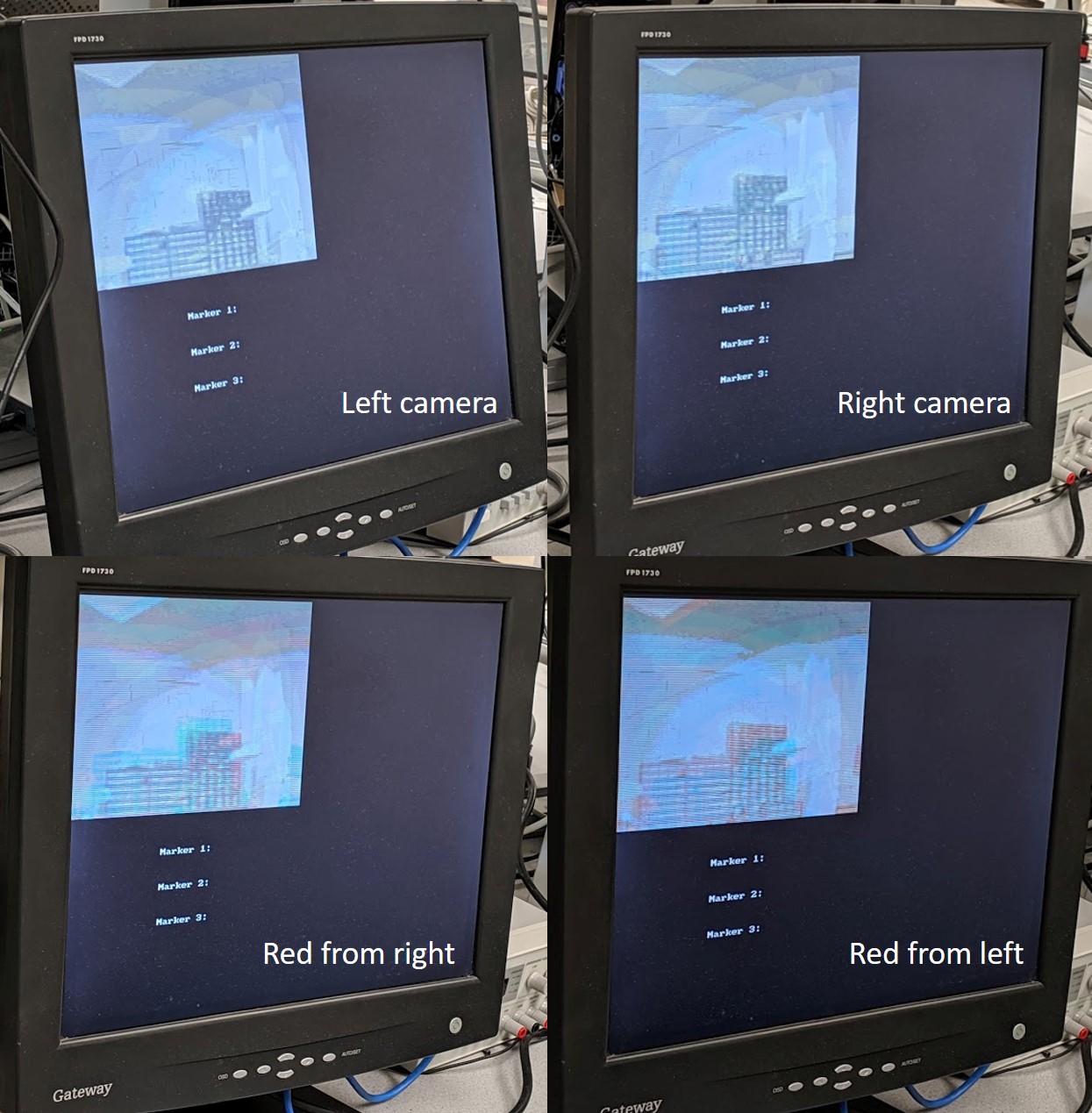
To create anaglyphs and different image types, we used switches on the board to set the output of the stream. To create the anaglyphs, we put together either the red pixel color of right image with the blue and green of the left image, or vice versa. All the possible outputs are listed in the table below.

Top Level State Machine
The Top Level State Machine (pictured below) uniquely controls the stream between the SDRAM and SRAM. The state machine describes the flow at a high level. Here, it is important to note that we cut the number of clock cycles in half (from 4 to 2) by setting the SDRAM address when we write to SRAM and vice versa. Though, we’re running at CLOCK_50, this still marginally increases the rate at which frames are being read and written.
When we write to SRAM, we also increment out current x and y coordinates to determine the next SDRAM address. The range for the x was 320 and the range for the y was 240 in order to create a 320x240 display in the top left corner of the VGA screen. Once every pixel in a frame was computed, the coordinates would get reset. The SDRAM address was computed by adding a 32 bit x value with a 32 bit y value scaled to 320. The SRAM address was computed when the SDRAM was being read from. Same as the SDRAM, we use the x and y coordinates to determine an address offset which is added to a base memory address (0) to render an image of matching dimensions.

Feedback Mechanism
A simple way to provide feedback to the user is by correcting the stability of their movement. For example, if a marker starts at position (0, 0, 0), once it has completed a movement, it should return to position (0, 0, 0). Similarly, with a hand movement, a complete and correct movement assumes starting and ending in the same location.
Calibration
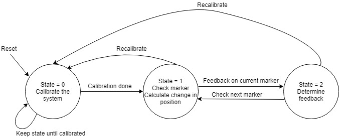
To determine an approximate starting position of the three markers, we had an option to calibrate and reset the system. To calibrate, we essentially take the average starting coordinates of some number of frames of video stream (we tried 16, 32 or 128 frames). When KEY[0] is pressed, a counter keeps track of the number of frames captured, and for each x_start, y_start, z_start, the current x, y, z is added. Once the frames have been captured, all the starting position are bit shifted by the corresponding power of 2 (4, 5 or 7) and used as the baseline to compute change in position.
Feedback State Machine
Given the starting (x, y, z), a predefined threshold is used to compute change in vertical distance (y) or depth. Take the example of the y direction. For each coordinate, the absolute difference in the current y position and the starting y position is compared to a predefined threshold. If the displacement is outside the bounds of the threshold, the feedback signal will send either a “move up” or “move down” signal based on if the difference is positive or negative. If the difference is positive, the user should receive a “move down,” if negative, then “move up” and otherwise, the feedback will say “stay still.” The threshold is equivalent to the number of pixels moved in a particular direction. This value needs to be tuned and further details can be found in the testing section. The state machine for this mechanism is depicted below.
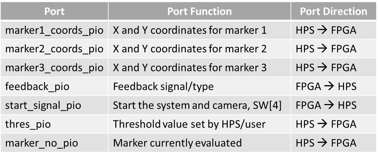
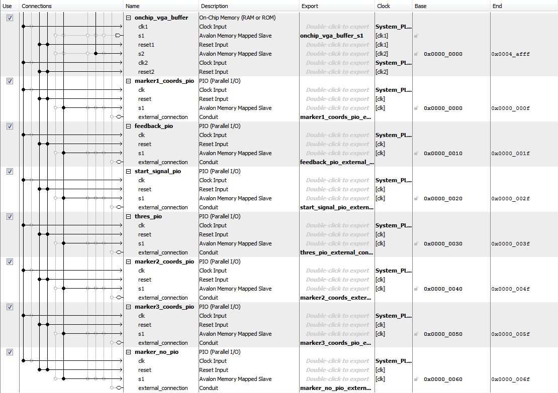
Parallel I/O Ports
To constantly read the (x, y, z), we set up a single ported, 24 bit parallel port for each marker and sent each 8 bit coordinate in one go. To keep track of which marker we were actually evaluating, the marker number was sent via a 2 bit parallel port. We also have ports for the threshold, feedback and start switch to start the system. These are detailed below.
Testing and Results
Marker Detection
To first test the marker detection, we printed out an Aruco Checkerboard using a pattern generator, and used the Linux Ubuntu SetUp to see if the markers were actually detected. Ubuntu allowed us to use the video viewing gui so we could accurately see if correct markers were being detected in both the right and left images. We used this set up to also test matching markers between the right and left images.
Once we were confident that the detection was working, we kept the Linux Ubuntu image but did not use the VGA set up, Desktop GUI or video GUI. We mostly used print statements on the coordinates to debug the remaining data processing.
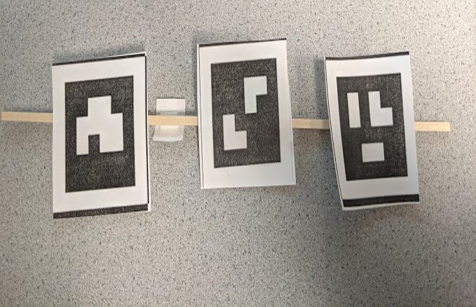
Once we had video streaming on the VGA from the FPGA, we tested markers using both the HPS interface and SignalTap on the FPGA side. We put three markers on a thin, wooden stick (picture below) to mimic arm movements and used print statements on coordinates, feedback and marker ids to check if detection and feedback was working correctly.
Memory Interfaces
On the FPGA side, we primarily used SignalTap and the VGA display to debug the Top Level State Machines. The biggest issues we faced were the following:- In the examples we used, memory addresses for the SRAM were in two forms - compressed or uncompressed - depending on if we were using ECE 5760 examples or Altera’s examples. We were able to gauge incorrect memory mapping on the VGA itself because the dimensions being drawn on the VGA were skewed. We saw a pixels being written to 320x420 dimensions suggesting values were being skipped or the address was incorrect We also used SignalTap to check if the x and y coordinates of the image (which was mapped to the SRAM address) was correctly incrementing. We ended up using the compressed format for the SRAM address (bit shifting the y coordinate) and the uncompressed format for the SDRAM address (scaling the y coordinate).
- We also had issues in our Qsys setup, and these were harder to debug because SignalTap would not let us signal into the SDRAM module itself. We were missing a bus master as the interface between the FPGA and SDRAM.
- Another issue we faced was that the ARM 9 wiring to the SDRAM also relies on wiring to the On Chip SRAM (for an unknown reason). Originally, we used the default SRAM block as our VGA buffer, but this caused the pixel values to be read and written incorrectly. We debugged this mostly by going through our wiring logic and trying different combinations of modules. We found that by completely isolating the SRAM VGA buffer from the HPS, we were able to get a relatively clean stream.
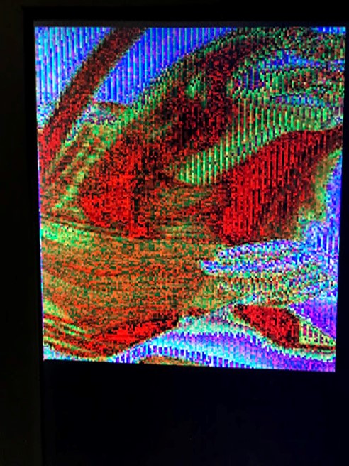
- An example of noisey input is shown below. Smaller issues we faced were incorrect memory mapping on the HPS side, initializing incorrect byte-enable in the Bus Master and SRAM and smaller issues in incrementing our x and y values. These were debugged mainly through print statements and SignalTap.
Thresholding and Feedback
To have a functioning UI and application for the project, we needed the feedback system to work accurately. However, determining the threshold for change in displacement proved to be extremely difficult. Because the threshold value is the change in pixel coordinates, it becomes dependent on how far the user or markers are from the camera. To determine threshold values at various distances, we manually tested. We observed that if the markers are further away (approximately 2 feet), the threshold in movement decreases. This makes sense because the change in coordinates would be smaller since the marker looks smaller (from the perspective of the camera). However, putting the markers closer to the camera (approximately 6 inches), causes the threshold to be much more sensitive and sporadic.
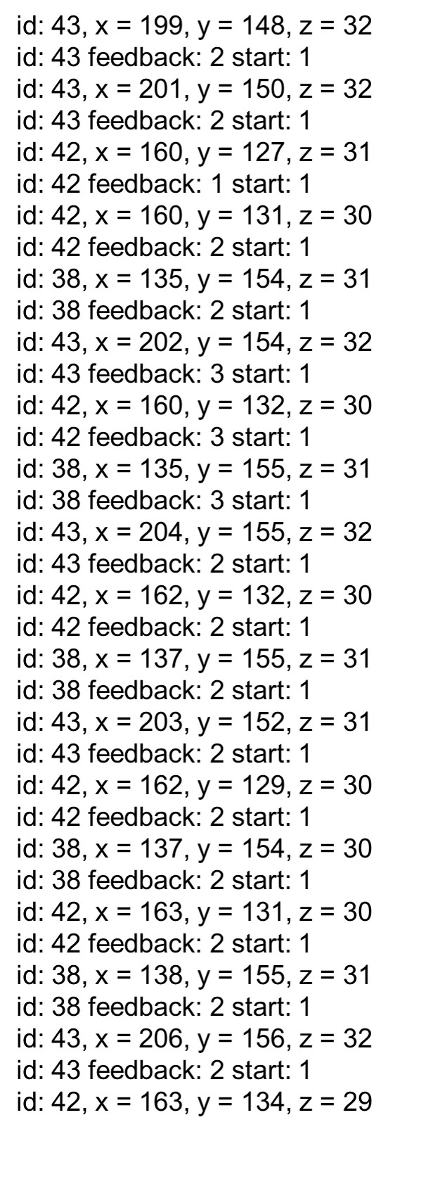
We found that a good range for these distances was between 8 - 20 pixels for the y direction and around 1-4 pixels for the z direction depending on the location of the markers/users. To determine this, we ran the HPS code multiple times and logged the x, y and z coordinates to manually look at the change in the y and z coordinates. An example of the logged data is shown below. In that test, the threshold was set to 10 for the y direction. We can see that feedback was working correctly because as the markers were moved up and down, signals were being sent from the FPGA. The z direction was pretty stable (changes of only 1 to 2 pixels were calculated), but the y direction was often outside the bounds of the threshold.
Additionally, the writing from the HPS to VGA for the feedback was sporadic because the FPGA computations were extremely fast. The output was a little noisy and not completely accurate as a result. The feedback state machine would have benefitted from being clocked by the HPS to provide feedback every few coordinates per marker. This process could have also been parallelized so feedback for all the markers would be shown concurrently instead of one at a time.
Video Output
In rendering the output video, we observed a lot of ghosting and double figures/objects. A likely explanation for this is the view and range of both lenses was really wide, so the closer the object was to the camera, the more distorted it became. Examples of this are shown below.

We also observed this ghosting in the anaglyph images (with the 3D glasses on). Though the 3D effect worked, it became less apparent the farther away the object moved because the object was smaller. However, the image was much clearer. A potential reason for this could be the address mapping from the SDRAM to the SRAM. There is a possibility that if the right and left input images are not perfectly synchronized on the HPS side, pixels could be skipped and written incorrectly to memory, causing the image to be drawn with noise on the VGA.
Conclusions
Although there are some issues, this project met our expectations. We are able to fairly reliably estimate the pose of multiple markers, which can be used to infer the pose of a human. We can then track this pose to give feedback to the user. We also use our stereo camera to output 3D anaglyph video to the VGA to give the user more feedback.
There are multiple areas of improvement for this project including decreasing the distortion and ghosting and optimizing the thresholding to work for both vertical and depth displacement. The thresholding algorithm could be improved on the FPGA side by including both the x and z directions when providing feedback for more accurate results.
To improve upon this project, we would first finetune the marker detection. Aruco includes detection parameters that handle detection and rejection of markers in the image. We would then expand upon the feedback. Our current implementation only gives feedback about translation on an axis. We have also begun a collinearity check that would give a signal if the user is bending their elbow when they are not supposed to. This is done by computing the area of the triangle formed by the three markers. We can also research other types of movement checks to implement. Our project is designed to be able to easily integrate additional types of feedback.
Appendix
Demo Video
Appendix A - Approvals
The group approves this report for inclusion on the course website. The group approves the video for inclusion on the course youtube channel.
Appendix B - Code and Schematics
Verilog Top Level
HPS Detection Code
Detailed Qsys Schematic
Final RTL Design
Appendix C - References
Altera SDRAM Guide
ECE 5760 Bus Master
Other Altera and DE1 SoC Resources
Appendix D - Work Distribution
Rohit: focused on OpenCV installation/configuration, marker detection and UI (HPS components). Aasta: focused on Linux installation, memory interfaces and hardware architecture (FPGA components). Both of us worked on our respective sections in the final report, were pair-programming most of the time and were involved in testing the system together.
Acknowledgements
We would like to thank Professor Bruce Land for all his guidance and help through the semester and on the final project. Thanks to Professor Joe Skovira for helping us set up our system as well!