ECE 5760 Spring 2023 Final Design Project
By: Alexander Scotte (ajs667), Grace Zhang (gtz4), Nivant Desai (nnd25)
The objective of our design project was to design and create a hardware accelerator for a machine learning based facial recognition algorithm.
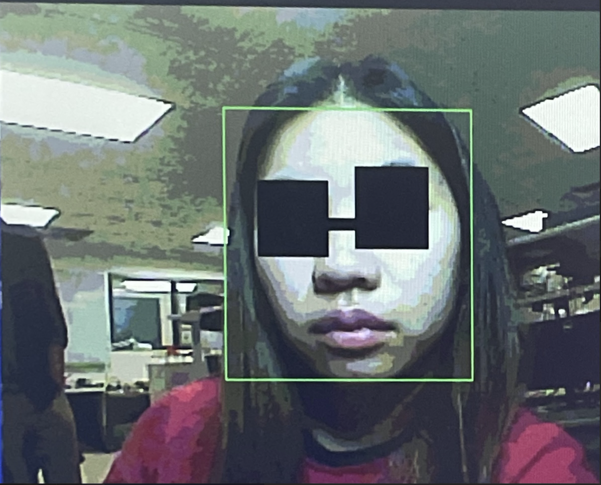
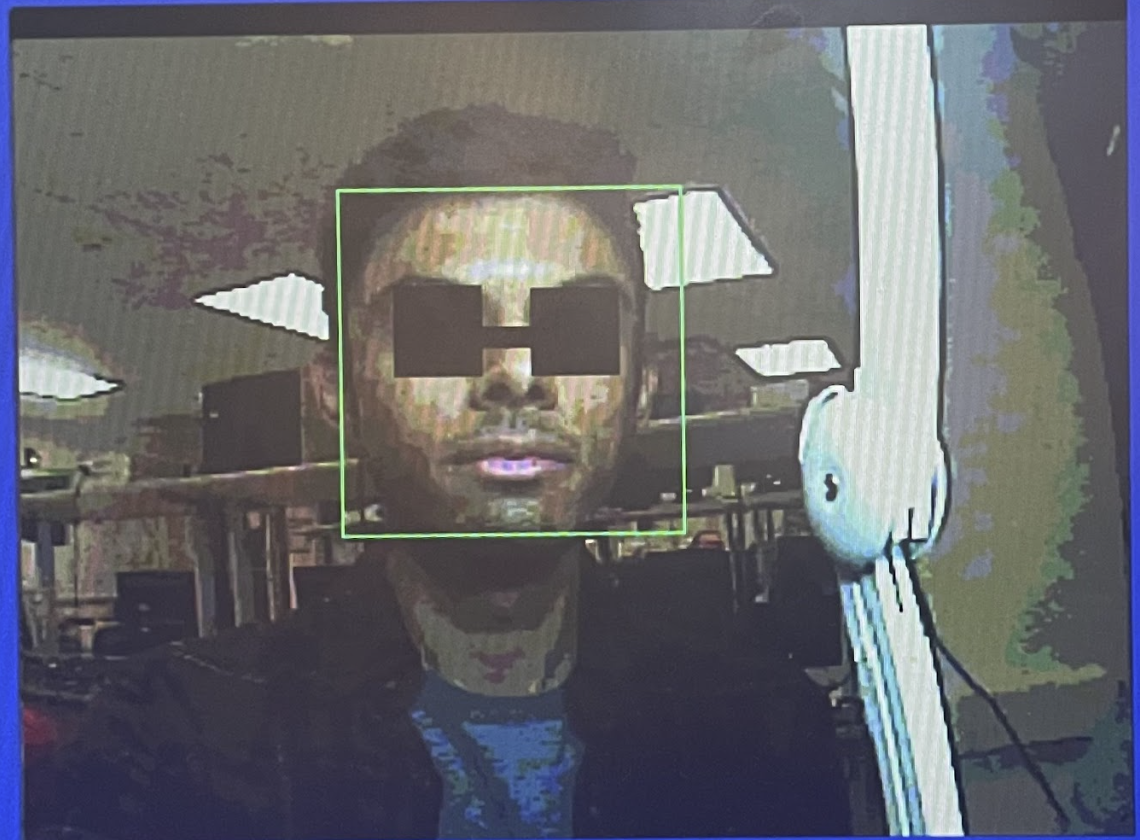
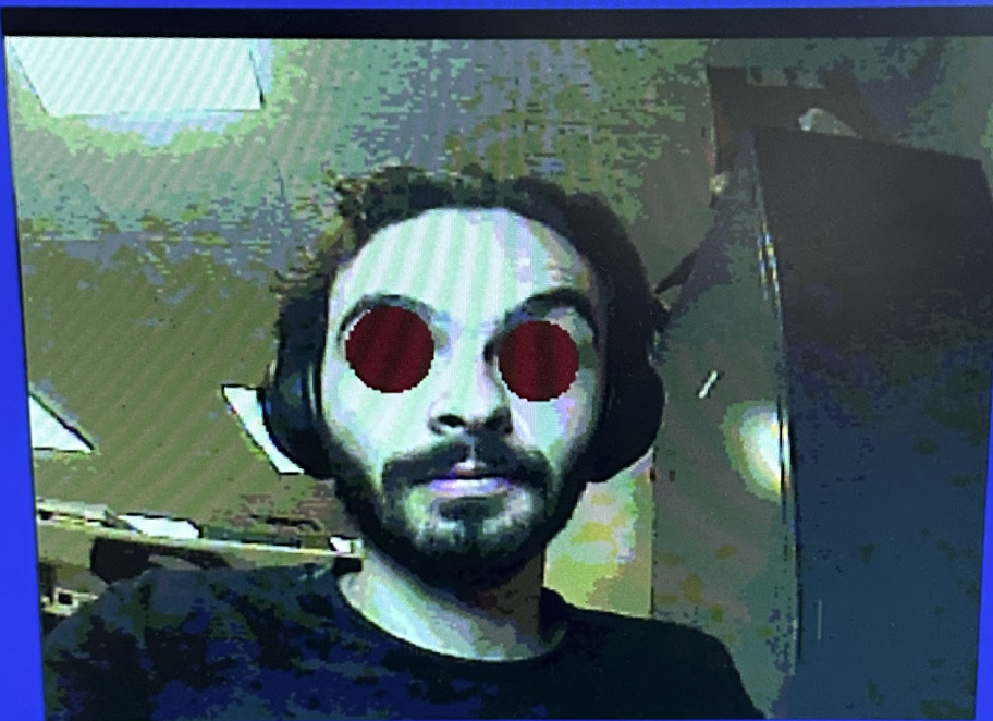
At a high level, our design operates by using the FPGA to capture video data over a VGA bus. Upon the press of a button, the user can "take a picture." This sends a single frame of video data to the ARM system on the chip, which then calculates a grayscale version of the image. This image is the input to a machine learning algorithm that is implemented in python on a computer with the ability to use OpenCV. The algorithm outputs the coordinates of detected facial features. This includes the face itself and the two eyes. These coordinates are then sent back to the FPGA, at which point a Verilog state machine is used to draw a pair of sunglasses on the detected eyes. We also demonstrate an (unused) RTL model of a preprocessing accelerator. This accelerator computes the pixel values of an integral image from a source image.
This project demonstrates the feasibility of sharing both computational processes and data between systems (consisting of the FPGA, ARM, and python systems). Distributing workloads across these systems further highlights how we might be able to accelerate traditional software level algorithms using hardware design.
Our project idea is inspired by the popularity of social media apps that exploit facial recognition to create "filters." These filters allow for pictures of people's faces to become clearer, or allow for some other alterations such as adding a pair of sunglasses. Our project aims to demonstrate how the workload for such filters may be distributed across multiple systems and thus be accelerated.
We begin with the FPGA side. The FPGA is responsible for video processing over a VGA bus, and for drawing the sunglasses. We use the VGA state machine with an external camera to display the video output of the camera to the screen. This state machine begins by reading pixel data from the video input bus in two states. It then writes this video data to the VGA memory buffer, which is then read by the ARM side to display video on the screen. This state machine executes once per pixel, each time updating which pixel will be read from the bus and written to the VGA memory. This action continues until the user pressed the first key on the DE1-SoC board. Upon pressing this button, the state machine writes each pixel of a single fram to a Qsys SRAM module. Effectively, this means that we are storing a single frame of video data to be read by the ARM side of the chip. The FPGA is also responsible for drawing a pair of sunglasses on the frozen frame using the data sent back by the machine learning algorithm. This is done by another state machine that draws to the VGA display. This state machine begins drawing black pixels at the coordinate location for the first eye. The state machine keeps drawing black pixels across the screen until it reaches the x coordinate of the opposite edge of the eye. It then repeats for the next y coordinate until it reaches the bottom of the eye. A similar process occurs for the second eye. We also send the FPGA a set of coordinates for the center of the first eye. This way, we can have additional states in the state machine which draws a black bar across the two eyes. This completes the pair of sunglasses.
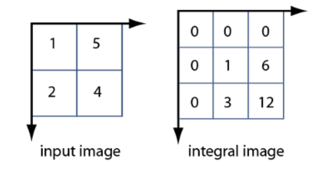
We also implemented an RTL model of an integral image calculator to demonstrate the ability of the FPGA to accelerate a preprocessing algorithm. An integral image is taken from a source image in which each pixel value is the sum of all the preceding pixel values to the top left of the given pixel. We compute the integral image from a source image using a simple state machine. The state machine reads out a set of pixels from the source image and one pixel from the integral image, performs a computation, and stores the result in an M10K block of memory. Figure 1 shows the computation of an integral image from a source image.
The ARM/HPS side of the system is responsible for reading the source image from the Qsys SRAM buffer. It does this only after the FPGA has completed storing the frozen video frame. We control this logic with a DONE flag which is sent over PIO. The HPS can then easily read out all of the pixel data and compute a grayscale version of the source image. This grayscale image is sent to the python machine learning model through the scp protocol.
Throughout the project we had to make many tradeoffs that would decrease the efficiency of the design. After failing many times to put OpenCV on the HPS we decided to go with SCP data transmission between systems. This decreased the efficiency of the design since now more than one system was involved with data manipulation. Also SCP is very slow for large amounts of data such as the images we were transmitting.
We were also not able to get the integral image working on the software side, so more calculations were needed in order to find exact facial features causing a decrease in efficiency.
To our knowledge, there are no existing patents, copyrights, and trademarks that are relevant to our project.
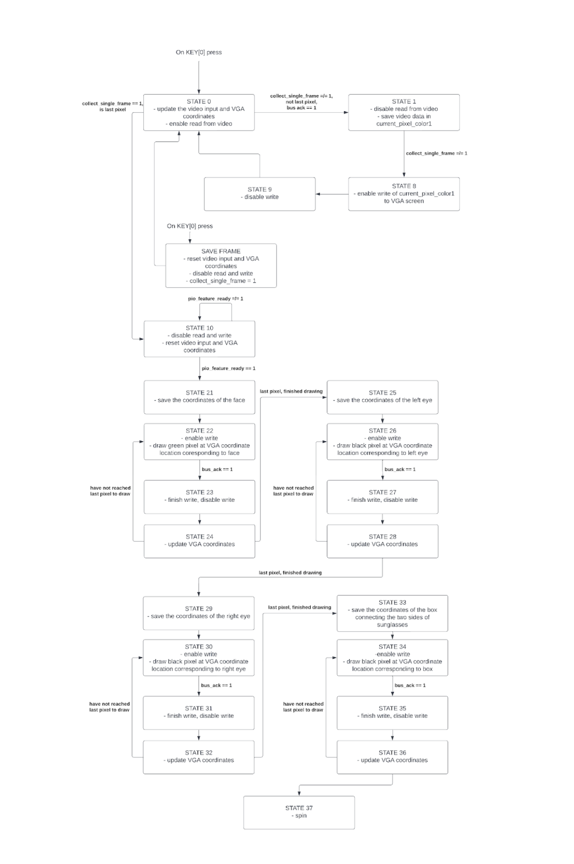
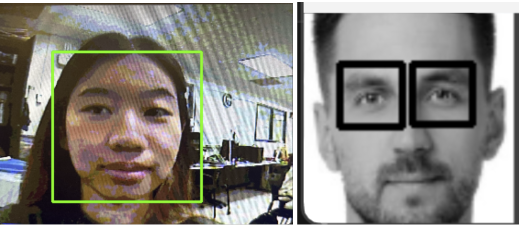
For our final design, the FPGA was responsible for displaying video input to the VGA display and pausing this video on a KEY[1] button press. After receiving data about the location of the features, the FPGA then displayed a green box around the face and added sunglasses to the onscreen image.
States 0 through 9 are from Bruce Land’s example code, Video Input with VGA output. This takes the 320x240 video input, which is stored in the SRAM, and copies the information pixel by pixel into the SDRAM, which is used by the VGA display. This is done over the QSys bus, so using an extra state to wait for an ack is crucial to making this system work. Once the image has finished copying the data for the entire image, the coordinates are reset to the top left of the video input and the process repeats.
At any point, KEY[1] may be pressed, which freezes the video display and essentially takes a “snapshot.” At this point, the coordinates of the video input and the VGA display are reset and one final loop through states 0 through 9 is done. It also sets the “collect_single_frame” flag to 1. However, upon reaching the last pixel, the state machine will then move to state 10.
In state 10, we simply wait for the model to find the features and for the HPS to send all of the information back. This was done by waiting for a flag that was set by the HPS, called pio_feature_ready. Once this is done, we move to the drawing states. States 21 through 36 are all very similar. The basic structure is 4 states based on Bruce Land’s example code above, repeated 4 times for each object that we draw – a box around the face, each of the sunglass lenses, and the connector between the sunglass lenses. The first of these states sets the VGA coordinates to the coordinates that specify the location of the desired features. Then, we draw the desired shape to the screen pixel by pixel, updating the VGA coordinate accordingly. Finally, once we have finished drawing, we move on to the next feature to draw. At the very end, the state machine goes into a spinning state until KEY[0] is pressed once again. The feature variables used for this are shown in the table below:
| Variable Name | Description |
|---|---|
| pio_feat_upper_left_x | Location of face, upper left x coordinate |
| pio_feat_upper_left_y | Location of face, upper left y coordinate |
| pio_feat_lower_right_x | Location of face, lower right x coordinate |
| pio_feat_lower_right_y | Location of face, lower right y coordinate |
| pio_ul_x_eye1 | Location of left eye, upper left x coordinate |
| pio_ul_y_eye1 | Location of left eye, upper left y coordinate |
| pio_lr_x_eye1 | Location of left eye, lower right x coordinate |
| pio_lr_y_eye1 | Location of left eye, lower right y coordinate |
| pio_ul_x_eye2 | Location of right eye, upper left x coordinate |
| pio_ul_y_eye2 | Location of right eye, upper left y coordinate |
| pio_lr_x_eye2 | Location of right eye, lower right x coordinate |
| pio_lr_y_eye2 | Location of right eye, lower right y coordinate |
| pio_center_x_eye1 | Location of center of left eye, x coordinate, used for drawing the bridge of the sunglasses |

We ran into issues with the synchronization between the hardware and software. Originally, on the KEY[1] button press, we had stored the grayscale source image into an M10K block. However, we found that when we started trying to send data over to the HPS, packets of data would be lost due to loss of synchronization. This was even the case when we attempted to implement a val/ready protocol that would only send data when the HPS was ready to receive it. Thus, we looked into storing the memory on the Qsys bus in SRAM. However, when investigating this option, we found that the VGA display memory in SDRAM stored the source image, albeit in color. Thus, to avoid duplication of the information and save space, we elected to have the HPS read the source image from the SDRAM and do the grayscale conversion on the HPS side. We did not run into any bus sharing issues, as the video input stopped being transferred to the VGA display when we needed to access the Qsys bus in the latter part of the process.
We originally implemented the integral image calculation into the project, which would greatly speed up the preprocessing. As mentioned previously in the High-Level Design section, this simply added up the source image values. However, while not a complicated calculation, the FPGA would have greatly sped up the process.
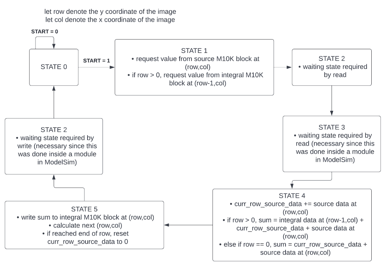
The naive solution for the integral image would be for any given pixel, loop through each of the previous pixels and sum up the values. However, this would cause the calculation of, say, the last pixel of the 320x240 image, to take at least 76800 times longer than the calculation of the first pixel. Thus, we created a new algorithm. For any given pixel, its integral value (called sum in the code) is simply the sum of the integral image of the pixel directly “above” it (aka row-1, col of the integral image) and all of the source image values that have come before it in its row (aka [0:row],col of the source image). If the pixel is in the first row, there is no need to find what the integral image value of (0,col) is, since it does not exist; we would just need the source image data for this. Because we traverse the image in rows, we can easily store the source image values that have come before the desired pixel as a cumulative sum that updates with each pixel in the row. Thus, the work for each pixel is reduced to 2 accesses to the source and integral image that can happen simultaneously, one calculation (no looping necessary for one pixel), and then a store to the integral image. This state machine is shown in Figure 4.
Note that there are a few extra states. This is because the ModelSim testbench had a master state machine that created the source image. Because of this, each read and write had to take one cycle longer than they usually need to. If this integral image calculation had been implemented in the final design, these extra states would not have been necessary.
With this design, we initially ran into many memory issues. At first, we planned to have both the 8-bit source image M10K block and the 25-bit integral image M10K block on the FPGA. The 25-bit value comes from the largest possible integral image value of 255*320*240, or 19584000 in decimal. The 320x240 image would result in 76800 indices. Thus, the number of 8-bit x 1000 M10K blocks used for the source image would be 77, and the number of 32-bit x 256 M10K blocks used for the integral image would be 300. This would be just under the threshold of 397 M10K possible blocks. However, we soon realized that we would run out of space. This is because the initial calculations of space did not take into account the Video In SRAM, which itself took up 77 M10K blocks in SRAM. Thus, instead of writing to the source M10K block and then using those values later in the integral calculation, we removed the source image M10K block, reading in from the SDRAM and doing the greyscale calculation then. Thus, we were back to 377 M10K blocks, which is under the threshold.
Another issue we would have run into had we used this (more on this in the next paragraph) would have been the same synchronization issues from before. However, this would have easily been rectified by moving the integral M10K block to the Qsys bus instead. Ultimately, we were unable to use this design as the model could not properly process an image with such large values; it was looking for an 8-bit grayscale image and we were providing it with a 25-bit grayscale image. Even though we tried scaling the 25-bit image down to an 8-bit image, this resulted in such low resolution that the model was unable to properly detect any features.
The software interface consists of two straightforward components in order to accurately determine one's facial features. Initially the data from the video data is passed from memory on the FPGA to the HPS. After some preprocessing the image is then passed over SCP in a dat file to then be passed through two models. The models are used to locate the location of the face in the picture and then the eyes. All data is then passed back through the pipeline to the FPGA in order to draw glasses on the picture located on the VGA.

In order to predict the location of the face and facial features the data needed to first be acquired from the hardware’s memory. Initially the HPS would take the image from SDRAM which also held the VGA image of the participants face. Before the image could be sent through the facial feature detection models the image needed to be pre-processed as a grayscale image. Each pixel held in SDRAM only used a maximum of 6 bits to represent RGB values and needed to be converted to an 8 bit scale. The models used to detect the facial features required 8 bit grayscale images in order to achieve the greatest possible accuracy. The Grayscale image was then saved in a dat file to be sent to the facial detection models over SCP.
The system would wait for the image to be evaluated and values to be returned, over SCP, in order to be sent to the FPGA to draw sunglasses on the participant’s eyes and draw a box around their face on the VGA. A dummy text file was sent over SCP after the evaluated data was returned in order to avoid the HPS reading the data too early causing a datarace, potentially causing incorrect values. The only way the HPS was allowed to read the evaluated data was when the text file was deemed readable by the system, and since it was sent after the data, all of the values would already be readable without any data races. Once the data was available all the values to locate the participant’s facial feature location were sent to the FPGA over a PIO port.
The facial detection system is written in python and uses pre-trained Haar cascade classifiers in a two step system. The system initiates all interactions with the FPGA through the use of SCP commands. In order to acquire data to run through the facial detection models, the script requests a dat file containing the grayscale image.
The script first uses a general face detection Haar cascade classifier to find the location of the participant’s face in the captured frame. This helps to narrow down the number of pixels needed to be analyzed to find other facial features. A more specific eye detection Haar cascade classifier is then run on a smaller number of pixels that only include the face to find the exact eye location.
Once the exact location of all of the necessary facial features are acquired, the script then saves all of the values in a dat file. All of the data is then sent over SCP to the HPS which has been waiting for values to send to the FPGA. Another empty text file is also sent over SCP to signal the image has been successfully analyzed.
The final product used SCP in order to send data to and from a set of models in order to find the facial feature locations. Our initial idea was to run OpenCV on the HPS instead of an external computer. This would have exponentially sped up the processing time in order to produce a final result. The initial problem began with trying to build a large library on a small system. Fortunately a past group was able to do this with a swap file. While we were able to generate a swap file and increase the partitions of the SD card to support the needed memory to build the library, we were unable to find the necessary dependencies that would be able to run on the ARM7 based processor.
Our second error occurred when we realized that OpenCV did not support images larger than 8 bits when calculating facial feature locations. Unfortunately the integral image needed memory that was much larger than the required 8 bit image. This caused us to change course to a normal image, instead of using an integral image in our final design.
The system as a whole takes about 10 seconds in order to compute everything necessary to display the participants face with glasses. With proper lighting and background the system can be very accurate with detecting a person's facial features. Unfortunately in improper conditions the system fails for then it succeeds.
In order to use the system one needs to first take a picture of themselves and then run the python script in order to apply the models. While the system has multiple steps to operate correctly. As a whole it is very easy to operate and achieve appropriate results in a very safe manner.
The following figures show the results of the initial ModelSim testing that was conducted. The source image is a 320x240 grayscale image where each pixel increments by a value of 0 until it reaches 255, at which point it wraps back to 0. Thus, the first few values in the source image would be 0, 1, 2, 3, 4, … and the corresponding integral image would be 0, 1, 3, 6, 10, …


The integral image would have greatly increased the speed of this project. In ModelSim, we found that the calculation for each pixel in the image took almost exactly the same amount of time to calculate (new rows necessitated double the time to calculate). Thus, we avoided having the final pixel calculation take exponentially more time than the first pixel calculation. The time to do the integral image calculation over the whole image took 9 ms in ModelSim.
Our design was able to achieve the desired final result of drawing a set of glasses on a person's face through the use of multiple machine learning models. However we were not able to use every part of the project effectively, since we were not able to integrate the integral image. Throughout the project we were able to leverage ideas and code and models from past projects and libraries as listed in Appendix D. We also followed all guidelines and standards that were applicable. In the end we were able to achieve our goal even with the errors we faced along the way.
he group approves this report for inclusion on the course website.
The group approves the video for inclusion on the course youtube channel.
Grace was responsible for the hardware design, implementation, and testing of the hardware components. This included the integral image, memory allocation, and overall state machine. She also wrote the Hardware Design portion of the design report, as well as the ModelSim section of the results portion.
Alex was responsible for developing all code on the HPS and the facial feature detection algorithm. He was also responsible for the communication between the HPS and the models through the use of SCP. He also wrote the Software design, Results, and conclusion of the report. He also created and formated the final website.
Nivant worked on the creation and testing of the hardware design. He also wrote the Introduction and High Level Design proportions of the report.
Bruce Land’s Video Input with VGA output Example Code [Quartus 18.1 (cornell.edu)]
Face finding library[OpenCV]
Idea to use OpenCV[CHARACTER RECOGNITION USING OPENCV ON DE1-SOC]
Idea to use SCP[FPGA Based Simple CNN MNIST Digit Classifier ]