Introduction
Power consumption is a critical consideration of a lot of technologies today. Phone producers, for example, always talk about their improvement in power management and how it makes their battery last longer. The balance between functionality and power is an interesting topic investigated by many. When we are doing labs, however, we rarely think about how much power we are consuming, because we are never limited by it. When we synthesized the giant drum in lab 3 for this class, we exhausted all DSP blocks on the FPGA, and we used a lot of M10K memory. This kind of extensive use of hardware is likely to result in high power consumption, and we are curious to find out what are some of the factors that could impact the power consumption of an FPGA. With this goal in mind, we built a circuit that measures the current flowing through the power-supply cable using I2C-based current sensor MIKROE-2987 while assuming a stable 12V voltage supply, and implemented an I2C receiver with integrator in the FPGA that continuously increments the energy consumed. Based on obtained data, we built an intuitive user interface on VGA showing current, real-time power, and average energy to monitor the power consumption of DE1-SoC.
Design & testing methods
Design Overview
The overall design of our power estimator is shown in Figure 1. MIKOE-2987 uses hall effect to measure current through internally fused input pins and has extreme low series resistence around 1.2m $\Omega$ which will not effect current supplied to FPGA. This board uses I2C interface by SDA for data and SCL for clock to convey obatined current data. Based on specification, we built I2C master as receiver in FPGA to convert the bitstream to actual high-resolution current data and pass it to HPS with a valid signal. This receiver also contains a multiplier and integrator to compute real-time power and accumulating energy respectively. It is controlled by HPS to implement reset, start and stop. HPS will process the obatined data and display corresponding user interface on VGA. To accelerate debugging, we also implemented 7-segment displayer to display the measured current.
Hardware design
We all know the equation $P = I * V$ for power and $W = \sum_t P * dt$ for energy from physics class, these two simple equations are the essense of this project. According to specifcation on power adaptor, stable 12V voltage is provided. In this case, real-time power is computed by one multiplier to compute $I * 12$. As for consumed power, we designed an integrator same as from Lab1 to add energy in unit time $P * dt$ on each available sample point($dt$ depends on sample rate) once computation starts. The essence for this project lies on that we need a way to measure the current provided by power adaptor so that power and energy can be computed. After some research online, we decided to go with the MIKROE-2987 current measurement board for reasons we stated above. The output of this current sensor goes to a 12-bit ADC and is provided using I2C interface using MCP3221. Therefore, we established I2C master receiver in FPGA to communicate with it.
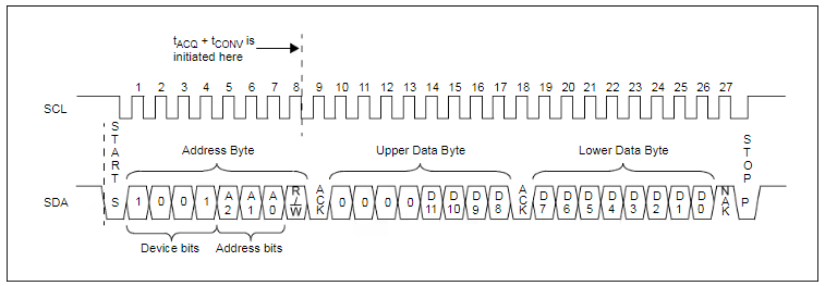
I2C protocol of MCP3221 is as shown in Figure 2. The I2C communication only involves 2 wires: SDA for data, and SCL for clock. SCL is uni-directional and provided by I2C receiver while SDA is bi-directional which can be controlled by either master(I2C receiver) or slave(MCP3221). According to the datasheet, each transaction between the master and the slave should be 8 bits long and is always followed by an ACK/NAK. When MCP3221 is not busy, both SDA and SCL will be set HIGH. To initiate data transaction, the master device has to signal a start condition by pulling down the SDA line from HIGH to LOW while SCL is HIGH. When chip is waken, it is expected to receive a address byte from master to configure the chip in SDA. First 4-bit is device bits, next 3-bit is address bit and the last bit is R/W select. We configured it to 1001_101_1 as default to read the data from chip. When a valid address byte is accepted, chip will set SDA to LOW as an ACK signal then starts to provide data. Data is provided in bytes each time. When one byte is provided, an active-low ACK from master is required so that slave can continue to provide data. Since data is in 12-bit form, two bytes which we noted as upper byte and lower byte are needed to complete one data transaction with first four bits in upper byte as zeros. With continuous ACK from master, slave will continute to provide current value without repeating the address bytes. To terminate the transaction, master can generate a NAK by pulling SDA HIGH when SCL is also HIGH, and end with a stop condition by pulling up SDA from LOW to HIGH when SCL is HIGH. It’s worth noting that changes in the SDA line should always happen when SCL is LOW, remain stable at the HIGH portion of the clock (except start and stop condition), and there should be one clock pulse per bit of data.
Based on the I2C protocol explained above, we developed an 11-state FSM in SystemVerilog which can be seen in Figure 3. In IDLE state, both SDA and SCL will be toggled. When start signal from HPS is sensed, start condition will be provided, then address byte is transmitted. When internal counter detects that address byte has been transmitted, slave acknowledge is expected. Otherwise, master will be back to IDLE state. If ACK is provided, master will receive upper and lower bytes from slave if ACK is provided after data received. In STATE_DATA_RECEIVED_UPPER and STATE_DATA_RECEIVED_LOWER, the master receives data from the slave and puts it into a 16-bit long FIFO. When HPS indicates to stop system by toggling stop signal, NACK will be provided, then stop condition will be provided and followed by a WAIT state to ensure MCP3221 is not busy any more. It is worth noting here that, since the SDA line can be controlled by both the master and the slave, we wrote a tri-state buffer to decide which device gets control of the line. The tri-state buffer comes with an enable signal that is HIGH when the master device acts as an input in the transaction, and SDA should become high impedance on the master side when this enable signal is asserted. Otherwise, SDA gets the output from master. The SCL clock line follows the input as 200K Hz clock signal whenever we’re not sending start/stop condition, not waiting, or not in idle. A data valid signal is pulled HIGH when the master acknowledges the lower bits of data or when a NAK is asserted by the master indicating correct value we can obatin from MCP3221. This signal will later be used to control our integrator in calculating accumulative energy.
From I2C receiver, we can obtain 12-bit data, however, we still need to convert it into actual current data which we set as 9.23 fixed-point data. The corresponding voltage can be computed as $data out \over 2^{12}$ * 3.3V. According to specification, sensitivity of current sensor is 110mv/A with original point at 1.65V, therefore, we can compute the actual current as $I = $ ${V-1.65V} \over 110mV/A$.

The MCP3221 I2C interface also specified that the maximum clock speed it can achieve is 400kHz, we select 200KHz which should be a reasonable choice. This means the 50MHz FPGA clock will be too fast to run, so we added a clock divider to step it down to 200kHz. As mentioned above, we went on to implement an integrator to compute accumulating energy by incrementing continuously by adding energy in unit time. We used stop signal from HPS to allow pausing of integration and start to continue. Whenever stop is not asserted and data from the I2C interface is valid, we calculate the new unit energy by computing $V * I * dt$ and add it to the total energy consumed. The value of dt was determined by counting the number of pulses between two consecutive data valid signals using SignalTap. We counted 18 pulses, which matched the protocol (16 pulses for transmitting data and 2 pulses for ACK). This means our unit energy at every new sample of current is $V * I * {18} \over {200000}$. Despite the input current using a 7.23 fixed point value, the energy output of our integrator module was set to 41.23 fixed point as 64-bit long data, because energy is accumulative so that more bits are needed to prevent overflow. However, the Qsys PIO only has a maximum bitwidth of 32 bits, so we had to create two PIO ports, one to transmit the higher 32 bit and one to transmit the lower 32 bit. We then used a long long type variable to store the 64 bit value in HPS, and later converted it from fixed point to double by a division of $2^{23}$. Doubling the number of bits also improved the precision of the reading. We also increment a counter every time the current becomes valid, and we will be able to determine the elapsed time since the FPGA starts running by computing (cycle_count - 1)*$18 \over 200000$. Here we disregard the time for the first transaction, i.e., we are not counting the first 27 cycles, because it includes time to transmit the address bits which is not representative of the transactions in between. Since our clock runs at a high frequency, these 27 cycles should be negligible, and we preserve enough precision for our time estimation.
To make debugging more intuitive, we implemented a simple segment decoder on FPGA to display measured current value. As mentioned above, current value is 9.23 fixed point, we used segment displayer 0 as sign, next two as integer and resting as fraction part. We built a mapping table using first 9-bit as integer and 4-bit among 23-bit after decimal point.
Software design
With all the needed hardware instantiated, we started to add communication with the HPS. Because our goal is to have a graphical representation of data on a VGA display, it is more convenient to work on the software side. We took an incremental approach in designing our software to guarantee correctness. We first allow the flow of data from FPGA to HPS by adding PIOs on the Qsys bus. Each PIO is given an offset from the lightweight AXI master, and we were able to access the data by looking at address: offset + lightweight AXI master address. Since the output from our integrator module is energy instead of power, we need to do some conversions. The dynamic power at every given instance equals instantaneous current * 12V, and the average power equals accumulated energy/total time spent. Before actually plotting these data, we want to make sure our data make sense, so we print the value of current, dynamic power, average power, cycle count, and time on our serial monitor whenever the data valid signal is pulled HIGH. In this process, we realized that we need to intentionally put our program to sleep for some time, because the HPS is running at a much faster rate than the FPGA, so one HIGH portion of the data valid signal would correspond to hundreds of cycles for the HPS, thus generate a lot more data points than needed. After confirming the correctness of our data, we need a proper way to display it. We decided to display three graphs on the VGA: current vs. time, dynamic power vs. time, and average power vs. time. We limit the time scale on screen to 3 seconds, meaning the graphs would be erased and redrawn using new data every 3 seconds. The y-axis scale is determined by the variable. For current, it is limited by the capability of our current sensor, which can handle up to 2A. For dynamic power and average power, the maximum is $I_{Max} * V_{Max} = 2 * 12 = 24 W$. So, from the bottom of the y-axis, every addition of pixel in the y direction represents a $24 \over 119$ W increase in power. We also created a text box to the right of the screen to display the actual value of these variables. Our final VGA display interface can be seen in Figure 4.
After being able to plot the data on VGA, we start to transition more control to the HPS side. We first disabled the button control of the start, stop, and calibration signal, and adopted a pure software control. This requires a user interface that detects input from keyboard, and we were able to achieve it by using multiple pthreads. A user is able to choose a number between 1-3, and each corresponds to pressing reset, stop, or calibrate. When a stop is detected, the drawing will immediately stop and data display freezes, and a start resumes the drawing. Calibration, on the other hand, clears the energy and time data and starts them from 0 again. All graphs will clear and immediately start redrawing when calibration is selected. A demonstration of the effect of calibration is presented in the video below.
Testing strategy
To ensure all modules in our design work as expected, we took on a hierarchical approach to testing. At the lowest level, we first tested our I2C state machine by writing a testbench that feeds in control signal, clock, and data according to I2C protocol above, and verified the output waveforms in ModelSim. As seen in Figure 5, the master is able to send out the correct address bits, generate ACKs when appropriate, read the input data and pull the data valid signal high when a 12-bit transaction completes.

After the I2C interface was proved to be functional in simulation, we instantiated the modules in Quartus and verified signal feedback from the FPGA using SignalTap. SignalTap creates the real hardware circuit in the FPGA and gives us the actual output waveform generated by our circuit. While using SignalTap, we were using current source from lab to directly feed current to the current sensor, so we know exactly what value to expect from the current output. We were also using buttons on the FPGA to control the reset, start and stop signal here, so we can easily trigger data capture for SignalTap. By comparing the current output on the power supply to the data output from SignalTap, we know whether our implementation is done correctly.
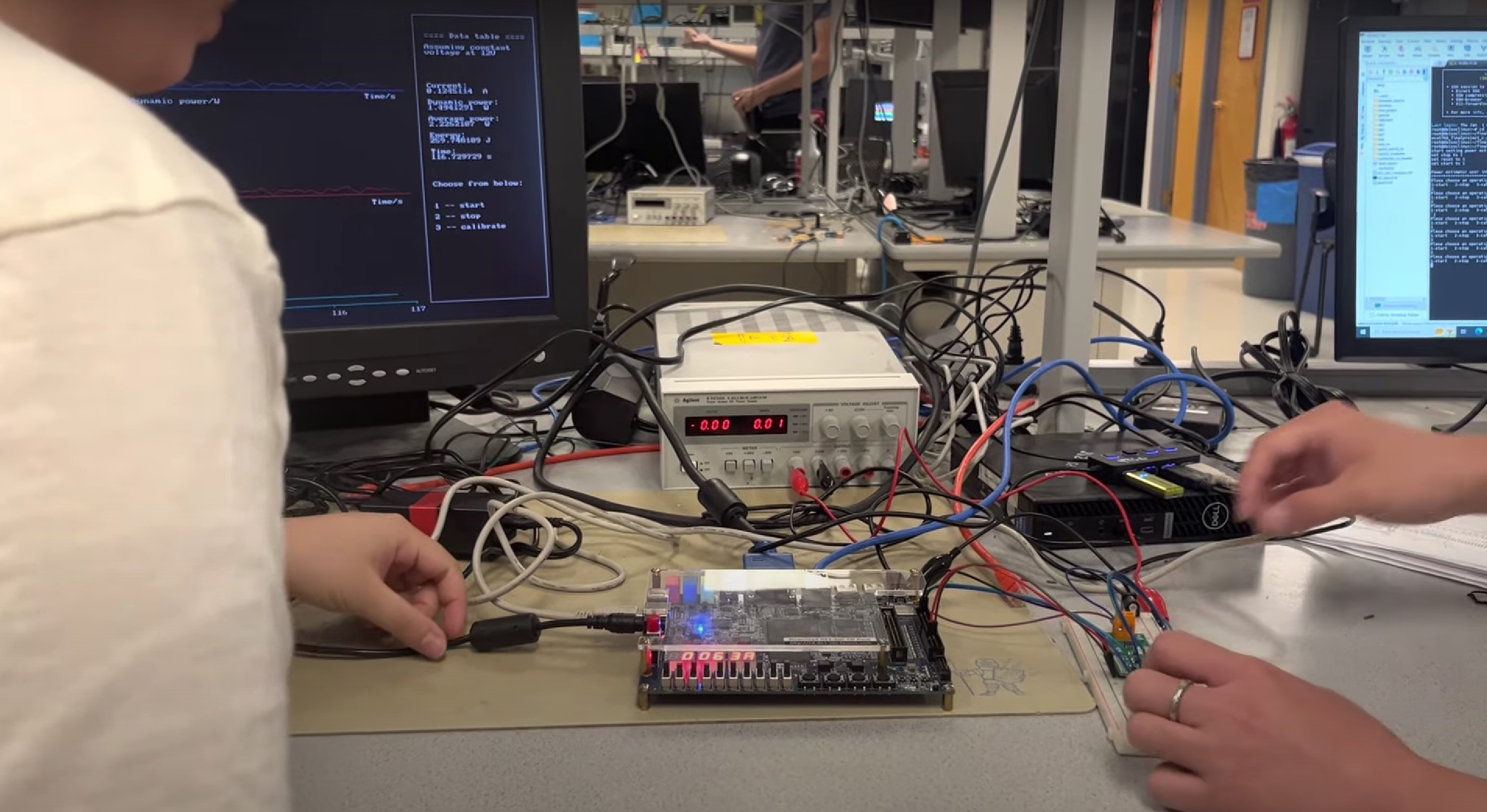
At the end of the project, we moved from using current source to directly measure current drawn by the FPGA. We placed a 2.1mm female DC power jack on a breadboard and connect to it the FPGA power adapter. The power pin of the power jack is connected to the P+ pin of the mikroe-2987 board using a jumper wire, current will pass through the board and reach its P- pin, where we connected another jumper wire to the positive end of a male jack to open end power cable. The male power jack is inserted to the FPGA, whereas it negative end is connected back to the ground pin of the female power jack on the breadboard. This setup forms a series circuit where the current measured by the current sensor should be the same as the current drawn by the FPGA. Figures 6 and 7 show how we set up this series circuit. We observe the graphs and different readings on screen to see if the data makes sense. We observed fairly constant reading of current and power in this setting, which is expected because the FPGA is always running the same program. We also switched to using pure software control instead of buttons at this stage, and we compare the behavior of the VGA output when asserting signals in software to what was expected. We were able to see stopping of graphs when stop is selected and resume of drawing at start. Calibration also works correctly as graphs were erased and time axes reset properly, and the data display of current and energy goes back to 0.
Results & Analysis
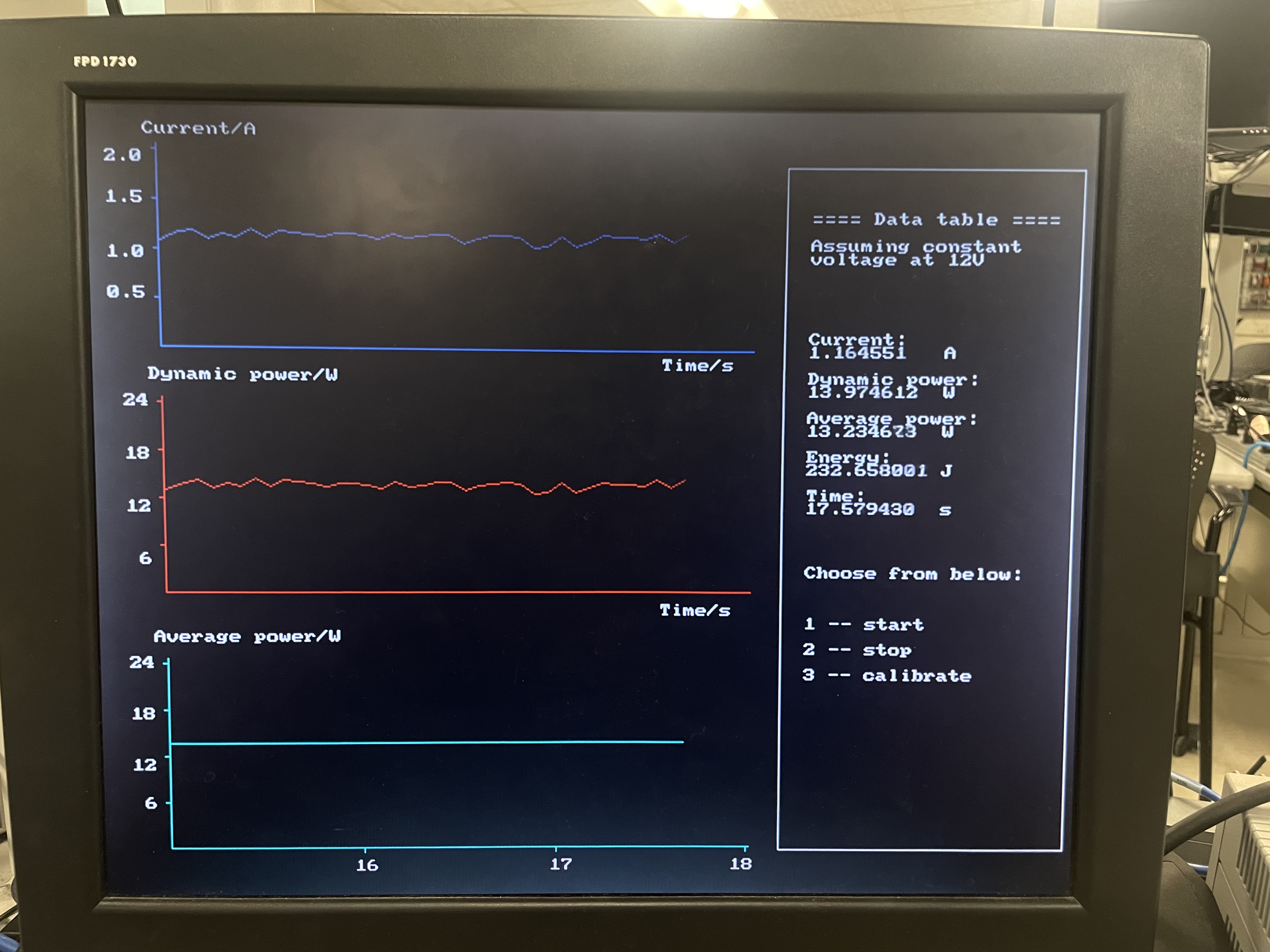
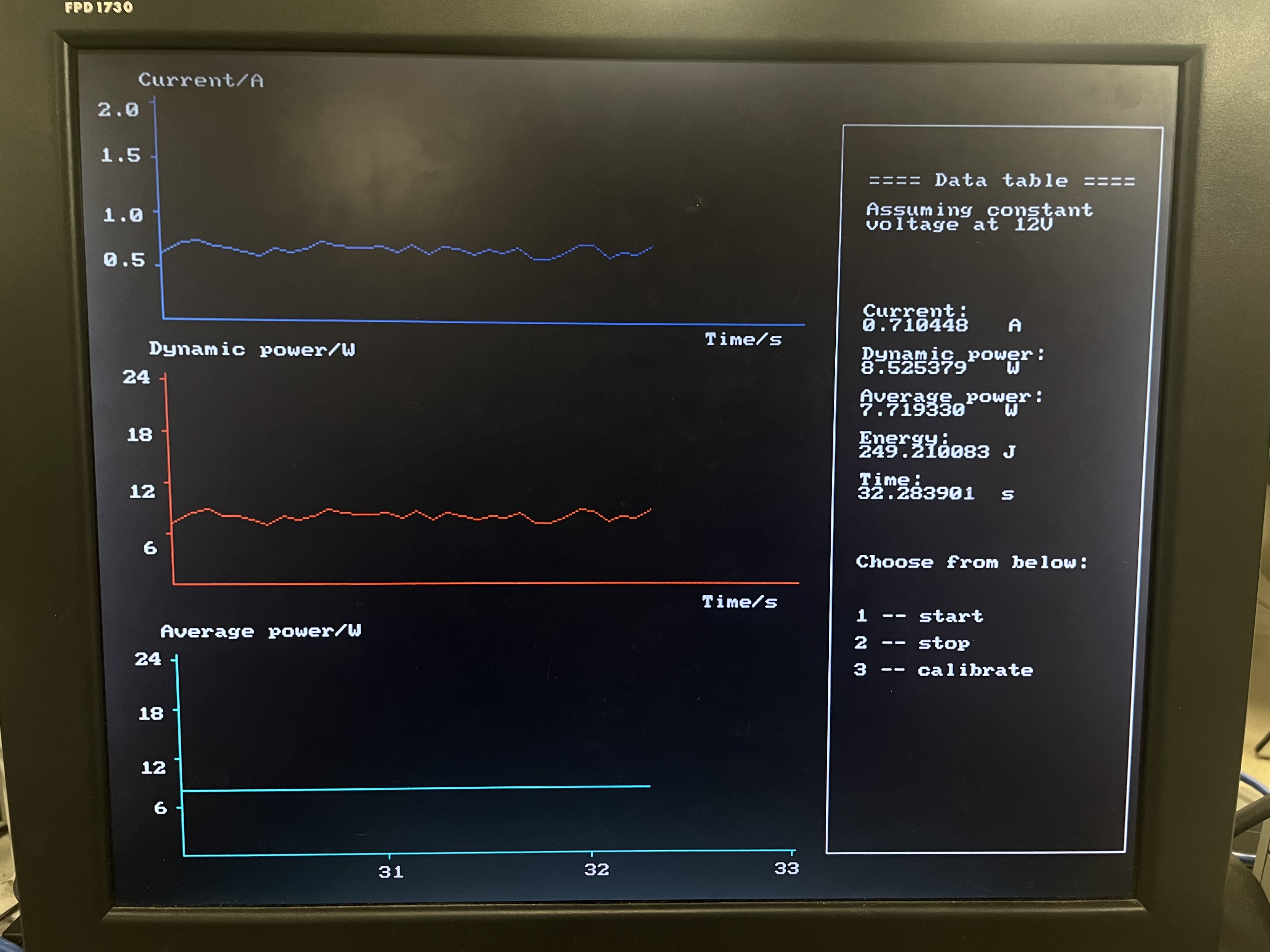
When the system was further verified as above, we were able to use it to explore some interesting power consumption behavior in FPGA. According to some discussion we found in Intel Community, ethernet calble can cause a large amount of enrgy. Our system can be a good choice to demeonstrate whether it is true. So, we chose to use serial to control the FPGA. We first ran the power estimator with the ethernet cable plugged in. The average power in this scenario is around 7.72W as shown in Figure 8. We then disconnected the ethernet cable and calibrated the readings by asserting the signal from the serial interface. The average power immediately drops down to 6.24W as shown in Figure 9. We repeated this process several times to confirm our finding, and we were always able to see a near 1W drop in average power every time we disconnect the ethernet cable. We are, therefore, able to conclude the use of ethernet connection in working with the FPGA increases power consumption significantly. We also tried adding two thousand 32-bit counters in the FPGA to see how power consumption changes, but the change in power consumption was hard to observe.

Conclusion and future development
By the end of this project, we were able build the power estimator close to what we planned at the start. This piece of hardware can act as a standalone ammeter and power estimator, and it may as well be integrated into other projects to help people learn about the power consumption and efficiency of their own system. For most of the labs, we focused on building accelerators for fast computations and synthesis, and while better performance is always preferred, we thought it would be very meaningful to study the corresponding cost in power. Unfortunately, with the limitation of time, we were not able to carry out more investigations, but we believe there is plenty of potential for further testing and improvement. The most direct one is to use this estimator to estimate power consumption of labs we did this semester. For example, lab 3 implementation already used up most of the hardware on the FPGA, we expected more energy and power will be consumed. Also, for example, experiment with adding and removing the VGA and audio subsystem and observing how that affects power consumption can be quite interesting. However, this system also has several flaws. We always consider supply voltage as stable, which is too ideal. There will be inevitable fluctuating in voltage while operating. To further estimate power, we suggest using the internal ADC on DE1 SoC to measure the supply voltage instead of simply assuming it as 12V. Additionally, 110mV/A sensitivity might not be precise enough, we recommended MIKROE-3443 which is also an I2C-based current sensor but with 400mV/A sensitivity.
We referenced the C code example on the ECE5760 course website for assigning addresses to pointers for PIO ports and mapping from physical to virtual address. We also adopted the Quartus project code from the website and instantiated our own modules inside. All datasheets and schematics referenced in this project are public information on internet and is meant for sharing with the general public.
Final demo video
Appendix A
The group approves this report for inclusion on the course website. The group approves the video for inclusion on the course youtube channel.