FPGA-Based Multi-Core Rivest Cipher 4
ECE5760 Spring 2024
Ruyi Zhou (rz443) | Hengyu Wang (hw768) | Bolong Tan (bt362)
Introduction
With the rapid development of digital technologies, cybersecurity has become increasingly crucial. Rivest Cipher 4, or RC4, gained prominence as a stream cipher in the 1990s. This project aims to explore RC4's significance by designing and implementing an encryption and decryption circuit using a modular finite state machines (FSM) approach. It serves as an in-depth study of digital system design and investigates RC4's role in internet communication encryption. The alogirthm is implemented on the DE1-SoC FGPA board. The user interface features slider switches for the secret key, HEX displays for decryption monitoring, and LEDs for key status indication. Functionally, the system initializes and shuffles the S array based on the secret key, performs encryption and decryption using RC4, and includes a brute-force mechanism to demonstrate algorithm vulnerabilities, highlighting the need for robust encryption methods.
High Level Design
-Principle
RC4 algorithm possesses significant advantages due to its dynamic and real-time nature, ensuring consistent encryption and decryption between parties. Its simplicity and fast computation make it a preferred choice for encryption in protocols like HTTPS/SSL. However, recent disclosures suggest potential security risks associated with the algorithm. In traditional implementations, RC4 typically employs a 256-byte key length. The RC4 algorithm generates an array of bytes (S array), with each byte being XOR'ed with a message byte for message decoding. The user inputs a secret key, which affects the state of the S array generated by the algorithm.
The following is the basic procedures of the implementation of RC4 algorithm.
- Initilization the S-array
- -Encryption/Decryption
1.Initialize the S-array by filling the number 0 to 255 to address 0 to 255.
2.Shuffle the order of the S-array using the user-input secret key.
1.For each segment of data to encrypt/decrypt:
-Take the first byte of the key as an index and retrieve the corresponding byte value from the key.
-Preserve this byte as N and swap these two bytes in the key.
2.Calculate the sum of these two bytes.
3.Retrieve one byte from the data to encrypt/decrypt.
4.XOR the two bytes obtained in steps 2 and 3 to achieve encryption/decryption.
5.Take the second byte of the key, add it to byte N as an index.
6.repeat the above steps until the traversal all the elements.
-Algorithm
The following procedures are the algorithm implementation in language C [1].
- Initilization
Initialize the S-array by writing 0 to 255 to address 0 to 255.
                      for(int i = 0; i <= 255; i++){
                        s_array[i] = i;
                      }
Shuffle the S-array according to the user-inputted secret key.
                      int j = 0;
                      int i;
                      int temp_1;

                      for(i = 0; i <= 255; i++){
                        j = (j + s_array[i] + secret_key[i % 3]) % 256;

                        //swap s_array[i] with s_array[j]
                        temp_1 = s_array[i];
                        s_array[i] = s_array[j];
                        s_array[j] = temp_1;
                      }
In our design, the secret key is 24 bits. We divided it into 3 pieces, each piece contains 8 bits. For exmaple, if the secret key is 24'b10101010_11111111_00000000, the secret_key[0] is 8'b00000000, secret_key[1] is 8'b11111111, secret_key[2] is 8'b10101010. In addition, in our HDL design, the variable j is 8-bit long, thus the % 256 can be ignored since when j reaches 255, it will automatically overflow, which has the same effect as % 256.
Since RC4 is a symmetrical algorithm, this means that if we apply the algorithm to a message, it will encrypt it, and if we apply the same algorithm to an encrypted message, it will decrypt it. Thus, both encryption and decryption use exactly the same algorithm. The algorithm is below:
                      int i = 0;
                      int j = 0;
                      int k;
                      int temp_2;
                      int sum;
                      int factor;

                      //loop ends until reaching the message length
                      //In our design each message is 32 bytes long

                      for(k = 0; k <= 31; k++){
                        i = (i + 1) % 256;
                        j = (j + secret_key[i]) % 256

                        //swap s_array[i] with s_array[j]
                        temp_2 = s_array[i];
                        s_array[i] = s_array[j];
                        s_array[j] = temp_2;

                        //get the XOR factor
                        sum = s_array[i] + s_array[j];
                        factor = secret_key[sum % 256];

                        //write to the output using 8 bit-wise XOR
                        RAM[k] = factor ^ ROM[k];
                      }
The RAM is the memory that stores the resulting message, while the ROM contains the message that will be encrypted or decrypted.
-Structure
The following figure represents the hardward sturcture of the project.
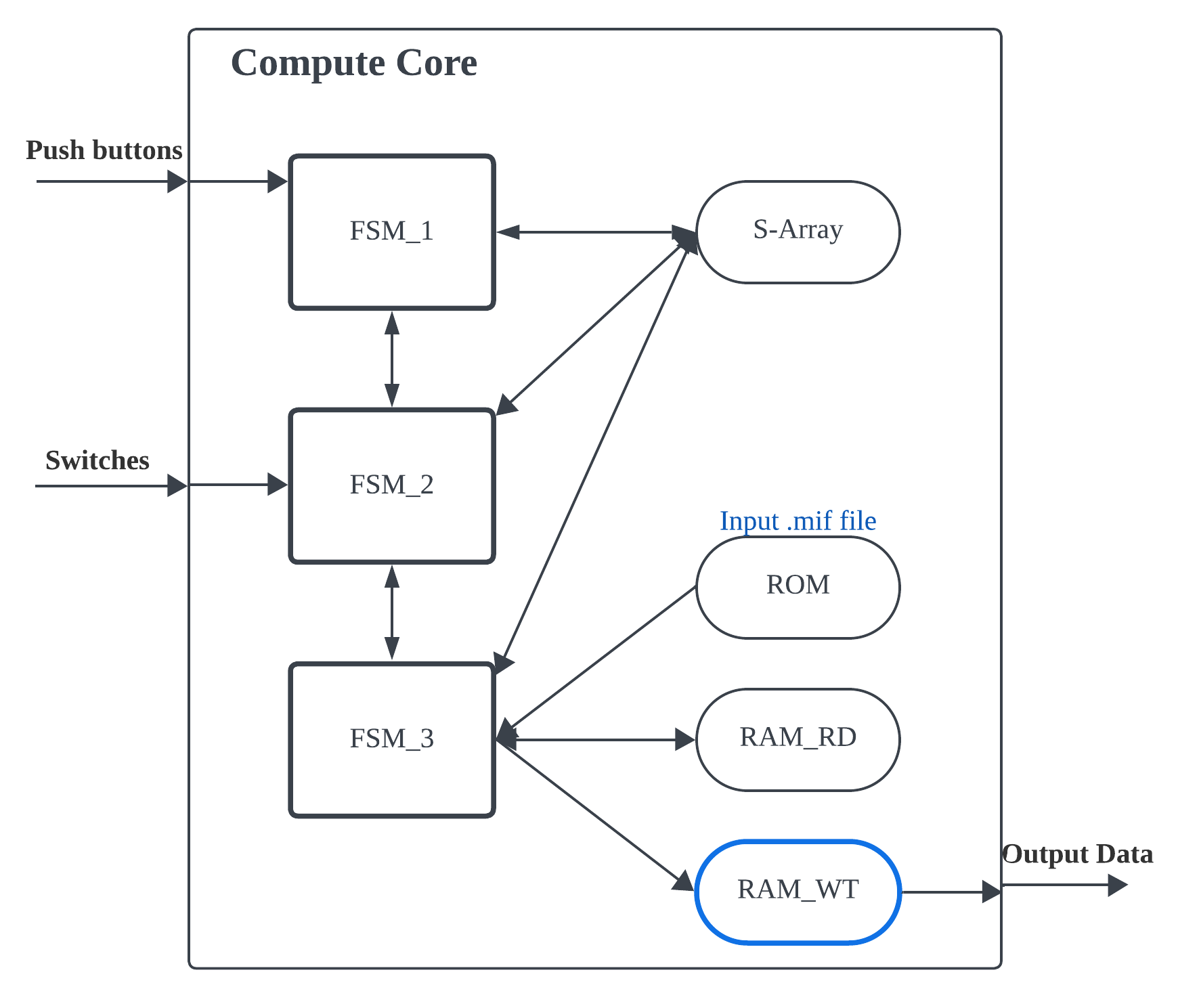
Figure 1. The sturcture of a single core.
As depicted in Figure 1, FSM_1 handles the initialization function, FSM_2 is responsible for shuffling, and FSM_3 is capable of encrypting or decrypting the message character by character. The computation core takes input from the switches and the push button status on DE1-SoC and outputs the successfully decrypted message. Each computation core is equipped with three finite state machines (FSMs) and four memories. The S-Array is an 8x256 memory, signifying that it comprises 256 elements, each of which is 8 bits. The RAMs and ROM are 8x32, indicating that each of them contains 32 8-bit elements. The S-Array RAM is utilized for storing S-array data, while the ROM stores the user's message intended for encryption and decryption. RAM_RD stores the encrypted message, and RAM_WT stores the decrypted message. Additionally, FSM_1 initializes the S-array. Following completion of FSM_1, FSM_2 proceeds to shuffle the S-array based on the switches, effectively the user-inputted secret key. After shuffling, pressing KEY_1 triggers FSM_3 to retrieve data from the ROM and apply the encryption algorithm. Subsequently, it writes the encrypted data into the RAM_RD memory. Subsequently, pressing KEY_0 initiates FSM_1, FSM_2, and FSM_3 to repeat the above procedures for decrypting the message. The difference lies in FSM retrieving data from RAM_RD (the encrypted message) instead of the ROM. It t hen writes the decrypted message into the RAM_WT memory and outputs it to the top-level module. Additionally, the HEX displays on the DE1-SoC indicate the operation time in terms of clock cycles.
Additionally, the design possesses the capability to brute-force crack the cipher. The secret key consists of 24 bits. Due to the constraints of the switches on DE1-SoC, SW9 represents the 24th bit of the secret key, while SW8 to SW0 are connected to secret_key[8:0]. All other bits are hardwired to 0s. When the user presses KEY_2, the design initiates the brute-force cracking of the secret key. To crack the secret key, the procedures remain identical to those outlined previously. The FSMs no longer utilize the switches as the secret key; instead, they iterate through keys from 24'b00..00 to 24'b11..11, applying the algorithm for each key until the correct key is found. As the message is encoded using ASCII code, the design examines the decrypted data individually. If the data falls within the range of letters or numbers in ASCII code, it is flagged as correct. When all 32 data items in the memory are flagged as correct, the current secret key is considered the correct key.
-Top-Level Module
The brute-force cracking procedure iterates through all 16,777,216 secret keys from 24'b00...00 to 24'b11...11. This process takes approximately 5 hours to complete. Therefore, we implement 16 computation cores to simultaneously traverse the secret keys in parallel during the cracking process. The top-level structure is as follows:
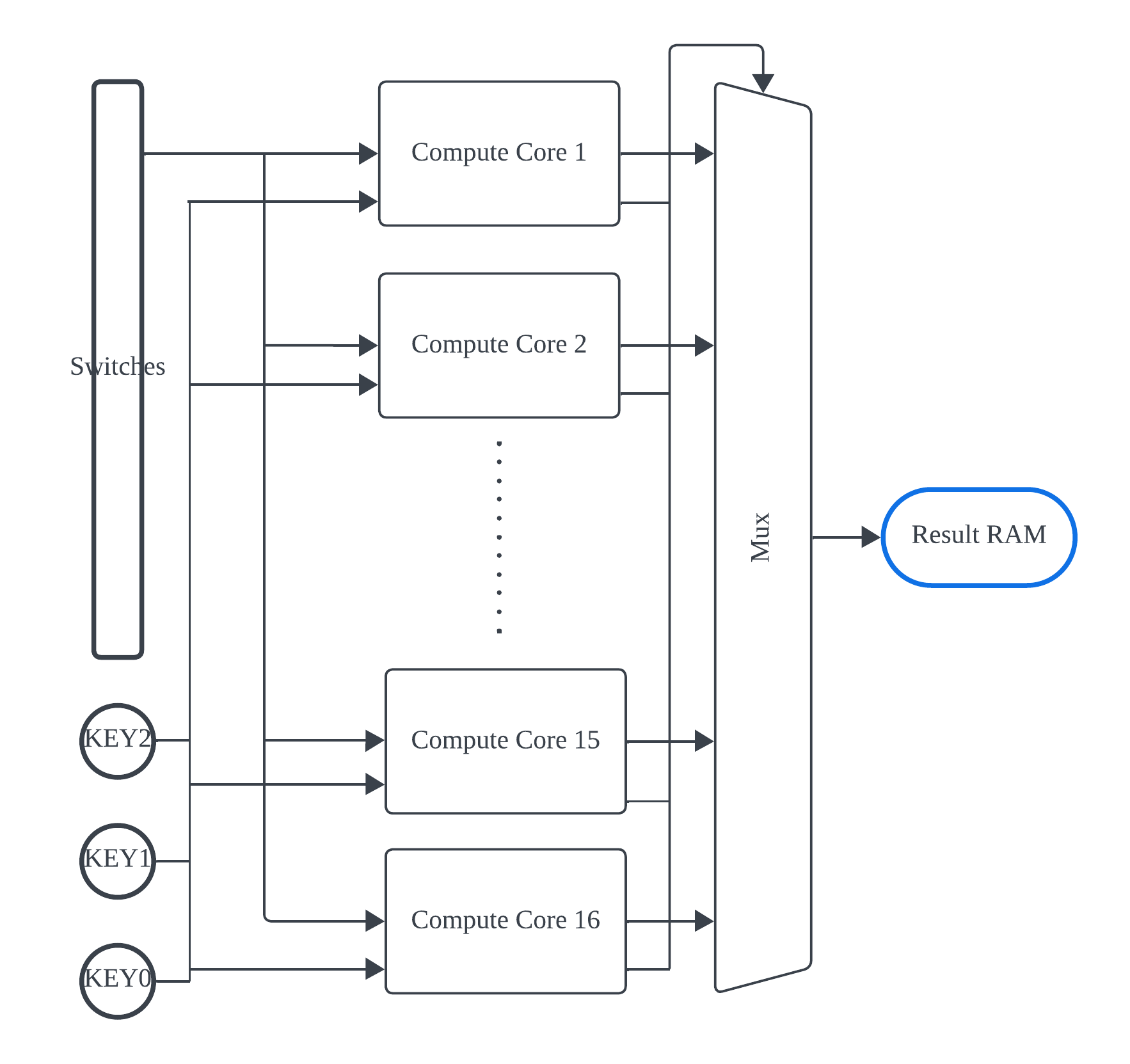
Figure 2. The sturcture of top-level design.
As illustrated in Figure 2, each compute core receives inputs from the switches and push buttons and applies the algorithm to the memories within each core. The principle behind this multi-core design is that we divide the secret key range (from 24'b00..00 to 24'b11..11) into 16 segments. Each individual core computes the secret keys within a specific range. This design significantly reduces computation time due to parallel computation. Ideally, this multi-core design can achieve a 16-fold speedup in terms of clock cycles. The actual speedup is discussed in the Results section. The 16 cores simultaneously process different secret keys and output 16 decrypted messages at the same time. However, only one core identifies the correct key. When a core flags 32 correct data entries, it outputs a correct signal, which serves as the select signal in the multiplexer. The message from the correct core is then written into the result RAM.
Hardware Design
-Finite State Machines
The core focus of this project revolves around the three finite state machines (FSMs) and the interfaces between them. The designs are simulated in ModelSim and synthesized in Quartus 18.1. The flowcharts below illustrate the principles governing each FSM.
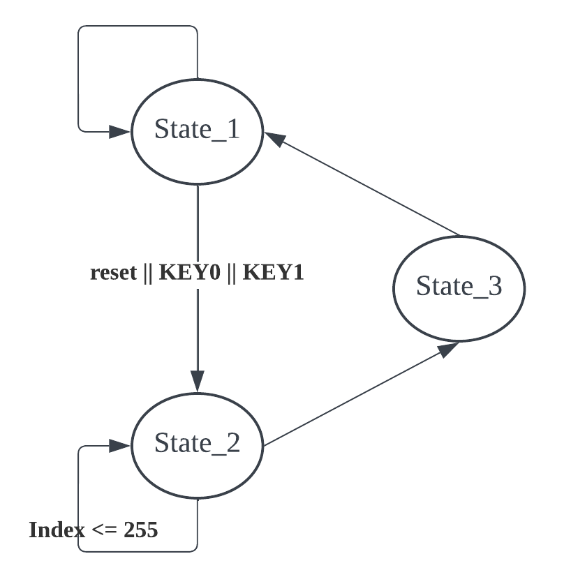
Figure 3. The flowchart of the 1st FSM.
This FSM achieves the function of the initilization part of the algorithm. The purpose and function of each state are illustrated below:
Table 1. The states functions of the 1st FSM.
| States | Functions | Outputs |
| state_1 | Waiting for the reset or start signal | Computation start signal |
| state_2 | Fill up the S-array memory with 0-255 | NONE |
| state_3 | Reset all the registers | Finish signal |
When the first FSM completes its operation, it sends a finish signal to the second FSM. Subsequently, the second FSM initiates the shuffling process of the S-array based on the user-inputted secret key. The states (other than check state) in this FSM proceed sequentially as the clock changes, as this FSM represents the hardware implementation of the algorithm.The following figure and table illustrate the principle of the second FSM.
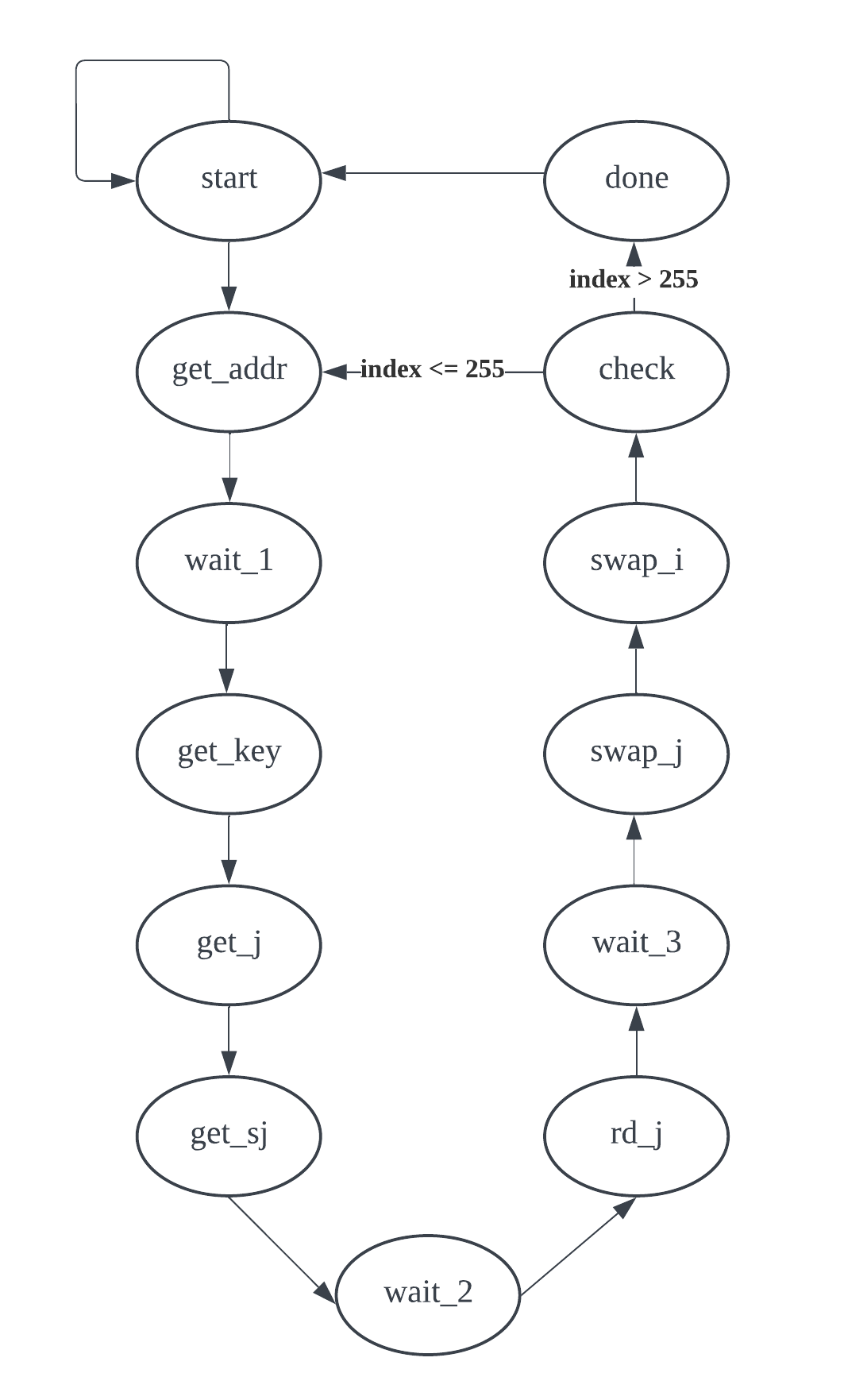
Figure 4. The flowchart of the 2nd FSM.
Table 2. The states functions of the 2nd FSM.
| States | Functions | Outputs |
| start | Wait for start signal from FSM_1 | NONE |
| get_addr | Request the index i for S_array | NONE |
| wait_1 | Wait one cycle for memory reading | NONE |
| get_key | Get the designed secret_key piece | NONE |
| get_j | Calculate the index j for S_array | NONE |
| get_sj | Request the s_array[j] value | NONE |
| wait_2 | Wait one cycle for memory reading | NONE |
| rd_j | Receive the s_array[j] value from memory | NONE |
| wait_3 | Wait one cycle for memory reading | NONE |
| swap_j | Write s_array[j] data to s_array[i] | write enable |
| swap_i | Write s_array[i] data to s_array[j] | write enable |
| check | Check if traversal the entire S-array memory | NONE |
| done | Finish the shuffling | Start decrypting signal |
As depicted in Figure 4 and Table 2, FSM_2 serves as the hardware implementation for shuffling in the algorithm. The states proceed sequentially to shuffle the elements in the S-array according to the user-input secret key. At the check state, the FSM verifies if it has traversed all elements in the S-array. If not, it updates the index "i" by incrementing it by one and returns to the get_addr state to repeat the process until the index "i" reaches 255. Upon reaching the done state, the FSM emits a start_decryption signal, triggering the third FSM.
The following figure and table represnt the principle of the third FSM, which implements the encryption or decryption part of the algorithm.
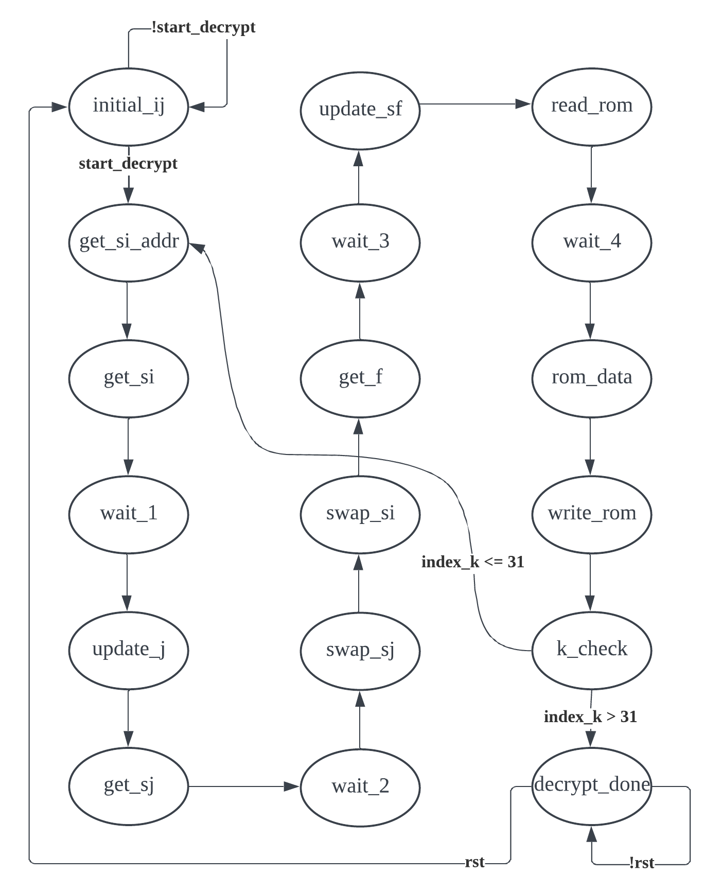
Figure 5. The flowchart of the 3rd FSM.
Table 3. The states functions of the 3rd FSM.
| States | Functions | Outputs |
| initial_ij | Initialize index i,j to 0 and wait for trigger signal | NONE |
| get_si_addr | Update index i | NONE |
| get_si | Request the s_array[i] value | NONE |
| wait_1 | Wait one cycle for memory reading | NONE |
| update_j | Receive s_array[i] and update index j | NONE |
| get_sj | Request the s_array[j] value | NONE |
| wait_2 | Wait one cycle for memory reading | NONE |
| swap_sj | Receive s_array[j] value and put it to s_array[i] | write enable |
| swap_si | Put s_array[i] value to s_array[j] | write enable |
| get_f | Request the secret_key piece to compute the f factor | NONE |
| wait_3 | Wait one cycle for memory reading | NONE |
| update_sf | Receive the secret_key piece and get the f factor | NONE |
| read_rom | Request the data in the ROM | NONE |
| wait_4 | Wait one cycle for memory reading | NONE |
| rom_data | Receive the data from ROM and XOR with factor to encrypt/decrypt | NONE |
| write_ram | Write the encrypted/decrypted data to the RAM | ram write enable |
| k_check | Check if travesal all the elements in the memory | NONE |
| decryption_done | Finish encryption/decryption | Done signal |
The same as FSM_2, FSM_3 is also a sequentially-proceeding state machine as it implements the encryption/decryption part of the algorithm (as mentioned before, the process is exactly the same). In Figure 5, FSM_3 is initially at initial_ij state to initialize index i and j to 0 and waits for the trigger signal from FSM_2. Upon receiving the trigger signal, it proceeds through the following states: calculating the index i by incrementing 1, calculating index j by adding the secret key piece. Then it goes through the swap states to interchange the values of s_array[i] and s_array[j]. After swapping, the FSM sums them up and utilizes this result to obtain the desired secret key piece (8 bits of the 24 bits). This result is referred to as factor. Then the factor is XORed with the message from the ROM to encrypt/decrypt the message. The result is then written into the result RAM.
-Brute-Force Cracking and Multiple Cores
Our design also incorporates the brute-force cracking function. Initially, the readable .mif file is manually inputted into the ROM. Then, the user sets up a secret key using the switches and presses KEY1 to encrypt it. Normally, the encrypted message can be decrypted using the SAME secret key by pressing KEY0. However, if the user forgets the secret key, he or she can press KEY3 to brute-force crack the cipher. The principle is that the FSMs mentioned above will proceed through the same procedures. The difference lies in the cracking mode, where the FSMs do not take switches as user-input secret keys. Instead, they traverse the secret key from 24'b00..00 to 24'b11..11. Thus, when KEY3 is pressed, the circuit generates a cracking signal, which also resets the first FSM to re-do the process. Additionally, when at the write_ram state in the third FSM, the FSM checks the correctness of the decrypted message by verifying if the decrypted data falls within the ASCII range. If all 32 decrypted data are within the ASCII range, the current secret key is correct, and we obtain the correct message.
Additionally, traversing from 24'b00..00 to 24'b11..11 results in 16,777,216 secret keys, a process that takes about 5 hours. Therefore, we implement sixteen cores, with each core responsible for a specific range of the secret key since the range is equally divided into 16 pieces. The message from the correct core will be written into the result RAM. This significantly reduces the operation time by sixteen times.
-Timing
To calculate the time of each computation, we incorporate a common timer inside each FSM. In each state, the timer increments by one. Therefore, at the last state of FSM_3, the timer reflects the total clock cycles used by the entire process. This number is sent to the top-level and displayed on the HEX displays on the DE1-SoC board.
In addition, in the cracking mode, we have sixteen cores, and each core has its own timer. This is redundant since each core operates in parallel, so the timers are exactly the same. Another consideration is that, in brute-force cracking mode, each core will traverse multiple secret keys, resulting in a large timer count that may exceed the six HEX displays capacity. Therefore, in this mode, the timer will only increment by one when it finishes one secret key traversal. Thus, the timer in this mode reflects the number of traversals. The operation time can be obtained by multiplying the number of traversals by the number of clock cycles for one traversal.
Results of Design
According to the demonstration procedures, the first step is to load the .mif file containing the message into the ROM. The figure below shows the loaded ROM.
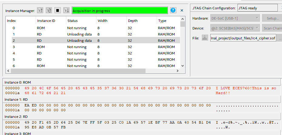
Figure 6. The ROM after loading the message.
As depicted in Figure 6, after loading the message into the ROM, the In-Content Memory Editor in Quartus 18.1 displays the correct message in the ROM, which is I LOVE ECE5760! This is so Hard!!. Then, after the user presses KEY1 to encrypt it, the RAM displays the encrypted message as follows:
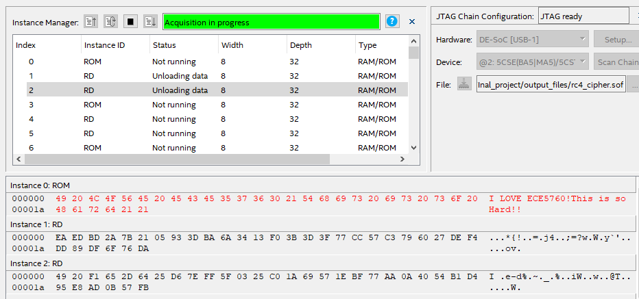
Figure 7. The RAM after encrypting the message.
The RAM named "Instance 1 RD" contains the encrypted message. The RAM named "Instance 2 RD" is used to store the decrypted message when the user presses KEY0. Upon pressing KEY0, the FSMs begin decrypting the message and write the results into "Instant 2" RAM as follows:
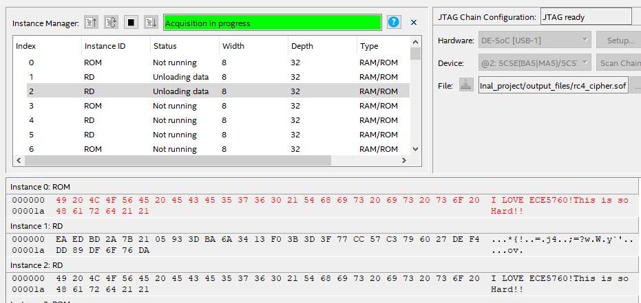
Figure 8. The RAM after decrypting the message.
It can be observed that the decrypted message is written into the result RAM, and it exactly matches the original message. This indicates that the functionality of our design is as expected. The figure below displays the number of clock cycles used for one traversal computation time, which is E02 cycles (in hexadecimal).
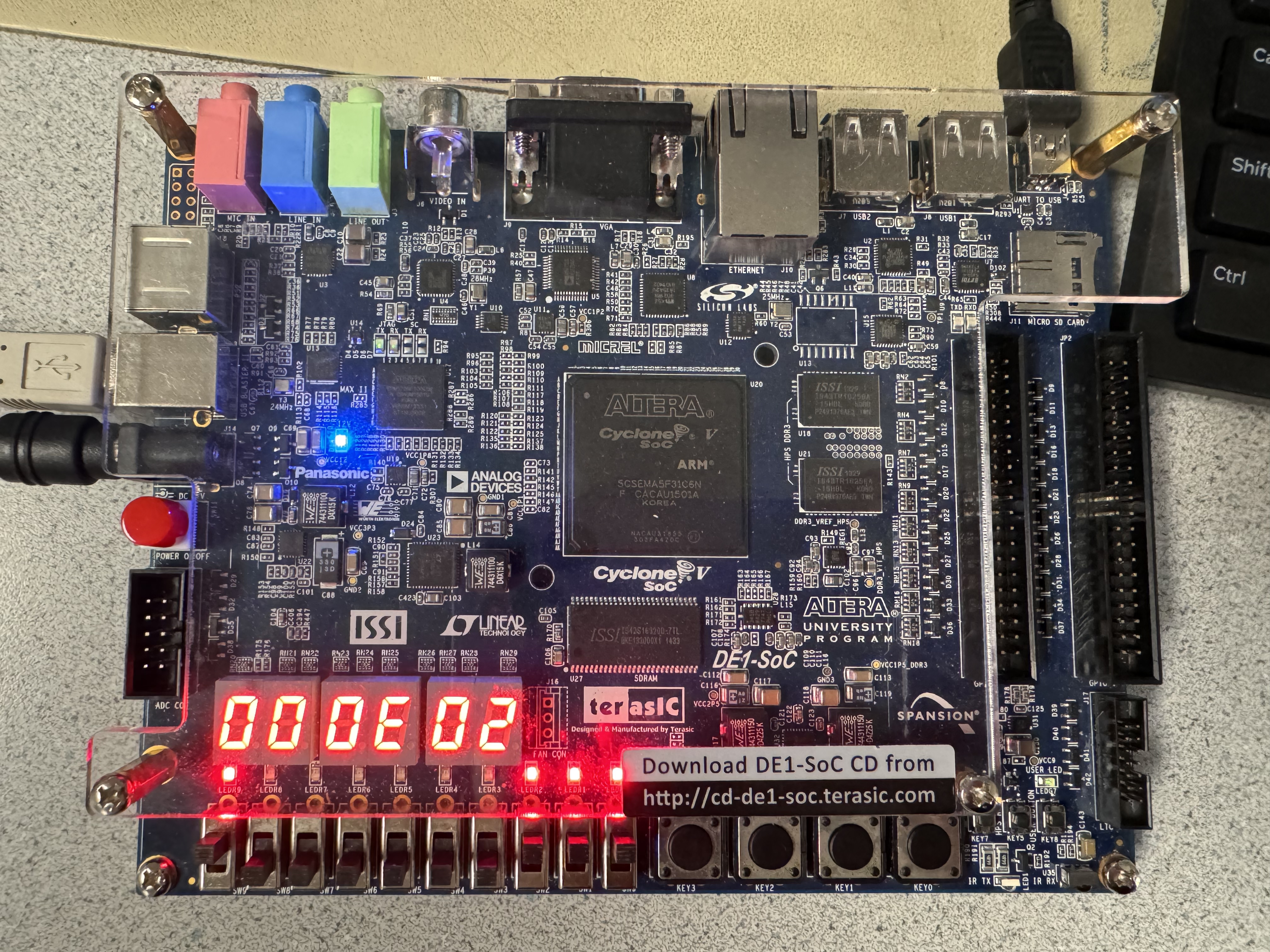
Figure 9. The computation time for one traversal.
Additionally, the multi-core design comprises sixteen cores, with each core containing one ROM and two RAMs, resulting in a total of 48 memories for the cores (instances 0 - 47). The final correct result RAM for the multi-core outputs is implemented in the top-level module. Upon the user pressing KEY3 to brute-force crack the cipher, the correct message is written into the result RAM (instance 48) in the top-level module as depicted below:

Figure 10. The result RAM for multi-core output.
To test the worst-case scenario, we hardwired the correct secret key to 24'b11..111. With one core, the number of traversals will be 16,777,216. We decrypted it using the multi-core design. Subsequently, the HEX display on the DE1-SoC shows a number of 0xFFFFF (1,048,576 in decimal). This number is one sixteenth of 16,777,216. This indicates that our multi-core functionality works well and achieves a sixteen times speedup in terms of computation time.
Conclusions
In conclusion, the RC4 software algorithm utilized in this project is sourced from open access. We have explored the significance of RC4 within the cybersecurity landscape, particularly amidst the rapid evolution of digital technologies. Through the implementation of an encryption and decryption circuit using a modular FSM approach on the DE1-SoC FPGA board, we delved into RC4's role in communication encryption. The memories used in our design are IP cores generated from the Altera IP Catalog. Leveraging features such as slider switches for the secret key and LEDs for key status indication, our system showcased seamless encryption and decryption processes while highlighting algorithm vulnerabilities through a brute-force mechanism. Notably, our multi-core design achieved a remarkable sixteen-fold acceleration under worst-case scenarios, emphasizing the efficiency and efficacy of our approach. These findings advocate for ongoing innovation in encryption methodologies to bolster data protection in an ever-evolving digital landscape. Additionally, resources on the DE1-SoC remain available. Therefore, more computation cores may be added to our design, but the increased complexity is balanced against hardware resource limitations and critical path considerations, which affect the timing requirements on the FPGA. Hence, future development and consideration are still needed.
Demonstration Video
References
[1] Zhihu. "Study Notes on 'Computer Networks'" [Online]. Available: https://zhuanlan.zhihu.com/p/537881813
[2] Mouser Electronics. "DE1-SoC User Manual" [Online]. Available: https://www.mouser.com/datasheet/2/598/DE1-SoC_User_manual_v06-1214842.pdf
[3] The html template from Professor Joe Skovira.
Appendix A
The group approves this report for inclusion on the course website.
The group approves the video for inclusion on the course youtube channel.
Appendix B
This appendix contains the verilog source codes and other necessary files we used in this project.
The top-level module:
rc4_cipher_top.v
The 1-Port S-array RAM of Altera IP Core:
s_array.v
The 1-Port ROM of Altera IP Core:
encrypted_msg.v
The 1-Port results RAM of Altera IP Core:
decrypted_msg.v
The .mif file created by ourself to be loaded to the ROM:
original_msg.mif
The SRAM Object File (.sof) that programs the FPGA:
rc4_cipher.sof