Project Introduction
Our project involves implementing a 5-stage pipeline processor that supports the RISC-V instruction set on the DE1-SoC. We modified the processor code from ECE 5740 to make it synthesizable and developed a memory system and interface for interaction with the processor. We also created a source module for initializing the register file and a sink module for verifying register values. These components form the hardware implementation on the FPGA. On the HPS side, we designed an interactive interface to initialize memory and source according to an assembly program, control the processor's operation, and display a line trace for performance monitoring. Additionally, we created a VGA display to visually demonstrate sorting algorithms using color changes.
High level design
Rationale and sources of our project idea
Inspired by the ECE 5740 Computer Architecture course, we decided to implement a complex processor system on the DE1-SoC. This serves two purposes: first, it allows us to review and verify the knowledge we previously acquired. In ECE 5740 Lab 2, we designed a 5-stage pipeline processor based on RISC-V that can execute a subset of RISC-V instructions. At that time, we only simulated the design and did not run the hardware code as synthesizable hardware. Second, considering that processors are ubiquitous in our daily lives, from smartphones to computers, we believe running programs we wrote on a processor we built ourselves is really cool.
Logical structure
Our project involves implementing a 5-stage pipeline processor that supports the RISC-V instruction set on the DE1-SoC. Our high-level design structure is shown in figure 1.
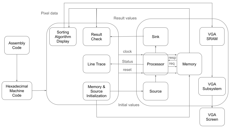
Figure 1. High Level Design Structure
We modified the processor code from ECE 5740 to make it synthesizable. We then developed a memory system that interacts with the processor, including the memory itself and its interface with the processor. Additionally, we created a source module for initializing the processor's register file and a sink module for verifying the values in specific registers for testing purposes. These components constitute the hardware implementation on the FPGA.
On the HPS side, we designed an interactive interface for the processor. This interface initializes the memory and source according to a specified assembly program, loads instructions and data into designated locations, and controls the processor's operation through clock and reset signals. A line trace feature displays detailed information about the processor's operation, allowing us to monitor its performance and ensure it runs correctly. Finally, the interface shows the memory content after execution to verify correctness and receives the detection results from the sink module.
To provide a better visual experience and more intuitively display the processor's results, we created a VGA display that uses color changes to demonstrate sorting algorithms.
Hardware/software trade offs
For the hardware part, it is almost only responsible for running the processor to execute instructions. Our processor execution process is pipelined, therefore running it on FPGA is intuitive and efficient due to its large parallel computing resource. The initialization of memory is relatively a redundant process for FPGA, so we choose to use the shared M10K which allows access from both ARM and FPGA side so that we can easily initialize the instruction, data and source memory from ARM. And it is also convenient for ARM to open and read the hex file, which contains machine code, that was converted from the assembly program. Besides, we decided to control the VGA from the ARM side, which is more convenient to build fancy demonstrations. By handling all these steps in the software section on the ARM side for display and initialization, we can save a significant amount of time during the project development process. This allows us to focus on the implementation of the processor.
Existing patents, copyrights, and trademarks relevant to this project
This project is based on the open-source RISC-V instruction set and incorporates parts of the code from ECE 5740 lab 2. Therefore, we believe this project does not entirely belong to us.
Hardware design
Processor
The structure of our implemented processor is largely based on Lab 2 of ECE 5740 Computer Architecture. This lab involves a five-stage processor pipeline that uses stalling and squashing to resolve hazards and employs bypassing to enhance processor performance. Specifically, this processor comprises five stages: fetch, decode, execute, memory, and write. These stages operate concurrently, allowing up to five instructions to be processed simultaneously within the processor. Briefly, the fetch stage is responsible for retrieving the next required instruction from memory. The decode stage analyzes the fetched instruction to determine its type, the source and destination registers involved, the use of immediate values, and the specific operation to execute, including extracting data from the register file. The execute stage performs the necessary computations, the memory stage handles interactions with memory (reading or writing), and finally, the write stage stores the resulting data in the target register.
The processor supports the RISC-V instruction set architecture (ISA), more specifically the Tiny RISC-V ISA subset, which includes all instructions except those related to system calls. The list of instructions that constitute TinyRV2 is shown in figure 2. There are six categories of instructions: Register-Register Arithmetic Instructions, Register-Immediate Arithmetic Instructions, Memory Instructions, Unconditional Jump Instructions, Conditional Branch Instructions, and Control/Status Register Instructions. After implementing all TinyRV2 instructions, our processor is capable of executing simple C programs that do not use system calls.
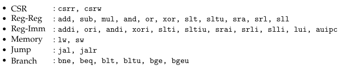
Figure 2. TinyRV2 instructions
The processor consists of two main parts: the datapath and the control unit. The datapath is the hardware that performs all the required operations, such as the ALU, registers, and internal buses. Its specific structure is shown in figure 3. The control unit is the hardware that directs the datapath in terms of switching, operation selection, and data movement between ALU components. The blue and orange arrows in figure 3 represent the control signals sent from the control unit to the datapath. The black arrows are signals from or to memory/source/sink. Finally, a higher-level module combines the two parts to form a complete processor. The red paths represent the routes taken by the bypassed data.
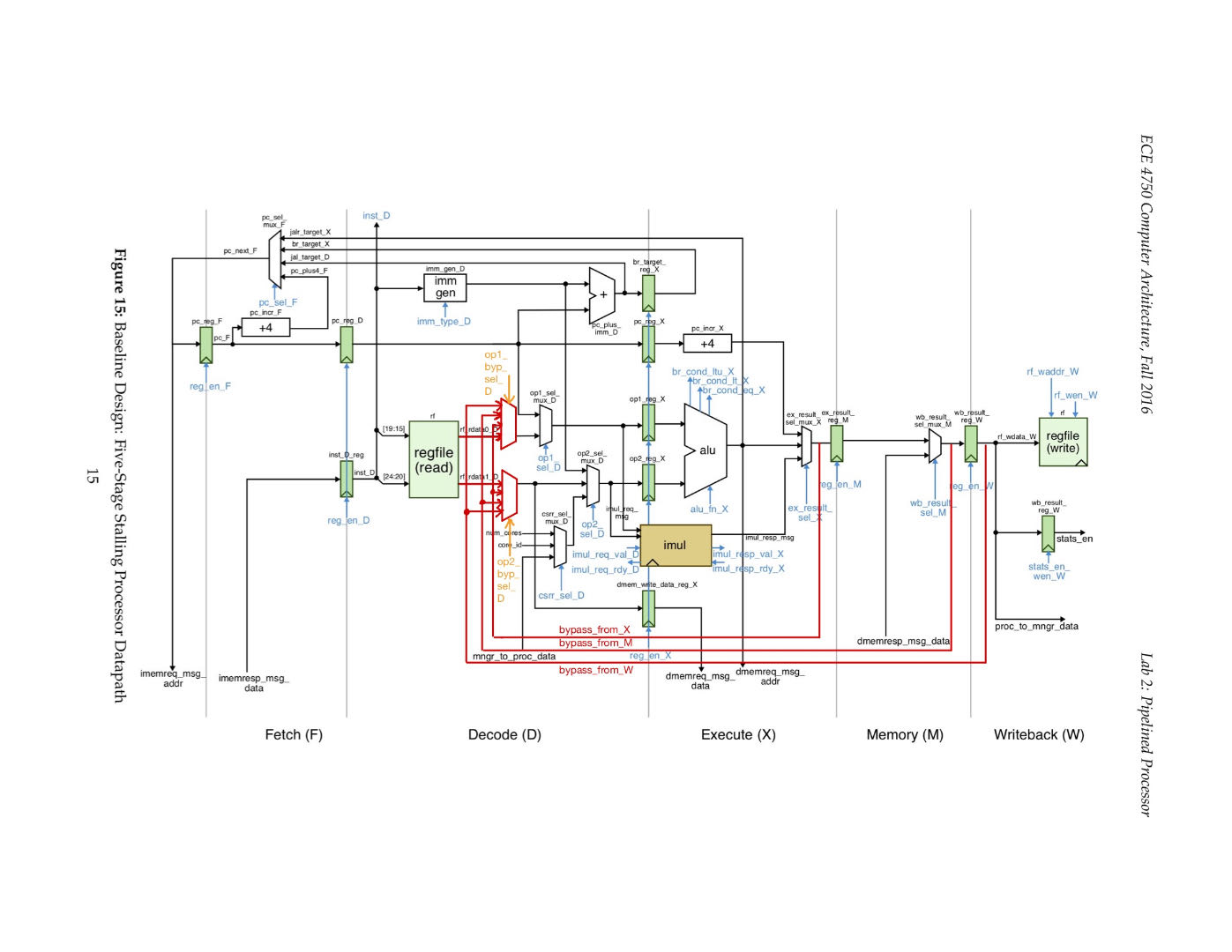
Figure 3. Datapath of processor
Our work primarily involved making the code from ECE 5740 Lab 2 synthesizable. The original code contained some unsynthesizable parts, intended for testing and simulation purposes. To enable the processor to run smoothly on an FPGA, we made several modifications and deletions. Specifically, we removed the line trace display parts used in the testing environment and adjusted some signal types and module interfaces. For more details, please refer to the ECE 5740 website, where you can find all the introductory information except the specific code. The inspiration for the memory, source, and sink components mentioned later can also be found on this website.
Memory
In ECE 5740 Lab 2, the memory module is a completely unsynthesizable test module. To run our processor properly, we needed to design our own memory system. Our memory system is shown in figure 4. The memory system consists of two main parts: the memory storage method and its interface with the processor.
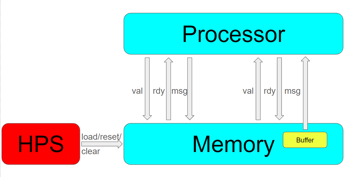
Figure 4. Memory system
For the storage method, we chose to use shared M10K dual-port on-chip SRAM to store the memory data. This configuration supports simultaneous read and write operations and connects to the AXI bus, allowing both the HPS and FPGA to read and write to it. This choice facilitates easier initialization because we plan to use a C program to read the assembly program, making it more straightforward to write data directly into the memory through the HPS. Specifically, since it is a pipelined processor that may perform both instruction and data read/write operations simultaneously, we used two M10K modules, one for instruction memory and one for data memory, each capable of storing 256 32-bit data entries.
The memory interface can be seen in figure 4. The HPS can directly read and write to the configured addresses, enabling initial value loading, resetting, and clearing functions. Compared to processing signals and data on the FPGA, this significantly reduces our workload. The processor on the FPGA and the memory communicate through a valid/ready interface. Specifically, the processor sends a memory request message across a val/rdy interface to the memory, and the memory responds with a message back to the processor one or more cycles later.
In a real-world scenario, the processor and memory are not perfectly synchronized. Various situations can occur: the memory response message might arrive many cycles later, and the memory might not be ready to accept a request. Additionally, the processor may use stalling or squashing to handle hazards, pausing or rolling back its state, which means it cannot send requests or receive responses at those times. To handle these scenarios, we need a latency-insensitive interface, which is our val/ready interface. This works by setting the valid signal high when the sender has a message to send and the ready signal high when the sender can receive a message. When both the valid and ready signals are high in the same cycle, the message is transmitted, and both parties proceed accordingly, ensuring successful message transmission.
Through Qsys module configuration, M10K can support read operations within a single cycle, so when a request val/rdy pair succeeds, the response message data can be read immediately. This way, signal matching and data reading can happen within one cycle, greatly simplifying the processing logic. However, due to the processor's pipeline characteristics, when the processor sends a memory request, it expects to receive the response message at least one cycle later. We need to buffer the information and send it as a response message in subsequent cycles.
Next, I will detail the operations performed within the memory. The specific formats of the memory request and memory response are shown in figure 5. The type indicates whether the message corresponds to a read or write operation. Upon receiving the request, it is unpacked, and based on the type, M10K's write enable is set. The same type is then packed for the response message. The addr in the request represents the target address for the read or write operation. This address is 32 bits, but M10K only has 1024 entries, so we use the lower 10 bits of the address. Additionally, because the processor assumes that all data in memory, including both the instruction and data sections, is stored in contiguous addresses, the data addresses start from 0x2000, and the instruction addresses start from 0x200 due to the processor's assumption of other information stored in memory. However, our two M10K modules use addresses starting from 0, so we subtract 0x200 from the instruction addresses and 0x2000 from the data addresses. Since this address points to each byte and M10K entries are 32 bits each, we further ignore the last two bits to use it as the M10K address. What’s more, due to the fact that the processor assumes Opaque and test are used for simulation purposes and have no practical significance. Len represents the number of bytes of actual data in the message, with 1-3 indicating 1-3 bytes and 0 indicating four bytes. Data contains the data to be transferred, and in the case of a read memory request, the request message's data is invalid, while for a write memory response, the response message's data is invalid.
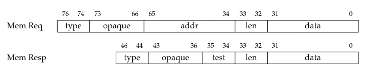
Figure 5. Message format
The memory request rdy signal is set high when the buffer is empty or when the response handshake in the current cycle can send the buffered message. The memory response val signal is set high when there is data in the buffer. When the buffer is empty, it stores the contents upon receiving a request message. When not empty, if the response message is successfully sent, it stores new data or clears based on the request part's situation. If the response message cannot be sent, it retains the existing data.
Source/Sink
The Source and Sink components work in conjunction with the previously mentioned Control/Status Register Instructions. The Source component works with the csrr instruction to store a specific value into a specific register in the register file, typically used to initialize the register file in the processor. The Sink component works with the csrw instruction to send the value from a specific register in the register file to the sink, where it is stored and used to verify if the value at a specific stage matches our expectations, thus checking if the processor is functioning correctly. The communication diagram between the Source, Sink, and Processor is shown in figure 6.
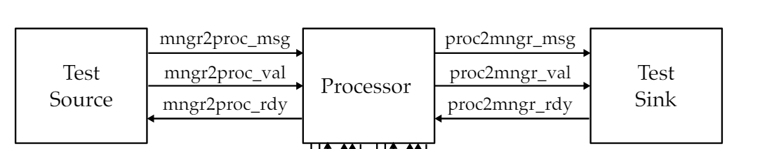
Figure 6. Communication between the Source, Sink, and Processor
The Source and Sink can be viewed as small memory units: the Source only sends information to the processor, and the Sink only receives information from the processor. Therefore, we used a val/rdy interface similar to the one used for memory. Notably, the message here only contains 32-bit data and does not include the type, len, and other parts of the memory message, as the communication only requires the 32-bit value to be stored or retrieved from the register, with other information embedded in the csrr or csrw instructions.
We also used shared M10K dual-port on-chip SRAM, making it easy to initialize the Source and compare the Sink's received data with the expected data from the assembly program. We used two M10Ks, each capable of storing 40 32-bit data entries, as there are typically not many csrr and csrw instructions in actual programs, so large capacity is unnecessary. Additionally, the Source and Sink use an incrementing counter to calculate the address for reading and writing to the M10K, as we are not interested in the content at any specific address; we only need to read or write sequentially. After successfully reading or writing an address, it automatically moves to the next one.
Moreover, after the HPS reads the assembly program, it provides the Source and Sink with a maximum address, indicating that the task is complete once this address is reached. The Source and Sink will then assert the done signal to indicate task completion. The Source keeps the valid signal high at all times except during the reset phase and when the done signal is high. Similarly, the Sink keeps the ready signal high at all times except during the reset phase and when the done signal is high.
Qsys
In the Qsys layout, we connect our board to the VGA subsystem driver which uses SDRAM as the frame buffer for displaying. For instantiating the instruction memory, data memory, memory for sink and memory for source of the processor, we utilize the shared M10K dual port on-chip SRAM which hangs on the AXI bus. The reason why we decided to use it to construct our memory is that it can be easily accessed by both the ARM processor and FPGA side, which makes it easier for memory initialization and extraction.
Besides, we built several PIOs that hang on AXI bus for communication between ARM and FPGA. The PIOs, “arm_reset”, “arm_clk” provided by ARM side are sent to the FPGA as the processor reset and clock signal. As we generate the clock signal from the ARM processor, it is convenient to print out the line trace which shows the status of each stage on the pipeline processor. The “Source_max” and “Sink_max” signal is specified by the specific assembly program, which indicates the number of instructions “csrr” and “csrw” in the program. Some other signals are output from FPGA to ARM for demonstrating the processing procedure and performance of the processor, like the “counter” records the total cycles it spent on running the assembly program, and "done_signal" indicates the completion of the program. The remaining PIOs that start with “info” are used for exposing the required information to the ARM side for linetrace, a more understandable working procedure demonstration.
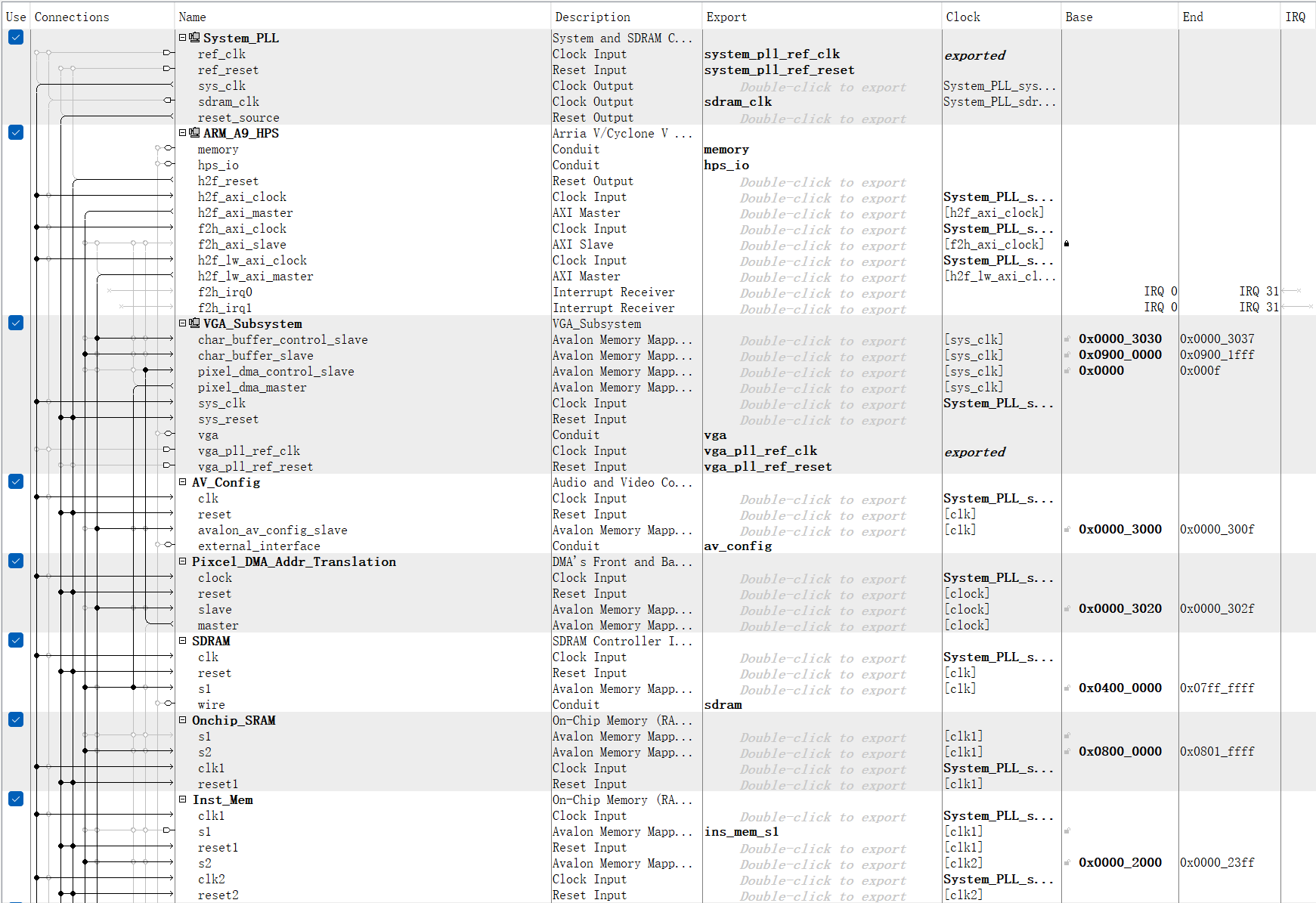

Figure 7. Qsys layout
Program design
C PROGRAM
1. GENERAL
The responsibility of the C program on ARM side includes three parts:
-Initialization of Memories & Content of regfiles and memory verification
-Line Trace demonstration
-VGA Display for showing sorting algorithm
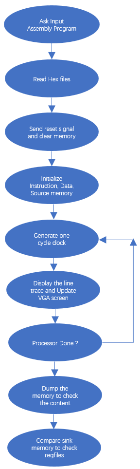
Figure 8. Work flow of C program
Figure 8 demonstrates the work flow of the C program. When running the C program on the ARM side, it will ask for user input to choose the assembly program to execute. It reads the hex files (containing machine code for memory, source and expected value for registers) and sends a reset signal to reset the whole processor system. After clearing the memory, it starts the initialization of instruction memory, data memory and memory for source. Then it starts to provide a constant clock signal to the processor on FPGA through PIOs. Each time when one rising clock edge is issued, it prints out the line trace which includes the status of each stage on the pipelined processor to show the processor’s working procedure on each cycle. If the running assembly program is insertion sort, bubble sort or selection sort algorithm, it will update the VGA screen to show how the processor sorts the data cycle by cycle. And we check the “done” signal sent from the FPGA to check if the processor has completed the work. If not, we generate the next clock cycle, if it’s done, we dump all the memories out to check the content. And we also compare the expected value of registers with the sink memory modified by the processor to verify if the content of regfiles match our expectation.
2. MEM INITIALIZATION & CHECK
The initialization of Instruction, data memory and source memory is done by directly accessing the M10k memory block from the ARM side. After selecting the assembly program to run, it reads its corresponding hex files which stores the machine code for running the program and the expected value of registers that specifies with the “csrw” instruction. The start address of instruction is 0x200 and for data memory is 0x2000. However, the addresses for the M10K modules used for the instruction memory and data memory start from 0. Therefore, when reading from or writing to the instruction memory and data memory, we need to subtract 0x200 and 0x2000, respectively, from the addresses obtained from the hex file. As we use the shared M10k memory hanging on the AXI bus, we can just use the pointer which is assigned the corresponding address with offset to load the memory. One thing to note is that the processor uses little endian format, so we have to convert the machine code to little endian format before loading.
When the processor pulls up the “done” signal to indicate it has completed the work, we print out the content of the instruction, data, source and sink memory to see if they are loaded as expected. The sink memory records the value of the registers we want to check after running the program. When the processor runs the program, it writes the value of the destination register of the csrw instruction into receiver memory. We compare the final actual value of registers which are stored in the sink memory after processor is done with the expected value that we put in the “csrw” instruction to check the correctness of instructions.
3. LINE TRACE
This section details the implementation of line trace and its format. The format of the line trace is shown in Figure 9.
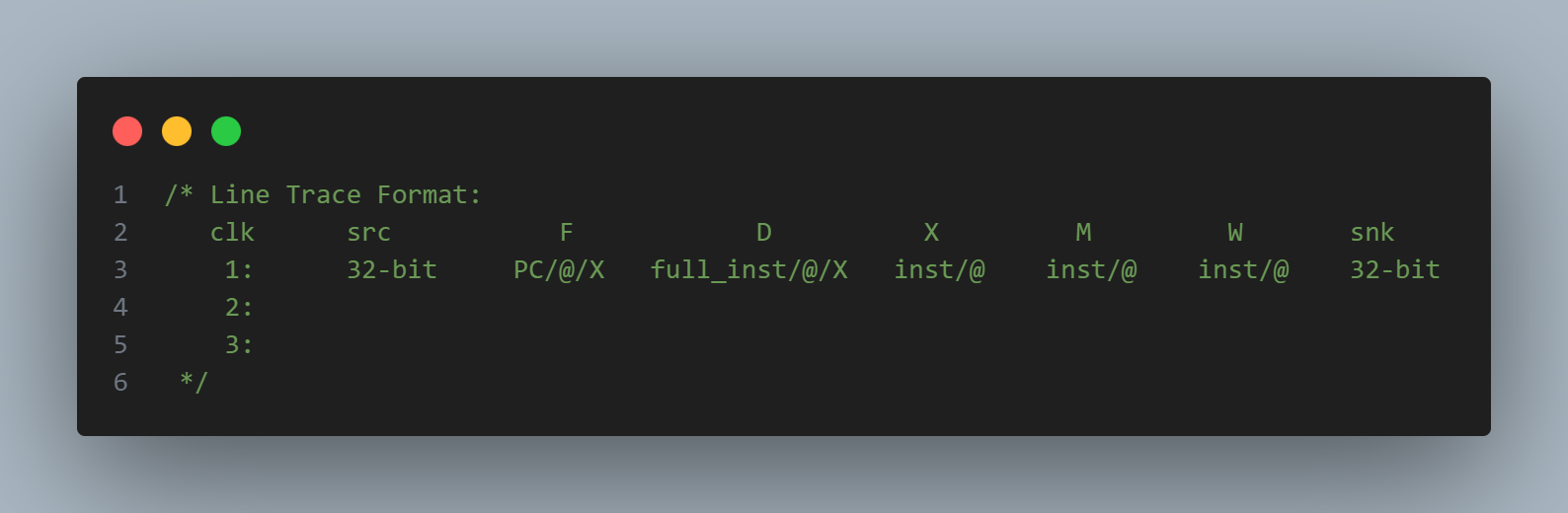
Figure 9. Format of Line Trace
"clk" means the clock cycle number. "src" represents the source message; when the register file is initialized, this column will display the values used to initialize the register file, otherwise, it displays nothing. "F" represents the F stage, where this column prints the PC value at the F stage. "D", "X", "M", "W" show the instruction executed at the current stage. For the F/D/X/M/W stages, if invalid, nothing is displayed; if stalled, an "@" is shown; if squashed, an "X" is displayed. The last column, "snk", represents the sink message; at the end of the program, we read the values from the register file using the csrw instruction and print them in this column.
We used three functions to implement the line trace functionality, as shown in the figure 10 below. The main functionality is implemented in the parseLog function, with decode and slice serving as helper functions.
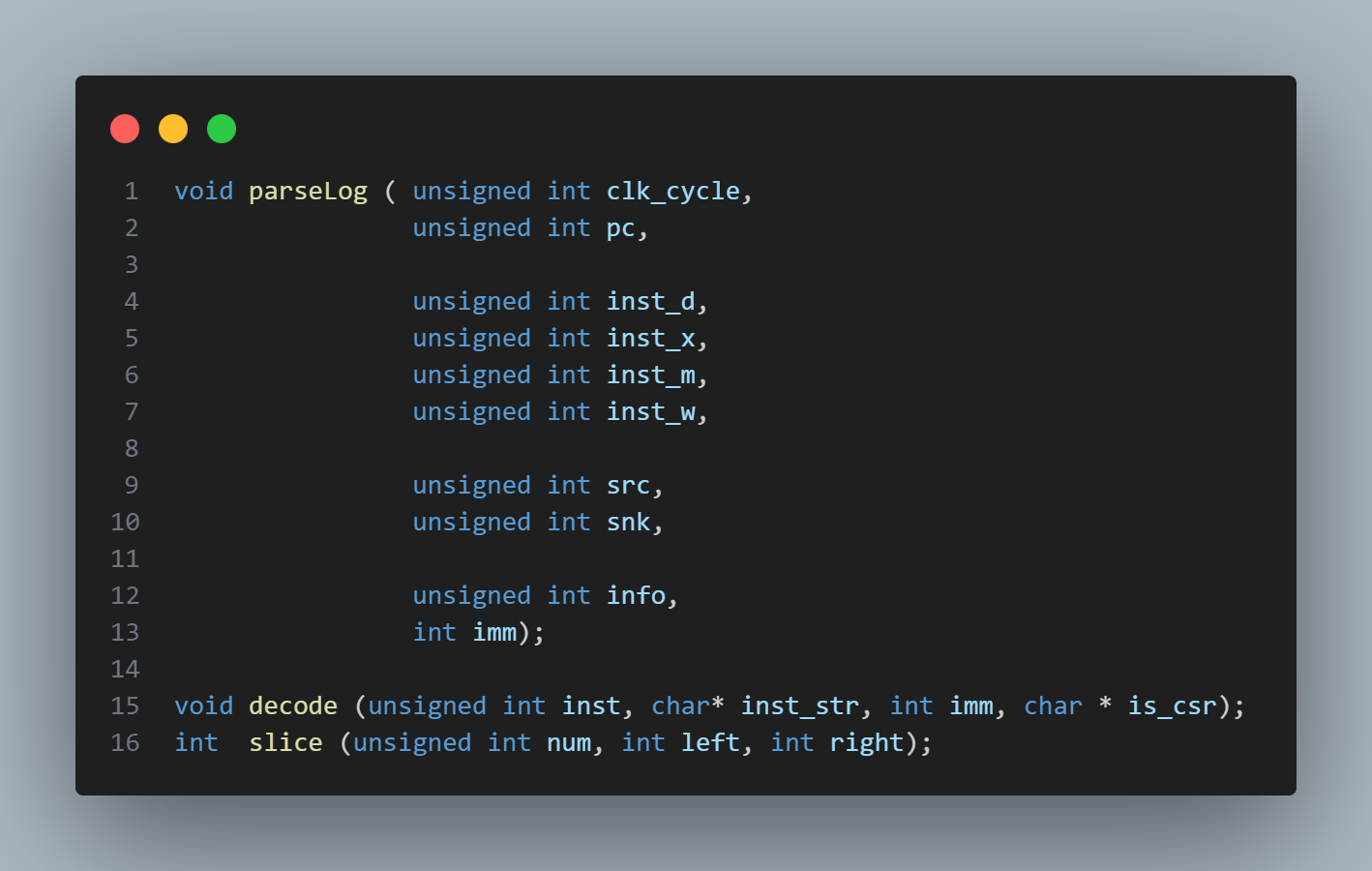
Figure 10. Functions to Achieve Line Trace
To achieve the line trace functionality, we need to obtain the following data from the FPGA and pass it to the parseLog function :
- clk_cycle: indicates the clock cycle number
- pc: indicates the PC value in the F stage
- inst_d, inst_x, inst_m, inst_w: indicate the instructions in the D/X/M/W stages respectively
- src: indicates the value from the source memory to the processor
- snk: indicates the value from the processor to the sink memory
- imm: indicates the immediate value obtained by the immediate generator in the D stage
- info: obtained by concatenation, with the lower 12 bits being valid. From high to low, the bits represent: val_f, squash_f, stall_f, val_d, squash_d, stall_d, val_x, stall_x, val_m, stall_m, val_w, and stall_w
Overall, the parseLog function prints a line trace to the terminal, which includes information such as clk, src, and F as previously mentioned. This function stores the information in strings like clk_msg, src_msg, and f_msg. Finally, it prints these pieces of information in a specific format. The specific implementation logic of parseLog is shown in the flowchart below (Figure 11).
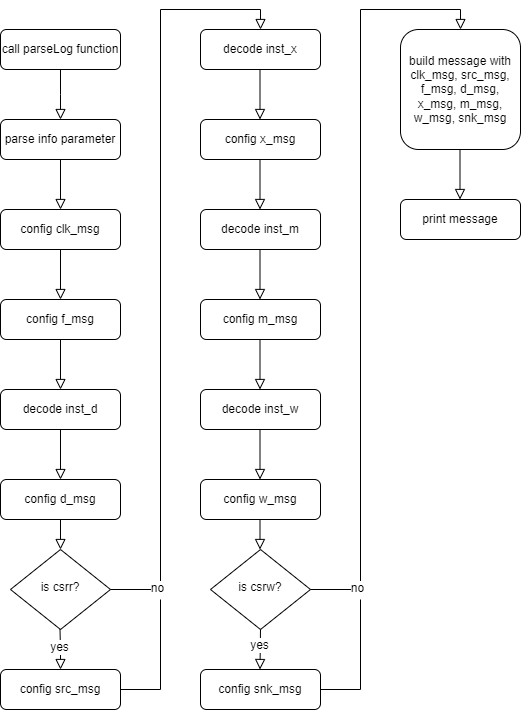
Figure 11. Flowchart of parseLog Function
First, the function parses the info parameter and stores it into 16 local variables (val_f, squash_f, ...). Then, based on these local variables, it configures the corresponding strings for each type of information, such as whether to print @ (stall), X (squash), or an instruction.
After parsing the info parameter, the function configures clk_msg and f_msg. Then, it calls the decode function (the specific implementation will be explained in the next section) to convert the 32-bit instruction back to the corresponding assembly code. After decode finishes, the function configures d_msg, x_msg, m_msg, and w_msg based on the return values of decode. Additionally, after decoding inst_d and inst_w, it needs to determine if they are csrr/csrw instructions to configure src_msg and snk_msg. Once all the substrings are configured, the function prints the line trace to the terminal in a specific format.
The implementation of the decode function is relatively simple. It has four parameters: inst and imm are data passed from the FPGA, inst_str is the assembly code corresponding to the 32-bit instruction, and is_csr is a flag indicating whether the instruction is csrr/csrw. The function determines the specific instruction based on the opcode, funct, and other information in inst, and converts it to the corresponding assembly code. The definitions of opcode, funct, and other information in inst are shown in Figure 12.
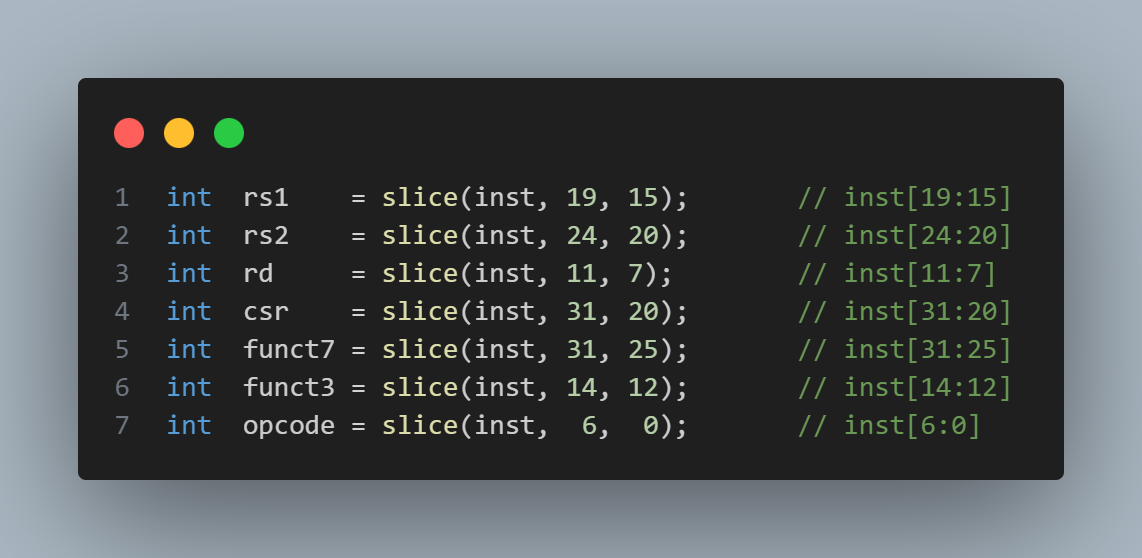
Figure 12. Instruction Format
4. VGA
For clarity, we plan to visualize several sorting algorithms, so we defined the VGA_update function. This function takes a pointer to the data memory as a parameter, assuming it contains ten data values. The function displays these ten values on the left side of the VGA screen. Each value is assigned a color, with larger numbers represented by brighter colors. This function also displays the color corresponding to each number on the right side of the VGA screen. During the visualization of the algorithm, we provide clock and reset signals to the FPGA from the ARM, and the VGA_update function is called at each clock cycle to update the VGA display.
ASSEMBLY
Our processor supports a subset of the RISC-V instruction set. We used the assembler provided in ECE 5740 (Python code) to convert the assembly code into three files. One is the machine code (.hex file). The other two are for source (.hex.in file) and sink memory (.hex.out file). Figure 13 shows an example of this conversion. The format of the machine code is “address: instruction”. The format of the source and sink files are just values. After that, the ARM reads these files and initializes the memory.
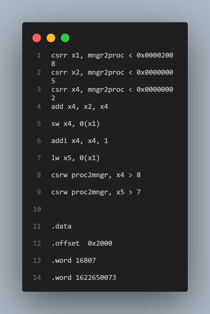
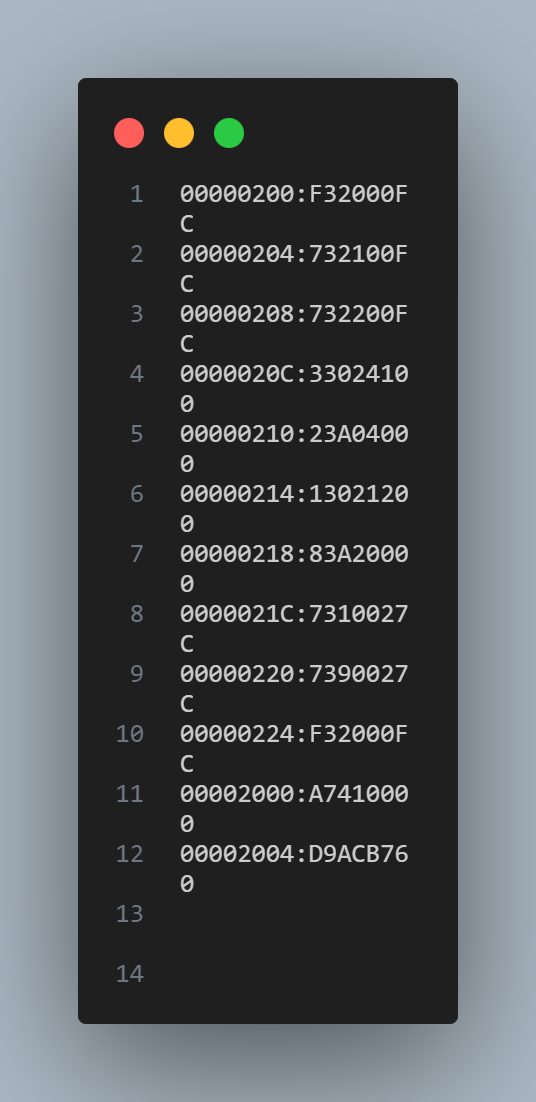
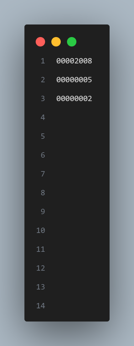
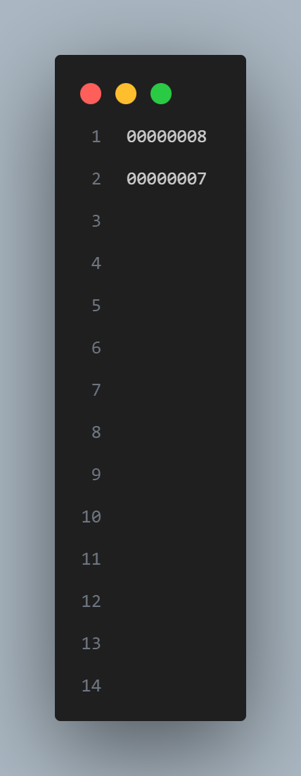
Figure 13. Example of Assembly Code Conversion, Left to Right: Assembly, .hex, .in, .out
We designed some assembly code to test our processor. We first verified the correctness of the csrr and csrw instructions. A value is written to a register using the csrr instruction, and then the value of the register is read using the csrw instruction to compare if the values are identical.
Then, for different types of instructions (a, b, c), we designed different assembly code to ensure the correctness of each individual instruction. For example, for the register-register instruction add, we used csrr to assign values to two registers, then executed the add instruction, and finally used csrw to compare the result. For the conditional branch instruction beq, we used csrr to assign the same value to two registers, then executed the beq instruction. If beq is executed correctly, the two instructions that change the register values following beq will be squashed. Finally, we used the csrw instruction to check if the register values matched the expected result.
After ensuring the correctness of individual instructions, we considered scenarios where multiple instructions interact, causing stalls and squashes. For example, the following example (Figure 14) includes all types of instructions, as well as situations causing stalls and squashes. The instructions on lines 5 and 6 (lw, add) cause a stall because the value of x2 is returned by mem in the M stage. When executing line 8 (beq) for the first time, no hazard occurs because the branch condition is not met. When this instruction is executed for the second time, the branch condition is met, and the two instructions following beq are squashed. The jal instruction also causes a squash, but it only squashes the instruction immediately following it. The specific waveform will be shown in the results section.
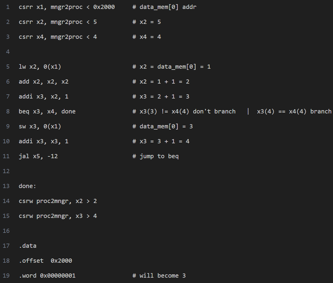
Figure 14. A Comprehensive Assembly Code
We also designed some commonly used code in real-world scenarios, such as bubble sort, selection sort, and insertion sort.
Results of the design
Modelsim result
Before running the code on the FPGA, we first conducted a simulation in ModelSim. This part was mainly divided into two sections: submodule test and system test. In the submodule test, we tested the mem, source, and sink modules. In the system test, we tested different types of instructions (types a, b, and c). After ensuring that individual instructions were correct, we tested scenarios that would generate stalls and squashes.
1. Submodule Test
This section tested the mem, source, and sink modules. The main focus was to verify whether the handshake signals (rdy/val) of these modules met the expected behavior.
In the mem testing, we modified memreq0_val, memreq0_msg, and memresp0_rdy, and observed whether memreq0_rdy, memresp0_val, and memresp0_msg matched the expectations. We tested both read and write operations of mem, and also examined the behavior when there was no handshake. As shown in Figure 15, mem functions correctly in both handshake and non-handshake scenarios. The green signals represent the input signals, and the blue signals represent the output signals.
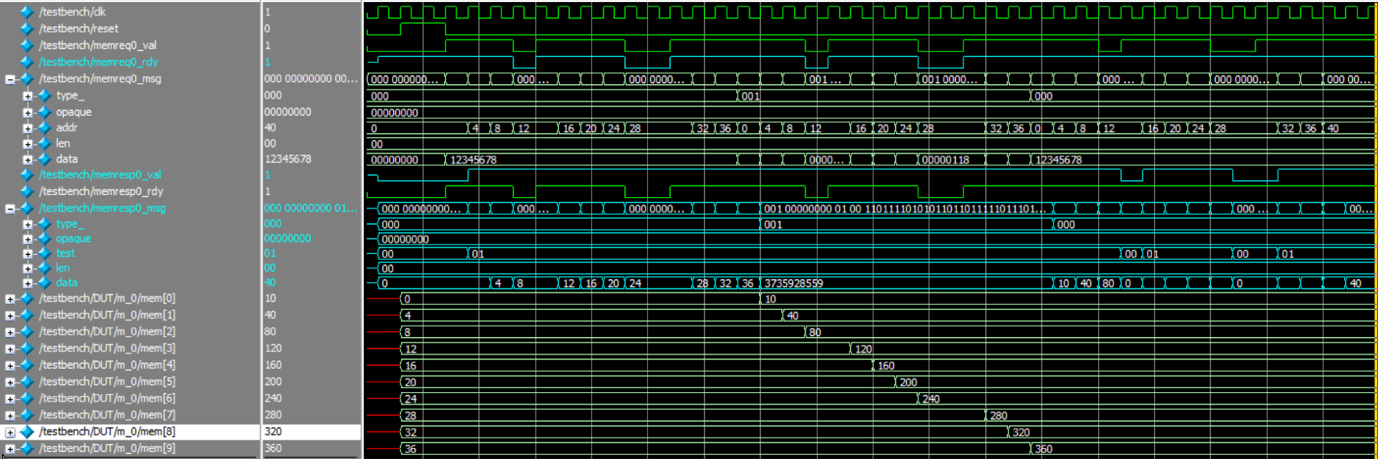
Figure 15. Mem Simulation
In the source testing, we assumed that the source memory contains 10 values. These values are used to initialize the register file. As shown in Figure 16, these values can be read out in the correct order (0x11111111, 0x22222222, ..., 0xaaaaaaaa). After the last value is read out, the done signal is asserted high, which matches our expectations.
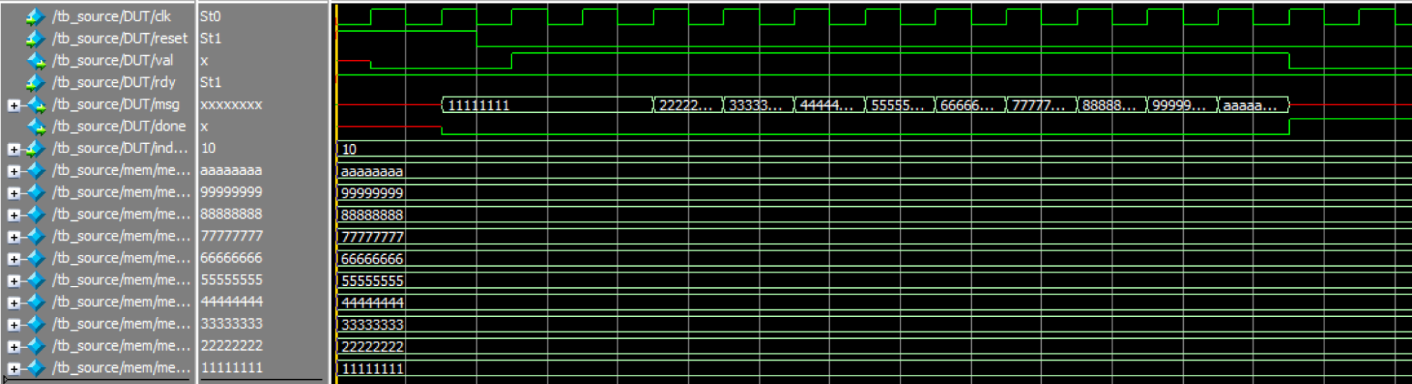
Figure 16. Source Simulation
In the sink testing, we also assumed that the sink memory would be written with 10 values. We wrote the values in sequence: 0x11111111, 0x22222222, ..., 0xaaaaaaaa. As shown in Figure 17, these values were correctly stored in the sink memory. After the last value was written to the sink memory, the done signal was asserted high, which also matches our expectations.
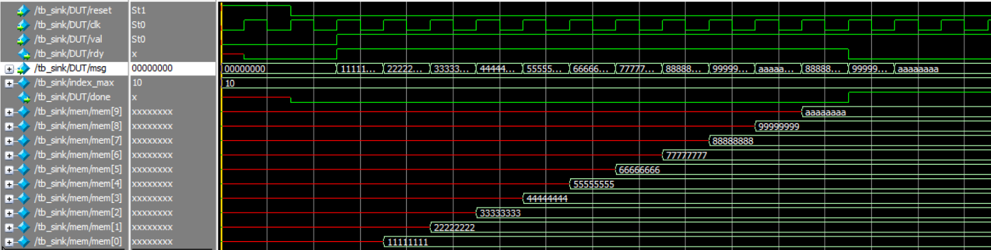
Figure 17. Sink Simulation
2. System Test
After ensuring the correctness of each submodule, we conducted a system test. In this part, we assembled the processor, initialized the instruction memory, data memory and source memory, and simulated some actual assembly code to observe if the behavior met our expectations.
This part of the testing took us a considerable amount of time. We first ensured
the
correctness of individual instructions, then considered scenarios where multiple instructions
interacted,
causing stalls and squashes. For clarity, we designed the following assembly code (Figure 18). This
assembly
code includes all types of instructions and considers situations that can cause stalls and
squashes.
Figure 18. A Comprehensive Assembly Code
From the waveform below (Figure 19.), it can be seen that when the program executes the add instruction (line 6), a one-cycle stall occurs because the value of lw needs to return at the M stage. Next, when the program first reaches the beq instruction (line 8), since x3 is not equal to x4, there is no branch and thus no squash. Afterward, the program executes the jal instruction, which is decoded in the D stage, causing a squash_F and jumping back to beq (line 8). When the program executes beq for the second time, the result of x3 equaling x4 is generated at the X stage, so the program branches to the done position, causing squash_D and squash_F.
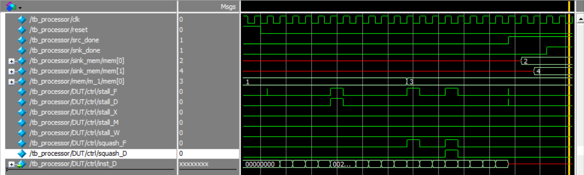
Figure 19. Waveform of The Comprehensive Assembly Code
Additionally, we tested more complex and realistic code, such as bubble sort, insertion sort, and selection sort. The figure 20 below shows the waveform for bubble sort. Initially, the 10 values are in random order, and when the program stops, the 10 values are sorted. This further demonstrates the accuracy of our processor.
Figure 20. Bubble Sort Simulation
On-board result
1. M10K read/write behavior test
The shared M10K memory in our design is used for the processor's memory, so the write and read timing issues are very important for further processor system construction. On-board tests are significant for us to check actual read and write behavior. The specific test method is that we first write some data into the M10K memory on the ARM processor, and the state machine on the FPGA side reads them out one by one and adds 1 to the read out values and writes them back. Then on the ARM side, it prints out the content of the memory and checks the correctness.
For the write operation, it takes one cycle to complete. For read operation, we initially believed that the read operation of the shared M10K dual-port on-chip SRAM would be delayed by one cycle, meaning the address input in the current cycle would produce an output in the next cycle. Based on this assumption, we wrote an initial version of the memory. However, after some simple testing, we found that the value of read_data changes at the moment the address changes. It seems a little weird for us that “combinational read” behavior could happen. Consequently, we rewrote the memory logic, which, fortunately, was simpler to implement under this condition and did not take much effort.
Later, we realized that this behavior could be configured in Qsys, allowing for either read logic to be implemented. This oversight cost us some time, highlighting the importance of thoroughly understanding the module configurations before usage.
2. Sink check
To check the functionality of instructions and arithmetic results on the reg files, we bring in the sink memory for it. In the assembly program, we utilize the instruction “csrw” to check the result of the reg files. When we read in the hex file of the assembly program, it takes out the expected value we put in the “csrw” instruction and stores it in an array. The final actual value of these registers will be written into the sink memory and we can read it out to check if they match expected value to verify that the instructions execute successfully.
The figure 21 below shows an example of how we utilize the sink memory to check the result.
In the first assembly program, we used the “csrr” instruction to load the value “5” into register x1, and check the content of it by the “csrw” instruction.
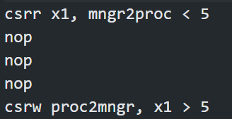
Figure 21. csrr & csrw example
We dumped the sink and source memory out after the processor had completed the instructions. Figure 22 shows the dumped memory. We can find the assigned value for register is successfully loaded into the source memory and the processor sends the value of register x1 into the sink memory.
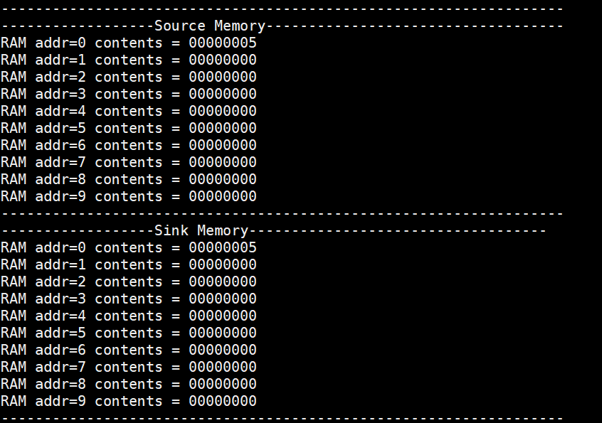
Figure 22. Final content of source and sink memory
By comparing the expected value and actual value of register x1, we can check if the processor runs the assembly program correctly. (figure 23)

Figure 23. Check content of registers
3. Memory check
Besides, we also dumped out the instruction memory, data memory to check the correctness of initializing the memory and the functionality of some memory related instructions.
For example, figure 24 shows an example assembly with “lw” and “sw” instructions.
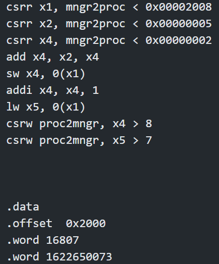
Figure 24. Memory check example
In the assembly program, we initialize the registers x1,x2 and x4 and then the processor will execute the “add” instruction between register x2 and x4, where the result will be stored in x4.
Then it will store the value of register x4 into the memory address that is stored in the register x1. After a “addi” instruction on register x4, it loaded the value back into the register x5 from the memory address that stored in register x1. Finally, we use the “csrw” instruction to check the content of registers. Besides, on the bottom of the assembly we initialize the first two locations of data memory with values “16807” and “1622650073”.
The figure 25 shows that the machine code converted from assembly instructions is successfully loaded into the instruction memory, and the initialization of data memory is also completed.
The addition result between register x2 and x4 which is “7” is also successfully written into the specified location ((0x2008-0x2000)>>2 = 3).
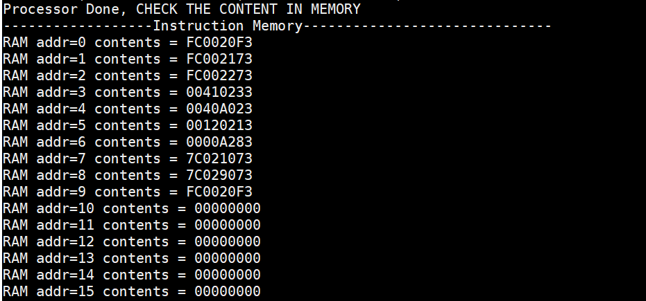
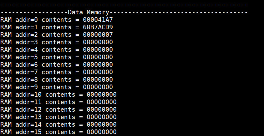
Figure 25. Check the content of memory
In figure 26, the source memory also had the expected initialization value of registers. The expected value of register x4 and x5 is 8 and 7, we read out the content of sink memory to check and both of them pass with expected final result.
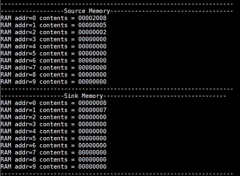
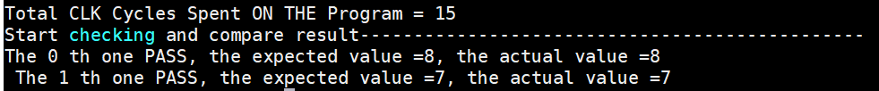
Figure 26. Check registers value with sink and source
The check process is quite convenient and useful to verify the functionality and demonstrate the final result of the assembly program. Here take an insertion sort algorithm as example, the initial data loaded in the data memory in the first 10 addresses are shown in the figure 27.
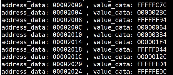
Figure 27. Initial content in data memory
The figure 28 shows that after running the insertion sort algorithm program, the data in the memory is rearranged from small to large.
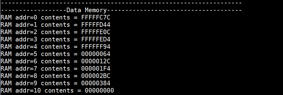
Figure 28. The content in data memory after running the sort algorithm program
4. Line trace
Figure 29 shows the line trace of a comprehensive assembly code mentioned in previou System Test section. This code includes each type of instruction and considers situations with stalls and squashes. As seen, in the 6th clock cycle, a stall occurs because the lw instruction requires the value of x2 to be returned from memory in the M stage, causing a one-clock cycle stall (indicated by @ in the line trace). In the 9th clock cycle, the program continues execution without squashing since the branch condition of beq is not met. In the 12th clock cycle, jal causes a squash (indicated by X in the line trace) in the F stage and jumps back to the beq instruction. In the 15th clock cycle, the branch condition is met, so the two subsequent instructions are squashed (in the F stage and D stage). The line trace shows that the processor's operation matches our assumptions and aligns with the simulation waveform mentioned in System Test.
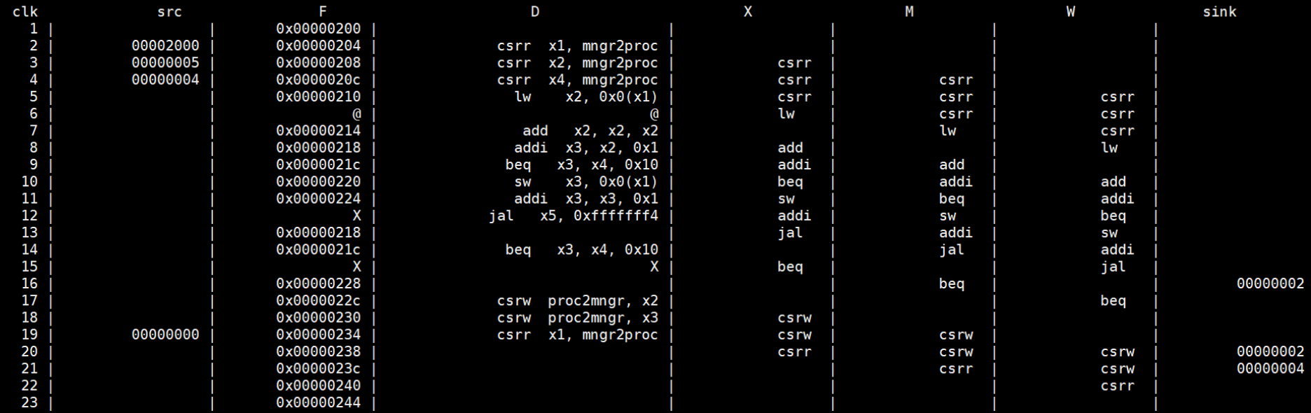
Figure 29. Line Trace of The Comprehensive Assembly Code
5. VGA color sorting
To better demonstrate the operation of the processor, we chose to visualize some sorting algorithms, including bubble sort, selection sort, and insertion sort. We fixed the first ten addresses in the data memory to store the data to be sorted and displayed this sorting process using VGA.
Specifically, we divided the right half of the screen into ten sections, each corresponding to an address from 0 to 9 in the data memory from top to bottom. The data at each address is represented by a color: the larger the number, the brighter the color; the smaller the number, the darker the color. The actual data values are displayed on the left half of the screen at the same height. As shown in figure 30, at the start, the data in memory is unsorted and the colors are randomly arranged. During the sorting algorithm execution, the colors gradually arrange from dark to bright from top to bottom.
Figure 30. VGA display before sorting
- Bubble sort: Compares two elements from top to bottom, placing the larger one below, and repeats this until the sorting is complete.
- Selection sort: Finds the smallest element in each iteration and places it in the first position, then finds the second smallest and places it in the second position, and so on.
- Insertion sort: Builds a sorted sequence by scanning from the end of the already sorted sequence and inserting each element in its correct position. It starts by considering the first number in memory as a sorted sequence and then inserts each subsequent number in order.
The final result is shown in figure 31, with the numbers arranged from smallest to largest from top to bottom, and the colors from darkest to brightest.
Figure 31. VGA display after sorting
Resource utilization
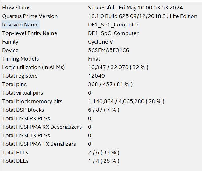
Figure 32. Resource utilization
It can be seen from the figure above that the most utilized resource on the board is the pins. This is likely due to the complex internal connections of the processor. In contrast, computational logic resources are not heavily utilized, as there is not much computational logic involved. The Chip planner below shows more details of the resource utilization.
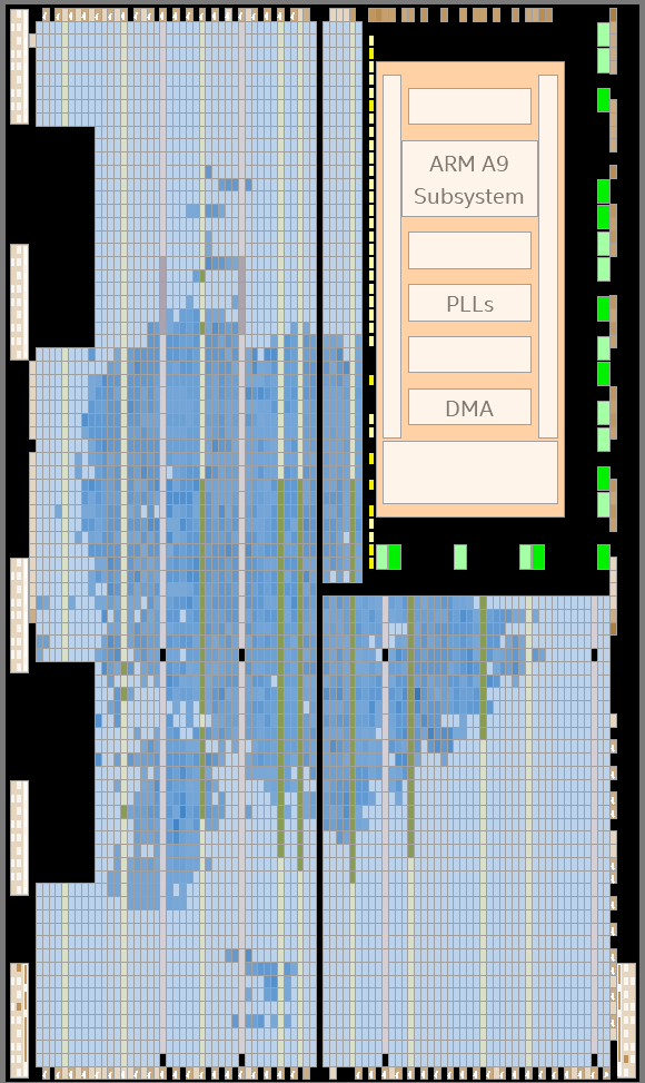
Figure 33. Chip planner
Speed of execution
To display the line trace during execution and visualize the sorting algorithms, we chose to use the HPS to provide the clock signal to the processor. This ensures the processor runs at a slower speed. However, during the design process, we initially used the 50MHz clock internal to the FPGA, which allowed the processor to operate correctly. Therefore, we know that the fastest frequency at which our processor can execute operations is 50MHz.
Safety
In our project, we used only one DE1-SoC board, so there are no additional safety hazards. We only need to follow proper power operation procedures and return the board to the cabinet promptly after use to ensure safety.
Usability
Although our project is closely related to the ECE 5740 Computer Architecture course, even those unfamiliar with the course can still operate the processor we designed. By loading the project onto the FPGA and running our C program, they can run their own assembly programs on the processor (though some basic knowledge of assembly language and RISC-V ISA is likely still required). However, for those who have taken the course or have studied related material, our project will be very easy to understand and use.
Conclusions
Our design perfectly met our expectations. We successfully implemented a five-stage pipelined processor supporting the RISC-V subset TinyRV2 on an FPGA. It can be operated by running a C program on the HPS, which reads hexadecimal machine language data generated from an assembly program, initializes memory and source, and then controls the processor's operation by sending clock signals. During operation, the line trace is drawn cycle by cycle based on internal information to monitor the processor's performance at each stage. After execution, the memory content is extracted and printed to verify if it matches expectations, and the data received by the sink is compared to the specified assembly program data, all of which help to check the correct operation of the processor. Additionally, to make the processor's operation more intuitive and understandable, we visualized the bubble sort, selection sort, and insertion sort algorithms on a VGA display, using color brightness and block arrangement to represent the sorting process.
Our design fully supports the TinyRV2 subset of RISC-V, correctly executing each specific instruction and properly handling data and control hazards, making it capable of running C programs that do not use system calls.
Our project is highly expandable and can accommodate various architectural enhancements. For example, we could add a cache between the processor and memory, introduce a branch predictor to optimize performance when processing branch instructions, or expand the processor into a multi-core system. Additionally, we could implement system designs such as designing a simple operating system to run on the architecture.
The inspiration for our processor design and some of the code came from Lab 2 of the Cornell ECE 5740 Computer Architecture course. After consulting with the course professor, we confirmed that the code could not be publicly shared and will only be privately sent to lecturer Van Hunter Adams. However, all materials outside of the course-related code can be found on the course website for those interested.
Altera's IP used in this project includes the VGA subsystem driver, shared M10K dual-port on-chip SRAM, and PIO.
Regarding patent opportunities, parts of our code come from the ECE 5740 course and do not belong to us, and the ISA supported by this processor is the open-source RISC-V, so there are no patent opportunities.
Appendix A (permissions)
- "The group approves this report for inclusion on the course website."
- "The group approves the video for inclusion on the course youtube channel."
Appendix B
Codes:
Since our project utilizes some of the code from the labs in the ECE 5740 Computer Architecture course, it cannot be publicly displayed due to potential use in future course materials. Codes will only be privately sent to lecturer Van Hunter Adams.
Task distribution
All members participated in debugging, integration, and documentation. Shuzhe Liu, Tongyuan Liu and Jiacheng Tu worked together for the entirety of the project.
References:
DE1_SoC: https://vanhunteradams.com/DE1/Lorenz/Getting_Started.html
VGA video at 640x480 displayed from SDRAM, in 16-bit color: https://people.ece.cornell.edu/land/courses/ece5760/DE1_SOC/HPS_peripherials/Examples_version_18.html
ECE 4750: Computer Architecture, https://www.csl.cornell.edu/courses/ece4750/
ECE 4750 Lab 2: Pipelined Processor, https://www.csl.cornell.edu/courses/ece4750/handouts/ece4750-lab2-proc.pdf
Tiny RISC-V Instruction Set Architecture, https://www.csl.cornell.edu/courses/ece4750/handouts/ece4750-tinyrv-isa.pdf