Superscalar Out-of-Order NPU Design on FPGA
2024 Spring ECE5760 Final Project by Yuqiang Ge (yg585), Kapinesh Govindaraju(kg534), Sona Susan Jacob(sj778)
Project Video
1. Project Introduction
In this project, we built a NPU (Neural Processing Unit) with VLIW superscalar out-of-order processing architecture on DE1-SoC for acceleration of matrix computations.
An NPU is a specialized hardware accelerator designed specifically for accelerating the computations involved in neural networks. Unlike general-purpose CPUs or even GPUs, which can handle a broad range of tasks, NPUs are optimized for the specific computational patterns and data flows of neural network workloads.
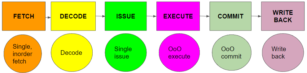
The NPU (basically a processor) we designed has special functional units like matrix addition, matrix dot, matrix convolution, ReLU, etc. The motive of the functional units in the processor is to ultimately run a full CNN model at higher computational speeds. With the help of 128 bit sized instruction set our project aims to differentiate between the various operations of the functional units with unique opcode values. Our processor is a superscalar, Out of Order in nature with six stages: Fetch, Decode, Issue, Execute, Commit, and Write Back.
The processor follows the single fetch and single issue architecrture, while it's out-of-order execution and out-of-order commit. The write-back stage results and updates the status flags. The functional units work in parallel for the processor. 12 SRAMs are utilized incorporating the functionality of banked memory subsystems. The functional units will make use of these SRAMs as Data memory. There is also an extra SRAM module for instrunction RAM. Our entire processor design is scalable in nature since we can keep adding more functional unit modules to enhance its usage.
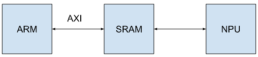
In the system, the ARM CPU primarily handles the control of the NPU to carry out computations. It is also responsible for reading the input image data and weights trained by PyTorch and writing the data into SRAM for use by NPU.
2. High Level Design
2.1 High Level System Architecture
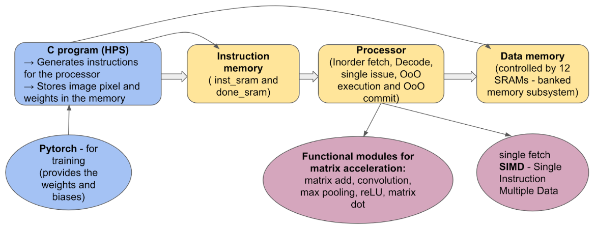
The high-level design of the Neural Processing Unit is a superscalar out-of-order processor architecture with various functional units designed to execute CNN operations. The structure of the NPU is made up of the Instruction Set Architecture, Functional Units, Memory Subsystem, Processor Pipeline, and Clock Domains.
The ISA is following a 128-bit wide instruction format. The ISA also provides details on encoding the source and the destination addresses and parameters like the matrix dimensions. Each instruction's computation is handled by a dedicated functional unit. The function units consist of convolutional units (Conv1, Conv2, Conv3) for different channels, matrix addition, subtraction, element-wise multiplication, matrix multiplication, ReLU, and max pooling. Each unit is independent and can process various instructions simultaneously.
High-Level View of System Architecture
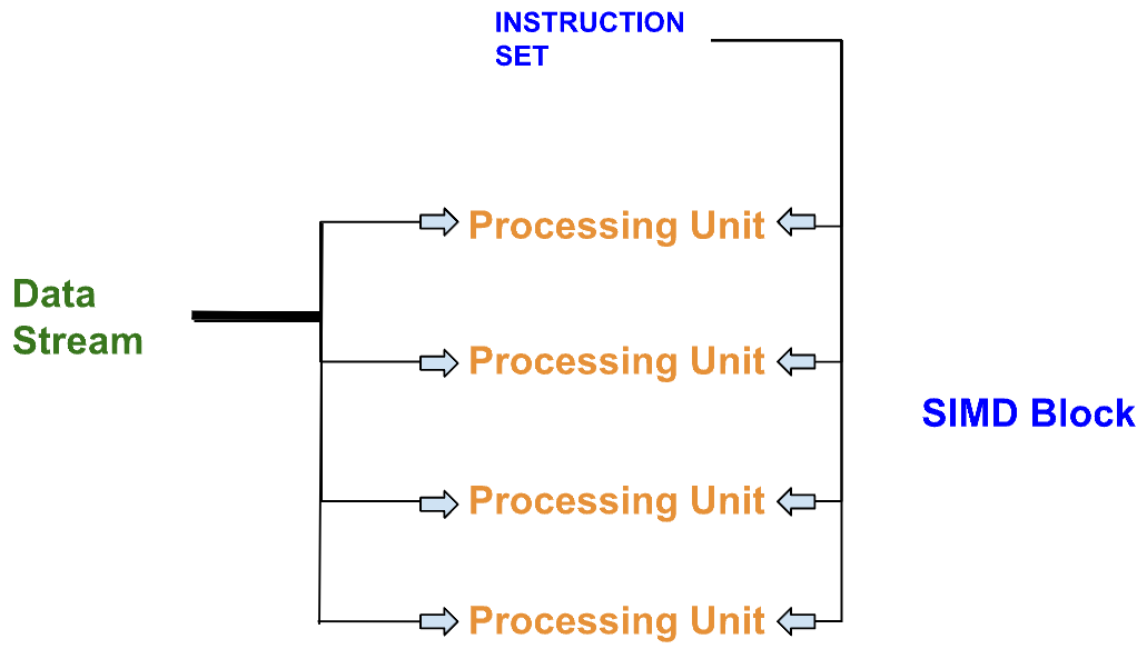
Given that matrices involve a large amount of data, our computational architecture is designed as SIMD (Single Instruction, Multiple Data). This approach allows for the simultaneous processing of multiple data points with a single instruction, making it highly efficient for operations involving large matrices.
SIMD Block Diagram
The instructions are sent to a onchip SRAM, which is configurd to be instruction RAM . Fetch stage of the processor basically gets the instructions from the onchip SRAM. Decode stage of the processor assigns the memory address locations for the sources and destination. We use 12 SRAMs for the data memory, each having data width as 16 bits and memory size as 32,768 bytes. Each of the SRAMs will have the capability to store a 128 x 128 pixel image within it, and each pixel is 16 bits. The SRAMs will work like a Banked Memory Subsystem along with out of order processing.
There are totally 9 functional units in our design and each of the functional units will have access to all SRAMs as specified in the instrunction. This is made possible by having a complex routing network. Multiplexers are used for this purpose (to connect signals from the SRAM to the functional units and vice versa). Issue stage will assign the starting addresses for the source and destination. It will also provide the start signal for the corresponding functional module considered. The start addresses are passed on from the Decode stage.
We are using Out of Order Commit since we are assuming that there are no dependencies between the instructions. Incase of handling dependencies to control logic might become complex. Constructing a reorder buffer might solve that condition. A commit buffer is used incase two instructions want to commit at the same time. Our processor has the ability to handle multiple commits at the same time due to the presence of this commit buffer. But in the Write Back stage we use Round Robin Arbitration scheme to write the done signal into the SRAM so that the ARM can know that instructions are fully done. We have a done SRAM and provide it with 1s in an Out of Order fashion based on the function completion.
We use standard interfaces (includes all the required signals like source address, destination address, row and column parameters, etc.) for all our functional units so that it will become easily compatible with the processor design and it allows for us to always hookup any new functional units to the processor based on the requirements.
The SRAM is running at 250 MHz and so due to that in our functional units we can treat the SRAM as a combinational one. Also it is to be noted that since our functional units are entirely independent of each other, They are capable of reading, performing necessary calculations and writing back to the onchip SRAM simultaneously.
We have trained everything on PyTorch and we used the MNIST dataset for training. After training, the accuracy of 5 epoch is found to be 96% accurate. We can take the image from the PyTorch and allow it do all the normalization and preprocessing required on the image.
For inference on the NPU, we have implemented a C program, including a compiler and driver that can compile the required operations into instructions and send them to the NPU for inference. This program can read in weights trained by PyTorch, write the weights to the NPU, and then the NPU performs the computations. Finally, the C program can read the computational results from the NPU. It should be noted that during the execution of instructions, no other instructions should use the same block of SRAM until the previous instructions are completed.
2.2 Rationale and Sources of Project Idea
We got the idea for this project by looking at the advancements made by tech giants, who have developed their own AI-specific hardware. Inspired by their success and academic research, we saw the potential for creating a similar accelerator tailored for educational purposes. The DE1-SoC platform was chosen because it offers a great environment for developing and testing our NPU. An NPU can be used in various applications, from enhancing AI performance in smartphones and IoT devices to serving as a learning tool for students and researchers. By combining industry trends, academic insights, and cutting-edge technology, our goal is to build a powerful, energy-efficient NPU that meets the needs of AI applications.
2.3 Background Knowledge
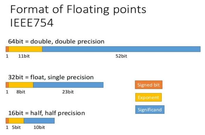
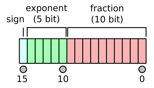
2.3.1 Floating Point: We used floating point floating point 16, we chose this over floating point 32. We used a floating point over a fixed point since it gives high accuracy. The 16-bit floating point is known as half-precision. The floating point 16 has a Sign Bit (1 bit) that determines the sign of the number (0 for positive, 1 for negative). Exponent (5 bits), used to store the exponent of the number. Mantissa (10 bits), also known as the significand or fraction, stores the significant digits of the number. FP16 is a binary floating point format that takes 16 bits in the computer memory. The exponent is stored with a bias of 15, the actual value of the exponent is obtained by subtracting 15 from the stored exponent value. The exponent ranges from -14 to +15. The special cases are represented as follows: Zero, which is represented by all bits set to zero. Infinity is represented by an exponent of 31 (all bits set to 1) and a mantissa of 0. NaN (Not a Number) is represented by an exponent of 31 and a non-zero mantissa. The precision is determined by the number of bits in the mantissa. In our case, FP16 has approximately 3 decimal digits of precision.
Floating Point Formats
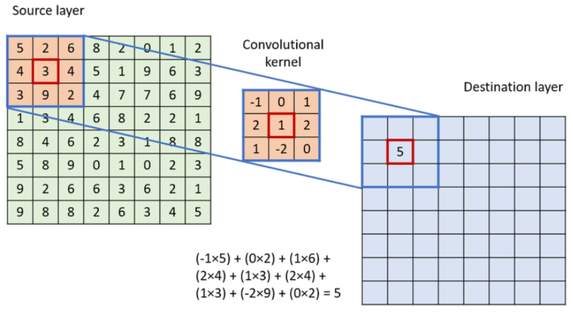
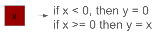
2.3.2 Convolution: The Convolution operation involves the mathematical process where a kernel is applied to an input matrix to produce an output matrix. This operation helps in detecting the local patterns. The input matrix represents the image or data that is processed. We considered a square matrix for our convolution operation. The kernel is a smaller matrix that slides over the input matrix. The kernel performs element-wise multiplication with overlapping regions of the input matrix and sums the results to a single value in the output matrix. The output matrix is the result of the convolution operation and the size of the output matrix depends on the input size and kernel size. The kernel is placed at the top left corner of the input matrix initially. The element-wise multiplication is performed and the result is then placed in the corresponding position in the output matrix. The kernel is moved across the input matrix and the number of pixels the kernel moves each time is called stride. The convolution operation is performed for each new position. Once the entire input matrix has been covered by the kernel, the process stops.
Convolution Operation
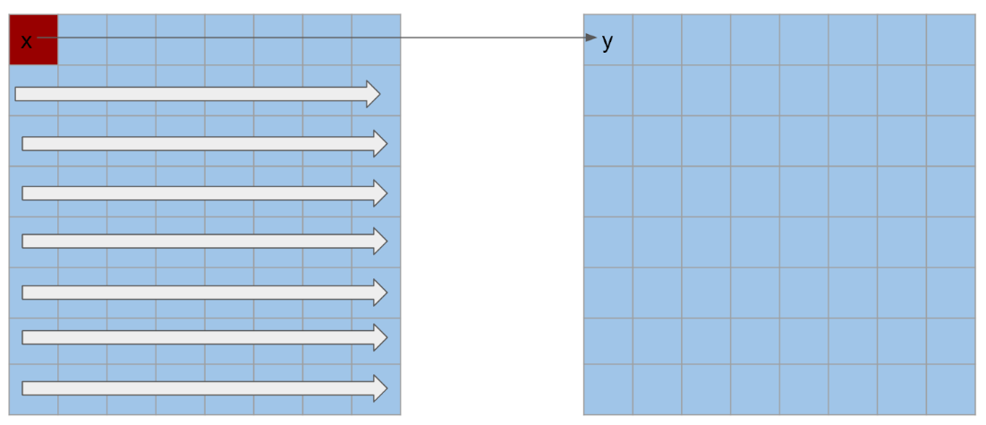
2.3.3 ReLU : The ReLU (Rectified Linear Unit) activation function is widely used in neural networks due to its simplicity and effectiveness in introducing non-linearity to the model. The primary purpose of ReLU is to allow neural networks to learn complex patterns by enabling them to approximate non-linear functions. Mathematically, ReLU is defined as f(x)=max(0,x), meaning that it outputs the input directly if it is positive; otherwise, it outputs zero. This non-linear transformation helps in addressing the vanishing gradient problem, where gradients used for updating weights in deep networks become very small, hindering the learning process. ReLU mitigates this by providing a constant gradient for positive inputs, thus facilitating efficient and faster training. Additionally, by setting negative values to zero, ReLU introduces sparsity in the network, which can improve computational efficiency and reduce the risk of overfitting by making the network less sensitive to small variations in the input data.
ReLU Operation
ReLU Operation
2.3.4 Max-pooling: Max-pooling is a down-sampling operation commonly used in convolutional neural networks (CNNs) to reduce the spatial dimensions of the input matrix while retaining the most significant features. The primary purpose of max-pooling is to reduce the computational complexity of the network, improve efficiency, and provide spatial variance. In max-pooling, a filter (or window) of a specific size slides over the input matrix, and for each position, it outputs the maximum value within that window. This operation effectively compresses the input by summarizing the most prominent features, which helps in mitigating the risk of overfitting. By focusing on the strongest responses, max-pooling also provides a form of translational invariance, ensuring that small shifts or translations in the input do not significantly affect the pooled output. This property is crucial for tasks like image recognition, where the exact position of features might vary slightly across different images.
Max-pooling Operation
2.3.5 Fully Connected: The fully connected layer plays a crucial role by integrating learned features from prior layers to form the final output. Each neuron in a fully connected layer is connected to all the neurons in the previous layer. This layer essentially takes an input volume and outputs an N-dimensional vector where N is the number of classes that the program is trying to classify. For instance, in a facial recognition scenario, this output vector could represent different individuals' faces that the model is trained to recognize. The fully connected layer maps the extracted features into the final output categories through learned weights, making it essential for pattern recognition tasks within CNNs.
Fully Connected Operation
2.3.6 Processor Architecture: The idea of the principle of working of the Superscalar processors can use multiple instructions per clock cycle and requires knowledge of instruction-level parallelism and how multiple units can be utilized. The out-of-order execution techniques allow the instructions to be executed as soon as their operands are available instead of following the program order.
2.4 Tradeoffs
CPU vs NPU: CPUs offer general-purpose computing versatility and can handle a broader range while NPUs provide specialized, high-speed computational tasks for specific functional units. In our system, NPU is responsible for matrix calculation, While CPU is responsible for control.
Performance vs. Precision: Using floating-point 16-bit precision offers a balance between computational speed and accuracy, though it sacrifices some precision compared to 32-bit floating point.
Complexity vs. Clock Speed: Running the processor core at 100 MHz and functional units at 25 MHz introduces complexity in clock domain synchronization but allows for higher overall throughput.
Memory Bandwidth vs. Complexity: The banked SRAM architecture allows for the high memory bandwidth necessary for parallel matrix operations but increases the complexity of memory management and routing.
3. Software Design
3.1 128-bit Instruction Set Design
The 128-bit instruction set architecture is designed to handle a variety of matrix operations supported by the NPU processor, with each instruction encoded in a structured format. The architecture includes instructions for addition (ADD), convolution (CONV, CONV2, CONV3), pooling (POOL), activation functions (RELU), subtraction (SUB), element-wise multiplication (MULT), and matrix multiplication (DOT).
For most instructions, the fields include opcode, source arrays address, destination array address, and size of the arrays. This consistent format ensures that the instructions are easy to decode and execute, facilitating efficient processing.
However, the DOT instruction is designed differently to accommodate the specific requirements of matrix multiplication. Unlike other instructions, the DOT instruction's lower 28 bits are encoded differently. This is because, in matrix dot product, the number of columns in the first matrix equals the number of rows in the second matrix, requiring only three parameters. This design choice allows the instruction set to use the limited bit space more efficiently, supporting larger matrix sizes.
The instruction set is shown in the table below:
| Bits | 124-127 | 92-123 | 60-91 | 28-59 | 19-27 | 10-18 | 8-12 | 0-7 |
|---|---|---|---|---|---|---|---|---|
| ADD | 0001 | &src1 | &src2 | &dest | src1_row | src1_col | reserved | reserved |
| CONV | 0111 | &src1 | &src2 | &dest | src1_row | src1_col | src2_row | src2_col |
| CONV2 | 1001 | &src1 | &src2 | &dest | src1_row | src1_col | src2_row | src2_col |
| CONV3 | 1011 | &src1 | &src2 | &dest | src1_row | src1_col | src2_row | src2_col |
| POOL | 1000 | &src1 | &src2 | &dest | src1_row | src1_col | src2_row | src2_col |
| RELU | 1010 | &src1 | &src2 | &dest | src1_row | src1_col | src2_row | src2_col |
| SUB | 0010 | &src1 | &src2 | &dest | src1_row | src1_col | reserved | reserved |
| MULT | 0011 | &src1 | &src2 | &dest | src1_row | src1_col | reserved | reserved |
| Bits | 124-127 | 92-123 | 60-91 | 28-59 | 16-27 | 8-15 | 0-7 |
|---|---|---|---|---|---|---|---|
| DOT | 0110 | &src1 | &src2 | &dest | src1_row | src1_col | src2_row |
3.2 Compiler Design
We implemented a simple C compiler function that generates a 128-bit instruction based on user input. The function accepts an opcode as well as source addresses 1 and 2, a destination address, and matrix row and column information as inputs, and returns a 128-bit instruction.
In the code, we defined a structure named 'uint128_t' that contains two 64-bit unsigned long integers, 'low' and 'high', representing the lower 64 bits and the upper 64 bits of the 128-bit instruction, respectively. The function 'gen_inst' initializes a 'uint128_t' variable named result to store the generated instruction.
During the instruction generation process, the function compares the input opcode op using the strcmp function and writes the corresponding binary encoding to the upper 4 bits of result.high. For instance, if the opcode is "ADD," 0x1ULL is shifted left by 60 bits and stored in result.high using a bitwise OR operation. Other opcodes, such as "CONV" and "POOL," are processed similarly. The information for source addresses 1 and 2 and the destination address is written into result.high and result.low using bitwise operations. Additionally, the matrix row and column information is written into different positions within result.low. It is important to note that there is special handling for the "DOT" opcode, as its instruction format differs slightly from other opcodes. Finally, it stores the instruction in the instruction pointer inst_ptr, which points to the instruction SRAM.
3.3 Driver Design
In this system, a C driver runs on the ARM CPU to control the operation of the NPU. This driver can access the SRAM mounted on the AXI bus via addressing. The NPU can read from or write to these SRAMs, facilitating communication between the ARM and the NPU.
In the C driver, we use 'mmap' to obtain a virtual address pointing to the physical SRAM, enabling access to the SRAM through Linux management. The address of SRAMs are configured in Qsys. It is necessary to use the same address here for memory access. The C driver can write instructions to the "Instruction SRAM", read from and write to the "Data SRAM", and read the "Instruction Done SRAM" to check whether instructions have been completed.
It's important to note that the data SRAM is 16-bit, while memory addressing is byte-oriented. Therefore, when accessing memory via pointers, incrementing the pointer variable by one means the memory address points to a position two bytes ahead.
3.4 CNN Training in PyTorch
3.4.1 Neural Network Architecture
We implemented a simple Convolutional Neural Network using Pytorch. The network has only one convolution layer. The architecture of this network is as follows:
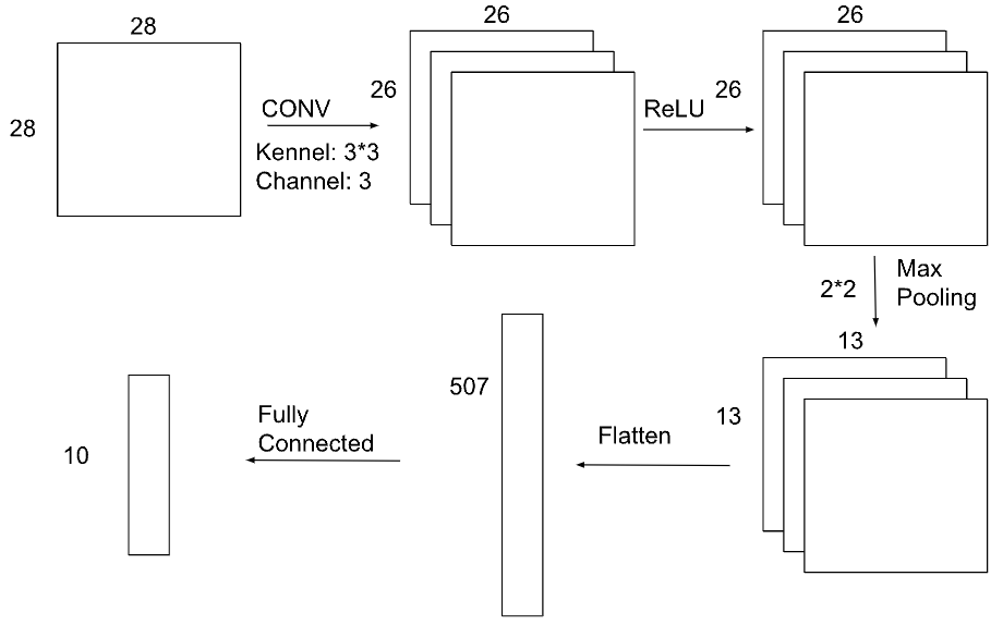
CNN Architecture
1. Convolution Layer: The input channel is 1, the output channel is 3, with a kernel size of 3x3.
2. ReLU Activation.
3. Pooling Layer: Maxpooling layer. The kernel size is 2*2. The stride is 2.
4. Flatten Layer: Used to flatten the multidimensional input into a one-dimensional vector.
5. Fully Connected Layer: The input size is 13x13x3, the output size is 10.
During the forward pass, the input first goes through the convolution layer, followed by the ReLU activation function, and then through a max-pooling layer. Next, the data is flattened and passed through the fully connected layer, and the final output is produced.
3.4.2 Neural Network Training
The dataset used is the MNIST handwritten digits dataset, with the following preprocessing steps:
1. Transform to Tensor (ToTensor): Converts image data to PyTorch tensors.
2. Normalize (Normalize): Normalizes the image data to have a mean of 0.5 and a standard deviation of 0.5.
After preprocessing, the dataset is loaded into training and testing data loaders, with a batch size of 64.
The model uses Cross-Entropy Loss and the Adam optimizer for training. The model is trained for 5 epochs, with each epoch iterating over the training dataset once.
After training, the model is evaluated on the test set to calculate accuracy and output the results. The accuracy of this model is 96 % after training for 5 epoches.

CNN accuracy
The trained weights are stored in csv files, which can be used for the inference using NPU.
3.5 Inference on NPU
To perform inference on the NPU, considering the complexity of normalization, we first normalize the MNIST image data in PyTorch and output it to a CSV file. The normalized data can be directly used by the NPU. Alternatively, a normalization function can be implemented in the C program, allowing the raw image data to be read directly into the C program and normalized before being passed to the NPU for inference.
For inference on the NPU, we first need to read the data from the CSV file. This data includes the trained weight parameters from PyTorch and the image data to be inferred. Once the data is read, it must be written into the NPU's SRAM. The AXI bus interface is used to handle data transfer between the ARM CPU and the SRAM efficiently.
After writing the data, we can call the compiler function to generate the corresponding instructions. Since we trained a single layer network in PyTorch, we need to control the NPU to perform the same computation during inference. The NPU contains three convolution modules, allowing us to run three convolution channels simultaneously. After the convolution operations, the results of the three channels undergo ReLU activation. Following the ReLU activation, pooling is performed, and then a fully connected layer is executed. Finally, the C program reads the matrix data output from the fully connected layer in the SRAM. The entry with the highest value is the inference result.
4. Hardware Design
4.1 Hardware Architecture
Hardware Architecture
In our system, the hardware primarily consists of three components: the ARM CPU, the NPU on the FPGA, and the SRAM for communication between the ARM and FPGA. The ARM CPU is mainly responsible for sending instructions and read/write the SRAM, while the NPU on the FPGA handles computations. The SRAM serves as storage for instructions and data, facilitating communication between the ARM CPU and the NPU.
4.2 Processor Architecture
Processor Pipeline
The processor is a superscalar out-of-order processor that supports a 128-bit very long instruction word. It includes nine functional units, each designed to processing a specific type of instruction. These units are capable of executing operations such as convolution, pooling, ReLU activation, and common matrix computations, supporting a wide array of computational tasks. The processor's architecture features a six-stage pipeline: fetch, decode, issue, execute, commit, and write-back. As shown in the figure above.
In the fetch stage, the processor retrieves instructions from memory using a single in-order fetch mechanism, checking each for validity. A valid instruction increments the instruction pointer. Then the instrunction is pipelined to the decode stage, where it is decoded according to the specifications of the instruction set architecture. This decoding process generates control signals that manage the operation of the functional units and the multiplexer network facilitating communication between the units and memory.
During the issue stage, control signals are sent to the respective functional units. Control signals include: start address of matrices, size of matrices, multiplexer selection signal(used by the routing network), and start signal. In the execute stage, functional units start computing upon receiving a 'start' signal. After computation, each unit sends a 'done' signal that is returned out-of-order. A commit buffer is employed to handle situations where multiple completion signals occur at the same cycle. The commit buffer can successfully capture the commit information. In the write-back stage, the commit information is write back to SRAM.
During the write-back stage, the execution results of the instructions are written into the “Instruction Done SRAM”. The processor continuously checks the commit buffer using a polling strategy. If it detects instructions that need to be written back, the processor writes the instruction completion information into the "Instruction Done SRAM". Meanwhile, the ARM CPU constantly polls the "Instruction Done SRAM". If an instruction is found to be completed, the ARM processor can then use the results in the SRAM for further operations.
It should be noted that this processor operates under a frequency of 100 Mhz. However, due to the use of floating-point calculations, all functional units operate at 25 Mhz, making it necessary for both the start and done signals to cross clock domains. For example, in the issue stage, the 'start' signal is sent from 100 Mhz to 50Mhz. In this processor, a handshake mechanism is utilized to manage the crossing of clock domains for the start and done signals. The start signal remains high until the done signal goes low, at which point the start signal can return to low.
The routing network that connects the functional units and SRAMs in the system is comprised of multiplexers. The signals for address, writedata, and write enable are all output from the functional units and received by the SRAM. As such, the same type of multiplexer is used for these signals. In this processor, we use a 25-to-1 multiplexer for these signals. However, read data flows from the SRAM to the functional units, requiring a different type of multiplexer. For this data flow, we use a 16-to-1 multiplexer in our processor.
4.3 Memory System
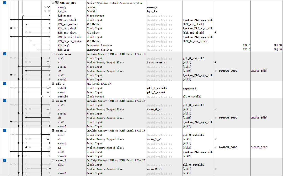
The memory design of this processor is quite unique, given that it is a SIMD (Single Instruction, Multiple Data) processor, which means a single instruction operates on multiple data. To handle the matrix data, each functional unit must have access to memory. However, in the Altera onchip SRAM, a SRAM can have at most two ports, and one of these ports must be connected to the ARM's AXI bus. If only one SRAM is used, then only one SRAM access can happen in one cycle, which would inevitably lead to significant performance losses and prevent parallel processing by the processor.
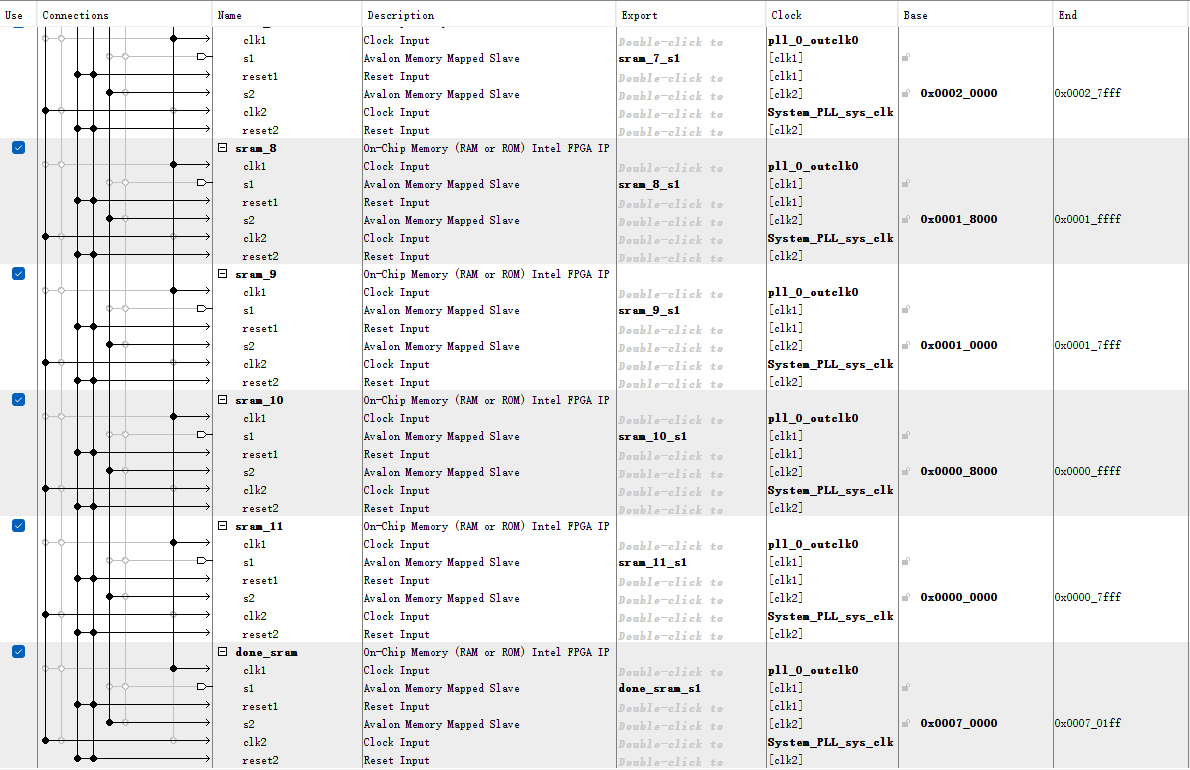
Therefore, we need to segment the SRAM into a total of 12 blocks, with each SRAM block capable of storing 128x128 16-bit data elements. This segmentation increases the number of SRAM ports, allowing up to 12 concurrent memory accesses, which significantly enhances performance.
All of the SRAMs are mounted on the AXI bus, and their addresses are contiguous. This setup simplifies memory access through C programs. Additionally, the SRAM operates at a frequency of 250 MHz. As a result, the processor and functional units can treat the memory as combinational logic memory, greatly simplifying the design. The Qsys design is shown in the figure below.
In addition to the Data SRAM mentioned above, within the Qsys system, there are also "Instruction SRAM" and "Instruction Done SRAM". The "Instruction SRAM" is used to store instructions sent from the ARM CPU. The data width is 128 bits, and depth is 512. The "Instruction Done SRAM" is used to indicate that an instruction has been fully processed and completed. The data width is 8 bits, and depth is 512. This separation of memory functions optimizes the flow and management of both data and instructions within the system.
Qsys design
Qsys design
4.4 Half-precision Floating-point Module
We used IEEE 754 half-precision floating-point format (fp16) for arithmetic operations, utilizing 16 bits: 1 sign bit, 5 exponent bits, and 10 fraction bits, as shown in the figure below. Leveraging fp16 arithmetic rules reduces memory usage and computational overhead, vital in resource-limited settings. Although less precise than fp32, fp16 offers a balance between accuracy and efficiency.
FP16
We refered to some open-source implementations of floating-point module. We reused some code from the reference and implemented hardware modules of half-precision floating-point arithmetic, including addition, multiplication, and comparison operations.
Addition: In half-precision floating-point addition, two numbers are aligned based on their exponents. the number with the smaller exponent is right-shifted to match the exponent of the larger number. and then their fractions are added together. After addition, the result normalized to meet the requirements of IEEE754. Overflow and underflow conditions are considered during this process, with special handling for cases where the result exceeds the representable range.
Multiplication: For multiplication in half-precision floating-point, the exponents of the two numbers are added together. The resulting exponent is judged whether there is an overflow or underflow. Subsequently, the fractions are multiplied and the result is rounded and normalized to fit within the 10 bits of fraction representation.
Comparison: In binary floating-point comparison of two FP16 numbers, the process initiates by assessing the sign bits. A positive number is greater than a negative number. For numbers with identical signs, the exponents are compared next. A larger exponent indicates a larger number. If the exponents match, the comparison proceeds to the mantissas, where the number with the larger mantissa is determined to be larger.
4.5 Convolution Module
The Convolution Verilog module is designed to perform convolution operations. This module functions by interfacing with external SRAM for fetching input data and storing output results. It handles three memory interfaces: one for the input matrix, another for the convolution kernel, and a third for the output matrix. These interfaces manage their respective read and write operations through designated address and data. Control signals such as clock, reset, start manage the operational flow. The size of the input matrix and kernel are specified to allow different convolution size. We basically used the same interface for all the function units, so it is easier to integrate all the function units with the processor.
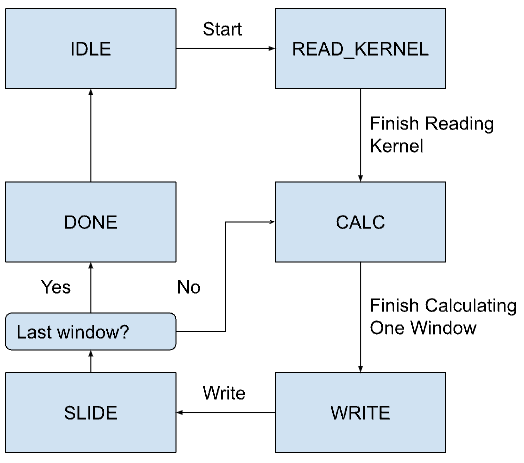
Convolution Module State Machine
Within this module, a state machine controls the convolution process through six states, as shown in the figure above. Initially, in the IDLE state, the module remains in a waiting mode until the start signal is activated. Upon activation, the module transitions to the READ_KERNEL state, where it reads the kernel data from SRAM and stores the kernel data into internal registers. Once the kernel is fully loaded, the module moves to the CALC state.
In the CALC state of the convolution module, convolution computations are carried out by multiplying the data from the input matrix with kernel values and accumulating the results, while also adjusting the addressing within the input matrix to align with kernel dimensions. Depending on the progress, the module may either continue in CALC to process additional matrix segments or transition to WRITE to store results in the SRAM output matrix. If further segments require processing, it shifts to SLIDE to adjust the convolution window's starting point on the input matrix, facilitating continuous operation. The process ends in the DONE state where the module signals completion via the done indicator, resets internal registers, and prepares for a new operational cycle by going back to the IDLE state. This state machine ensures the convolution is efficiently processed, with accurate data handling and systematic storage.
4.6 Relu Module
The ReLU (Rectified Linear Unit) function is commonly used in neural networks to introduce non-linearity, and it sets any negative input value to zero while keeping positive values unchanged.
ReLU Module State Machine
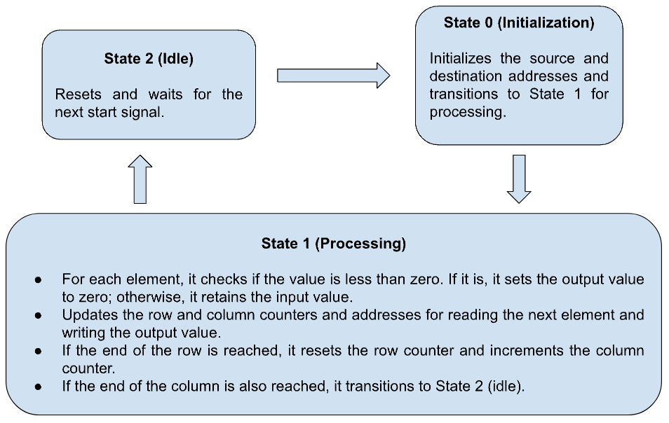
The ReLU activation function present in our functional unit is implemented using a finite state machine approach. The ReLU function is a common non-linear activation function used in neural networks, which sets any negative input value to zero while retaining positive values. The FSM begins in an idle state (State 2), where it waits for a start signal. Once the start signal is received, it transitions to the initialization state (State 0), where it sets the starting addresses for both reading from the input matrix and writing to the output matrix, and resets internal counters for rows and columns to zero. The FSM then moves to the processing state (State 1), where it iterates through each element of the input matrix. For each element, the module reads the data from the input matrix (source), checks if the value is less than zero, and if so, sets the corresponding output value (destination) to zero; otherwise, it keeps the input value. This processed value is then written to the output matrix at the current destination address, and the write enable signal is asserted to facilitate this write operation. The FSM continues this process by updating the addresses and counters to traverse through the entire matrix. It increments the row counter and, when the end of a row is reached, it resets the row counter and increments the column counter. This cycle continues until the entire matrix is processed. Once all elements are processed, the FSM transitions back to the idle state (State 2), where it sets the ‘done’ signal to indicate the completion of the ReLU operation. The FSM remains in this idle state until a new start signal is received, at which point it repeats the process. This systematic approach ensures that every element of the input matrix is evaluated and the ReLU function is applied, thereby producing an output matrix where all negative values are replaced with zeros while positive values remain unchanged.
4.7 Pooling Module
Max-pooling is an operation commonly used in convolutional neural networks to reduce the spatial dimensions (width and height) of the input matrix while retaining the most critical information.
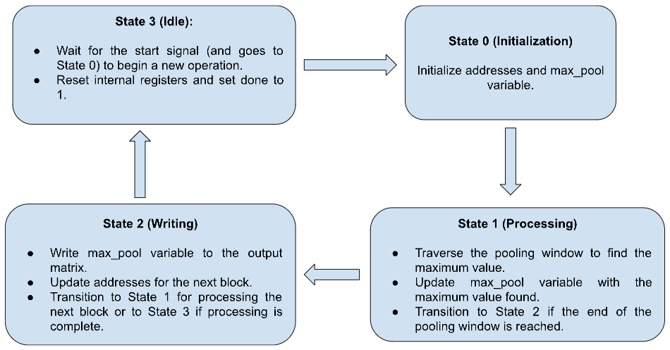
Max Pooling Module State Machine
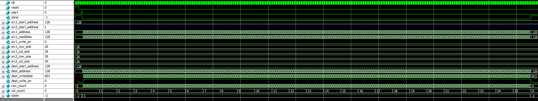
The max-pooling logic used in our functional unit is implemented as a finite state machine that systematically processes blocks of the input matrix to determine the maximum value within each pooling window and writes this value to the corresponding location in the output matrix. The process begins in an idle state (State 3), where the module waits for the ‘start’ signal. Once the ‘start’ signal is received, the FSM transitions to the initialization state (State 0), setting up the initial addresses for reading from the input matrix writing to the output matrix, and resetting the max_pool variable value to zero. The FSM then moves to the processing state (State 1), where it iterates through the elements of the current pooling window. During this iteration, the module updates the max_pool variable whenever a higher value than the current max_pool is encountered. This involves incrementing the row and column counters, adjusting the address for reading the next element, and comparing the read data to the current max_pool. Once the entire pooling window is processed, the FSM transitions to the writing state (State 2). In this state, the module writes the max_pool value to the output matrix, updates the destination address for the next write operation, and resets the row and column counters. If all blocks have been processed, indicated by the counter - ‘val’ variable reaching the total number of pooling windows, the FSM transitions back to the idle state (State 3), signaling that the max-pooling operation is complete by setting the ‘done’ signal to 1. Otherwise, it returns to the processing state (State 1) to continue with the next block. The logic ensures that the module reads from the input matrix, computes the maximum value within the pooling window, and writes this value to the output matrix iteratively until the entire input matrix is processed.
4.8 Matrix multiplication Module
This module used the same interface as convolution module. But Matrix multiplication requires that the number of columns in the first matrix matches the number of rows in the second matrix. Because of this, this module only need three inputs to configure: the number of rows in the first matrix, the number of columns in the first matrix (which should be the same as the number of rows in the second matrix), and the number of columns in the second matrix. These three parameters ensure that the matrices can be multiplied together correctly.
The Verilog module implements a state machine for matrix multiplication, including four main states: IDLE, CALC, WRITE, and DONE. In the IDLE state, the module awaits the activation of the start signal, during which all addresses and counters are initialized, and the done signal is set to 1 to indicate that no computation is currently underway. Upon receiving the start signal, the module transitions to the CALC state, where it begins to perform matrix multiplication incrementally. Here, an internal accumulator sum is used to compute the results. Once the computation of a row is complete, the state machine moves to the WRITE state, writing the results to the destination address. In the WRITE state, address pointers are updated to start processing the next row, setting up for the next computation cycle. If all data has been processed, the state machine enters the DONE state, where all counters and addresses are reset, and the done signal is set to 1, indicating that the computation is complete. The state machine then returns to the IDLE state to wait for the next compute command. The entire process is controlled meticulously through precise state transitions to ensure efficient and accurate execution of matrix multiplication, making it suitable for hardware-level implementation of efficient matrix operations.
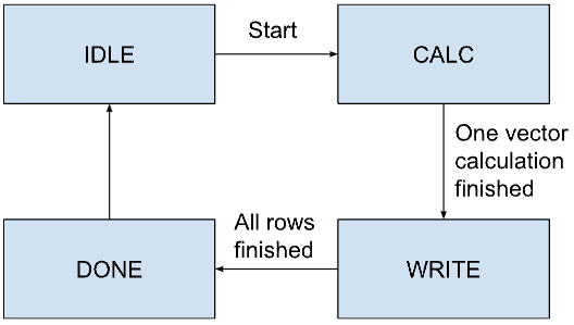
Matrix multiplication Module State Machine
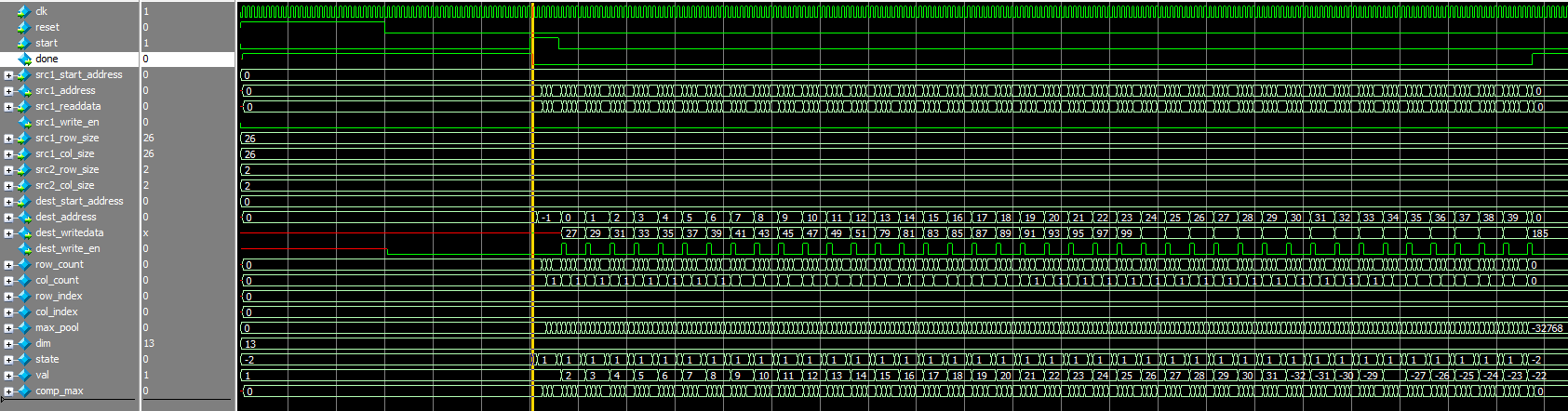
In the context of neural networks, matrix multiplication is fundamental for executing operations in fully connected layers. In our CNN model, where the weight matrix is 507×10 and the input vector, once flattened, is 507×1. When these two are multiplied, the resulting matrix is 10×1. This outcome occurs because each element of the resulting vector is the sum of the products of corresponding elements in the weight matrix and the input vector. Each of these sums represents the total weighted input to a single neuron in the network. This multiplication efficiently combines all inputs with their respective weights, which is precisely the computation needed in a fully connected neural network layer, where every input is connected to every output through these weights. Matrix multiplication serves as an efficient mathematical operation for handling the computations within fully connected layers.
4.9 Matrix Element Arithmetic Modules
Matrix Element Arithmetic Modules include matrix addition, matrix subtraction, and matrix element-wise multiplication. For matrix element arithmetic, the size of the two input matrix should be the same. So these modules can use the same interface and the same state machine. The only difference between these modules is that they use different arithmetic modules when calculating.
Let's take matrix addition as an example to explain the state machine, as shown in the diagram below.
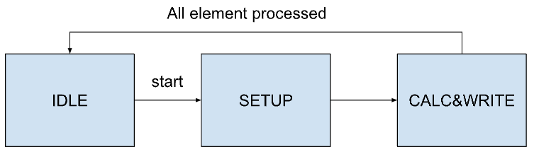
Matrix Addition Module State Machine
Initially, in state IDLE, the module remains idle, waiting for the start signal. Upon receiving this signal, it transitions to state SETUP to initialize the addresses of both source matrices and the destination matrix. This setup prepares the module for the core operation of element-wise addition. Once the setup is complete, the machine enters state CALC&WRITE, the primary state for executing matrix addition. Here, it iteratively processes each element of the matrices, updating the corresponding addresses and counters. The floatAdd sub-module computes the sum of corresponding elements from the source matrices, which is then written to the destination matrix. This state continually checks if all elements of the current row have been processed before moving to the next, ensuring each part of the matrix is accurately handled. The completion of the entire matrix triggers a transition back to state IDLE. In this state, the machine resets all parameters and waits for another start signal, indicating readiness for a new operation.
4.10 Things We Tried
Initially, we tried using fixed-point arithmetic instead of floating-point calculations. However, we found that the precision of fixed-point arithmetic was too low and the numerical range did not meet our requirements. As a result, we ultimately decided to use floating-point operations.
Additionally, we attempted to increase the frequency of the function units. However, since the floating-point module is based on combinational logic, increasing the frequency of the function unit led to timing issues in the critical path, resulting in errors. Through our trials, we managed to achieve a maximum frequency of 25 MHz for the function units.
We also experimented with increasing the frequency of the SRAM. However, the SRAM could not perform write operations normally at 300 MHz. At 250 MHz, the SRAM functioned correctly in all respects.
Lastly, we tried modifying the frequency of the AXI bus. It appears that the AXI does not operate correctly at any frequency exceeding 100 MHz. Therefore, we set the operating frequency of the AXI to 100 MHz.
5. Results
5.1 Testing Results
We first need to test each function unit and the floating point modules. We accomplish this by writing a unit testbench to test all the modules. The results of these tests are as follows.
Here are the test results of FP16 addition and multiplication modules.

FP16 Add Waveform

FP16 multiplication Waveform
Here is the test result of convolution module, the input matrix size is 28*28, kernel size is 3*3.
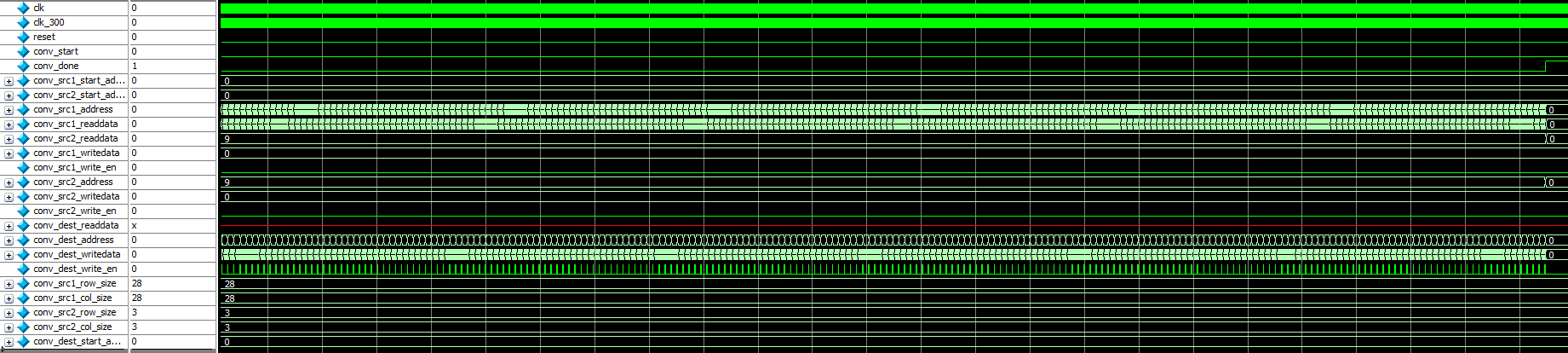
Convolution Waveform
Here is the test result of ReLU module, the input matrix size is 26*26.
ReLU Waveform
Here is the test result of max-pooling module, the input matrix size is 26*26, kernel size is 2*2.
Max-pooling Waveform
Here is the test result of matrix multiplication module, the input matrices are 507*10 and 507*1, output size is 10*1.

Matrix Multiplication (Fully Connected) Waveform
Here is the test result of the processor. It can be seen from the waveform that 3 function units are running in parallel(conv, relu, and dot). This proves that the superscalar out-of-order processor is working correctly.
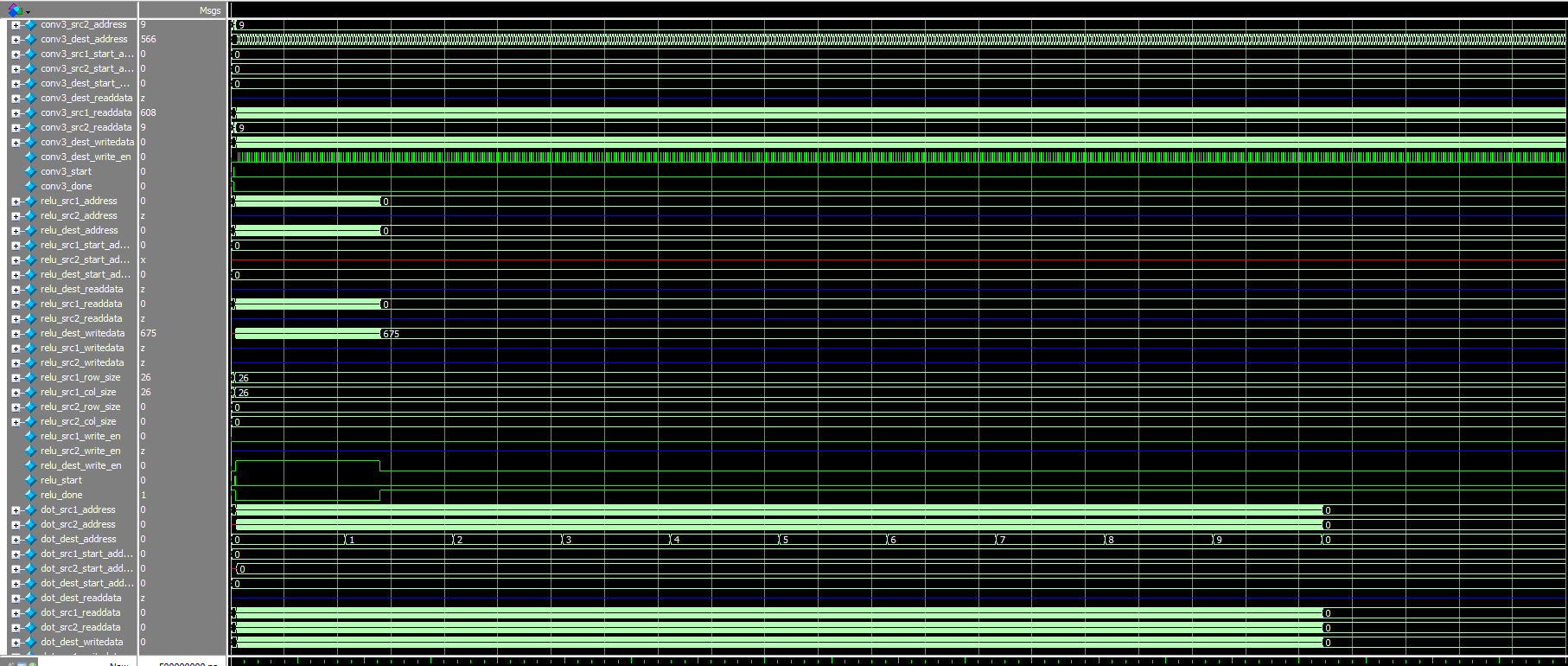
Parallel computation in the Processor
Here is the result of using the NPU for CNN inference. The matrix output above is MNIST image data normalized by PyTorch and read by a C program. It is recognizable as the digit 7. The output below displays the inference result, specifically the output of the fully connected layer. The result shows that the data at the seventh position is the largest, indicating that the inferred result is the number seven.
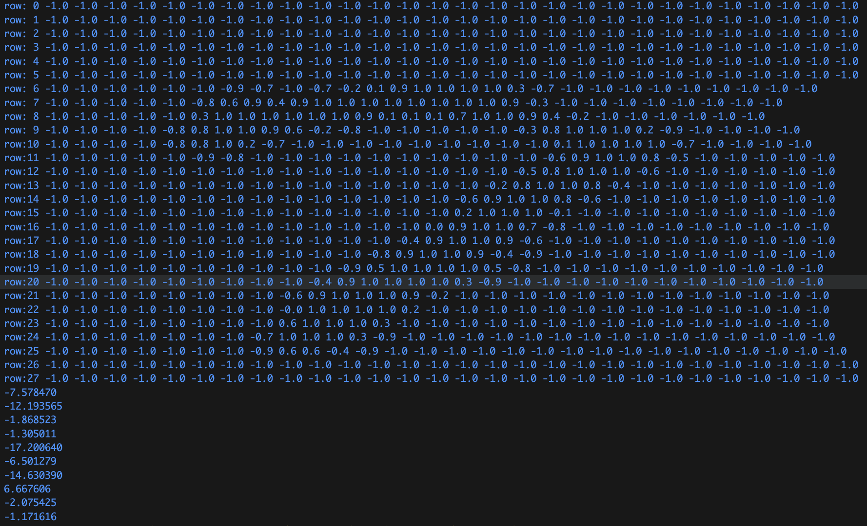
Inference using NPU
5.2 Speed of Execution
We built testbenches and conducted testing using the same network size as the trained neural network. According to the testbench waveform shown above, the computation time is calculated in the following table. In the actual hardware, the clock frequency is 25Mhz.
| Computation | Cycles | time/us | 、
|---|---|---|
| Conv | 7444 | 297.76 |
| ReLU | 678 | 27.12 |
| Pooling | 207 | 8.28 |
| Multiplication | 5080 | 203.2 |
5.3 Accuracy
The trained CNN model has an accuracy of 96.6% after training for 5 epoches.
CNN accuracy
5.4 Usability
The entire system is very user-friendly. It only requires a basic understanding of neural networks. Users can simply call functions within the C program to generate the necessary instructions. There is no need to understand the specific details of the algorithm implementation. By calling these functions to generate the corresponding instructions, the NPU can be utilized to accelerate computations.
6. Conclusions
6.1 Conclusions
The development of this NPU was a good success and met the design expectations. By incorporating dedicated functional units for matrix operations, convolution, and activation functions, the NPU is tailored to efficiently execute CNN models with high computational speed. The architecture's out-of-order processing, combined with a robust memory subsystem and a sophisticated instruction set, ensures optimal performance and flexibility. Despite the initial challenges with floating-point arithmetic, the NPU demonstrates promising results, achieving high accuracy on the MNIST dataset.
6.2 Future Plans
Moving forward, enhancing the functional units, optimizing performance, expanding memory capacity, and improving software support will be crucial steps in further advancing the NPU's capabilities.
In our future plans, we aim to introduce additional functional units to handle more complex operations, such as batch normalization, and various activation functions beyond ReLU. Expanding support for other neural network models such as RNNs, LSTMs, and Transformers to make the NPU more versatile is another future proposal.
By implementing power management techniques to enhance the energy efficiency of the NPU, we can make it suitable for mobile and embedded applications. Making the NPU adapt to edge AI applications, such as real-time image and video processing, autonomous vehicles, and IoT devices will make it a highly useful resource.
Appendix A: Permissions
The group approves this report for inclusion on the course website.
The group approves the video for inclusion on the course youtube channel.
Appendix B: Code
All code and project files can be found on Github: Link.
Appendix C: Contribution

Yuqiang Ge
Netid: yg585
Instrunction Set Design,
Processor Architecture Design,
Memeory System Design,
Function Units Design and Testing,
C Program Design,
Python Program Design

Kapinesh Govindaraju
Netid: kg534
Pooling Module Design,
ReLU Module Design,
Testing Designed Modules
(for functional units)

Sona Susan Jacob
Netid: sj778
Pooling Module Design,
ReLU Module Design,
Testing Designed Modules
(for functional units)