Using a hardware timer.
Each specific NiosII processor has different characteristics, so when talking about an assembler program, you also have to specifiy the specific NiosII that it runs on. I generated a basic economy cpu (E type) with two 8-bit parallel ports and a timer. The configuration is shown below. It is very similar to the DE2 SOPC tutorial version. To write assembler code, you need to notice the i/o addresses for each port and for the timer. Notice also that the timer uses IRQ 1 which means that we need to set bit 1 in control register 3 to enable a timer interrupt. By double-clicking on the memory tab you can check the amount of memory created. This is useful for positioning a stack at the top of memory. In this case I generated 4k of memory.

If you open the More cpu options tab, you can get the memory location that the interrupt unit uses for exception code. In this case it is 0x0000020, which is the default.

The SOPC produces some verilog files which need to be combined with a top-level module and FPGA pin definitions using QuartusII. The top-level module in this case is very simple, but could contain arbitrary circuitry (see #2 below).
// Implements a simple Nios II system for the DE2 board.
// Inputs: SW7-0 are parallel port inputs to the Nios II system
// CLOCK_50 is the system clock
// KEY0 is the active-low system reset
// Outputs: LEDG7-0 are parallel port outputs from the Nios II system
module TimerTest(SW, KEY, CLOCK_50, LEDG);
    input [7:0] SW;
    input [0:0] KEY;
    input CLOCK_50;
    output [7:0] LEDG;
    // Instantiate the Nios II system module generated by the SOPC Builder:
    // nios_system (clk, reset_n, out_port_from_the_LEDs, in_port_to_the_Switches)
    NiosII niosIItimer(CLOCK_50, KEY[0], LEDG, SW);
endmodule
The output of the QuartusII compilation is an .sof file to be downloaded to the DE2 Using QuartusII, and a .ptf file to be used by the NiosII debug client. The ptf file describes the custom cpu to the debugger client. At this point we have built the hardware. Now we need a program to run on it. A simple assembler program transfers the position of 8 switches to 8 LEDs, and once a second inverts the LEDs. The timing is done using the hardware timer module described in the SOPC builder. There are several things to notice in the code:
- The 16-bit timer control registers (described in Timer Core with Avalon Interface) are spaced 32 bits apart in memory address starting at the address given by the SOPC builder table.
- The timer interrupt flag (
TO) has to be cleared manually in the ISR. - There are 3 levels of interrupt control on the NiosII. There is a master interrupt enable (
PIE) in the cpustatusregister (control register 0). There are 32 individual interrupt enable bits for each different interrupt in theienablecontrol register. There is an interrupt enable on the specific hardware, in this case the timerITObit. - Seven NOPs have to be inserted between the reset entry point (
0x00) and the exception entry (0x20). The exception entry is located at0x20in order to put it on the second cache line (if there is a cache). - The exception return register (
r29) must be decremented by 4 before issuing the return-from-exception (eret), only if the exception is an interrupt (but not if it a software trap). See the NiosII Processor Reference Handbook. - Branches and jumps do not have a branch delay slot. See the NiosII Processor Reference Handbook.
- A stack and
pushandpopmacros were defined to make interrupt handling more general. You must set up the stack if you usepushorpop. An general interrupt handler should check for multiple interrupt sources and prioritize them.
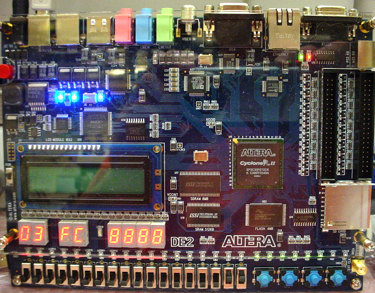
Using the same NiosII processor and the same assembly program as in #1, the top-level verilog module was changed to support 7-segment readout of the switch values and the blinking green LEDs. The switch setting are displayed on the left-most two digits, while the green LED value is displayed on HEX5:4 One short module was added along with the circuitry to drive the four 7-segment digits. An image below shows the right-most two switches in the up position. A short mpeg shows the blink rate.
Modifying the top-level hardware again to include a bit toggling on the parallel i/o connector allows us to measure the timer frequency on an oscilloscope. Setting the hardware timer period to
0x00010000 should produce a frequency of clk/period/2 or 5e6/2^16/2=381.5 Hz. The division by 2 is because two periods is equal to one cycle when the output is toggled on each period. My scope shows 381.4 Hz, which is within the accuracy of the scope itself. Setting the period to 0x00000100 should produce 97. 66 kHz and actually produces 98.0 kHz, as close as I can read. However there is about 0.6 microseconds of jitter in the period. Reducing the period to the minimum which will work, 0x00000070, suggests that the interrupt service routine (plus entry overhead) takes about 110 cycles to complete. If you open the SOPC with this design, you will find that I used the low-performance NiosII cpu (e version), which is multicycle. The image below shows the trace with a period of 0x00000100. 
The cpu was changed to the S (pipelined version) with instruction cache, but runs the same code as above. Now the timing jitter is about 0.1 microseconds, but varies from 0.0 to 0.18 microseconds. A timer period of
0x0030 gives a frequency of 515 kHz against the calculated 521 kHz. The timer is accurate to at least 4 places (the limit of my scope) at lower frequencies. The minimum relable timer period is about 32 cpu cycles. The timer ISR has 10 instructions (movia, push, and pop are two-instruction macros). It probably takes two or three cycles to get in and out of the ISR (storing ea, status, etc), so I am guessing about 2 cycles/instruction. This is consistent with Altera performance numbers. 

.sof file to be downloaded to the DE2 Using QuartusII, and a .ptf file to be loaded into the Debug Client.