Hardware Details
The direction that we took with this project emphasized careful hardware selection and design. Because of the concept of our project, a portable wireless thermometer, it was always understood that the final product would have to be completely mobile. This meant that we needed protoboards and batteries. The STK500, breadboards and power supplies were good starting points, but are not used in the final design. Our plan was to lay out the major components on breadboards and use the STK500 as a support board (we used two STK500s in the beginning) because we were very familiar with the STK500 and breadboard technology that it minimized debugging time. We flashed the Mega32s with the transmitter and receiver circuits on the breadboards. Using Meghan’s software we were able to debug these circuits with a small LCD. In the picture below the LCD is on the right hand side of the picture on its own breadboard. The transmitter and receiver were both placed on the same breadboard yet weren’t connected electrically in any way (see Figure 20). The STK500 on the left has the Mega32 that operated as the transmitter and the STK500 on the right has the Mega32 that acts as the receiver.
Meanwhile, we soldered all the standard parts to the protoboards. These included: Atmel Mega32 in a 40-pin dip mount, 10 capacitors (22pF, .1µF, 1µF), 3 resistors (100Ω, 330Ω, 100kΩ), PGM pins, 16MHz crystal, LED, jumper pins, power hookup and the power regulator. We flashed the protoboards to make sure that all the connections were right. We were looking at using the Mega16 or the Tiny45 on the protoboards instead of the Mega32 because we could get them for much cheaper, but we settled on the Mega32 because the Mega16 does not have enough space in memory for speech and the Tiny45 does not have a UART so it would have been much more difficult to implement wireless communication.
When we were satisfied with the transmitting and receiving we transferred the transmitter circuit to the protoboard. There were also a couple errors in Meghan’s code, and he helped us to work those out. Afterward we started with putting the transmitter on the protoboard. We transferred one major part of the system at a time so that we could debug the transmitter while remaining confident in the reliability of the receiver. As it turns out such a precaution was not necessary because the transmitter transferred to the protoboard and did not require any debugging - it worked immediately after flashing for the first time. The transmitter really was not touched after that point the only further adjustments that we made to our original transmitter unit was to add a 9V battery clip and a Wheatstone bridge, which allowed for the unit to interface with the thermistor. See Figure 21 for a schematic of the transmitter unit.
The finished product for the transmitter can be seen in the Figure 22. In the transmitter, receiver and audio amplifier the wire color scheme is typically the same. Red wire is for Vcc, or 5V, black is for ground and yellow or blue is for wire that carries a data signal. Other colors are for wires that fulfill a support function that are not power, ground or information bearing. An example is the gray wire, which in the below picture is used for the antenna and the DC choke.
After finding that the transmitter worked on the protoboard we started putting the components required to make a functional receiver unit on the other protoboard. The receiver board proved to be much more sophisticated and much harder to debug. Since we had the standard elements on the board (Mega32, resistors, etc.), the receiver, the attachment for the LCD, and the pushbuttons - the board was extremely crammed and space for attachments became difficult to procure. Looking back it would have been useful to have a plan of how we were going to layout the different components of the circuit, but since a great deal of the designing and layout happened as the boards were getting soldered a well thought out plan would have been modified anyway. We knew what we wanted to implement and how to implement it, but didn’t really consider where each component would physically go on the board.
Figure 23 is a higher level circuit schematic for the receiver unit. Figures 24, 25, and 26 that show the BJT inverter used in both the receiver and transmitter, and the pushbutton layout and the power amplifier on the receiver unit.
The lack of abundant space with which to mount parts on the receiver’s board contributed to using more creative methods of soldering, such as connecting soldering points by metal wire by using solder as an adhesive or soldering components on the underside of the board as well as on the top. As can be seen Figure 27, the majority of the wiring and components are on the top of the board whereas the connections for the LCD, extra wiring and some resistors are on the bottom. Again red wires are for Vcc, black for ground, and yellow and blue for information.
The third smaller and microcontroller deficient protoboard that we used was used for the audio amplifier. Since we need a speaker for the speech it would have been impossible to mount one as together with an amplifier on the crowded receiver board. We started trying to implement the speaker by directly connecting it to PB3 of the Mega32 but quickly found that that did not work with either a piezo or traditional 8Ω speaker. We then moved on to putting the speaker signal through a low pass filter and could very faintly hear the speech output by the Mega32. We decided on using an amplifier because the amplitude of the power needed to be greatly increased to make the sound audible. We tested out a few configurations with operational amplifiers to take advantage of the gain those circuits grant but found them to be too noisy or inconsistent. So, we started looking into using an audio amplifier that was all in an IC so that it would save us the trouble of making and debugging one. After combing the lab for one we finally found a single LM386 in one of the IC drawers that had a large variety of random ICs (see Figure 28). This IC proved to be very useful because after using the amplifier schematic on page 5 of the data sheet we had speech coming out of our 8Ω speaker. A little more tweaking and we had fairly clean speech. We then transferred the practice circuit from the breadboard to a protoboard that we found in one of the scrap boxes in the lab.
Figures 29 and 30 show our practice circuit and the more compact speech protoboard. The picture of the practice board is included because it shows a good layout of the audio amplifier so that future groups may use our design.
Once everything was on the protoboards, some tweaking had to be made so that the system would perform how we wanted it to. For example, a capacitor had to be added to the audio amplifier board to cut off the direct connection between the 9V battery and the speaker.
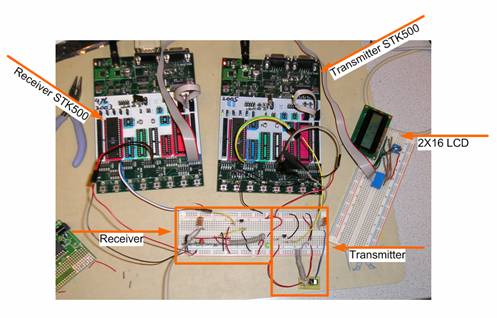
Figure 20: Breadboard setup of receiver and transmitter circuits
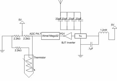
Figure 21: Transmitter unit schematic
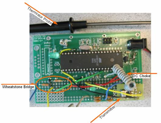
Figure 22: Finished receiver unit
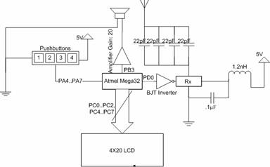
Figure 23: Receiver unit circuit schematic
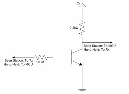
Figure 24: Inverter schematic
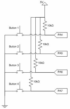
Figure 25: Pushbutton schematic
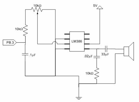
Figure 26: Audio amplifier schematic
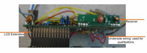
Figure 27: Detail on physical receiver unit design
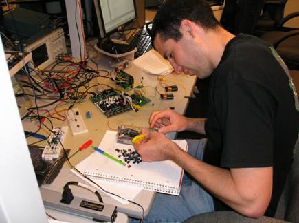
Figure 28: Jeff searching through a drawer of ICs for our LM386

Figure 29: Audio amplifier circuit on breadboard
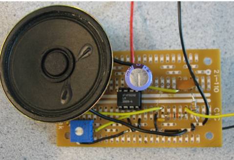
Figure 30: Compact audio amplifier circuit on a protoboard.
|